Note: Descriptions are shown in the official language in which they were submitted.
:~, 2006857
-1 -
PHOTOSENSITIVE MEMBER FOR ELECTROPHOTOGRAPHY
FIELD OF THE INVENTION AND RELATED ART
The present invention relates to a
5 photosensitive member for electrophotography,
particularly to a photosensitive member for
electrophotography comprising a low-molecular weight
organic photoconductor capable of providing improved
electrophotographic characteristics.
Hitherto, there have been proposed a large
number of organic photoconductive polymers to be used
for electrophotographic photosensitive members, such as
polyvinyl carbazole. These conventional organic
polymers are superior to inorganic photoconductive
materials in lightness (in weight), film-forming
property, etc., but are inferior to the latter in
sensitivity, durability, stability to environmental
change, mechanical strength, etc.
On the other hand, there have been proposed
several low-molecular weight organic photoconductive
materials such as hydrazone compound (U.S. Patent
4,150,987), triaryl pyrazoline compound (U.S. Patent
3,837,851), and 9-styryl anthracene (Japanese Laid-Open
Patent Application (JP-A, KOKAI) Nos. 94828/1976 and
94829/1976)
In a case where the conventional low-molecular
weight organic photoconductors represented by those as
2006857
--2--
described above are used, the above-mentioned defect in
film-forming property, which has conventionally posed a
problem in the field of the organic photoconductive
polymer, may be obviated by appropriately selecting a
binder to be used in combination therewith. However,
these conventional organic photoconductors have not
provide a sufficient sensitivity.
In such a viewpoint, there has recently been
proposed a laminate-type structure wherein the
photosensitive layer is function-separated into a
charge generation layer and a charge transport layer.
The electrophotographic photosensitive member
comprising such a photosensitive layer may be improved
in sensitivity to visible light, charge retentivity,
surface strength, etc.
As the charge-transporting substance
constituting the above-mentioned transport layer, a
large number of organic compounds have heretofore been
proposed. Examples thereof include: pyrazoline
compounds (Japanese Laid-Open Patent Application No.
72231/1977), hydrazone compounds (U.S. Patent 842,431
and Japanese Laid-Open Patent Application No.
52063/1980), triphenylamine compounds (Japanese Laid-
Open Patent Application Nos. 195254/1982 and
58445/1979), stilbene compounds (Japanese Laid-Open
Patent Application Nos. 151955/1979 and 198043/1983),
carbazole compounds (Japanese Laid-Open Patent
2006857
Application Nos. 150128/1979 and 58451/1988),
benzothiophene compounds (Japanese Laid-Open Patent
Application No. 110835/1979), etc.
However, in the electrophotographic
5 photosensitive member using the conventional low-
molecular weight organic compound as the charge-
transporting substance, the sensitivity and other
electrophotographic characteristics are not necessarily
sufficient, and the light part potential and dark part
10 potential are liable to show a considerable change,
when charging and exposure operations are conducted
repetitively.
Accordingly, with respect to such an
electrophotographic photosensitive member, there is
15 still room for improvement.
SUMMARY OF THE lr~v~;NlION
An object of the present invention is to
provide an electrophotographic photosensitive memh-~r
20 which has solved the above-mentioned various problems
encountered in the conventional photosensitive member.
Another object of the present invention is to
provide an electrophotographic photosensitive member
using a novel organic photoconductor which may easily
25 be produced, is relatively inexpensive and is excellent
in durability.
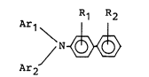
According to the present invention, there is
_4_ 2006857
provided a photosensitive member for electrophoto-
graphy, comprising an electroconductive substrate and a
photosensitive layer disposed thereon, wherein the
photosensitive layer comprises a triarylamine compound
represented by the following general formula (I):
Ar1 R1 R2
/ N ~ (I),
Ar2
wherein Ar1 and Ar2 respectively denote a benzene ring
capable of having a substituent; at least one of Ar1
and Ar2 has an electron-donating substituent; and R1
and R2 respectively denote a hydrogen atom, alkyl or
alkoxyl.
These and other objects, features and
advantages of the present invention will become more
apparent upon a consideration of the following
description of the preferred embodiments of the present
invention taken in conjunction with the accompanying
drawings.
BRIEF DESCRIPTION OF THE DRAWINGS
Figures 1 and 2 show infrared absorption
spectra of Compound Example Nos. 10 and 13,
respectively, according to the KBr tablet (or pellet)
method.
~2
200~857
- -5-
DETAILED DESCRIPTION OF THE INVENTION
In the above general formula (I), Ar1 and Ar2
respectively denote a benzene ring capable of having
one or more substituent. At least one of Ar1 and Ar2
has an electron-donating (or electron donative) group
as a substituent. The "electron-donating substituent"
used herein refers to a substituent having a greater
electron-donating ability than a hydrogen atom.
Specific examples of the electron-donating
group may include: alkyl groups (preferably C1 to C3)
such as methyl, ethyl and propyl; alkoxyl groups
(preferably C1 to C3) such as methoxy and ethoxy
groups; substituted amino group (preferably, di-
substituted amino group) such as dimethylamino and
diethylamino groups; etc. The substituent of the amino
group may preferably be C1 to C3.
R1 and R2 respectively denote a hydrogen atom,
alkyl groups (preferably C1 to C3) such as methyl,
ethyl and propyl; alkoxyl groups (preferably C1 to C3)
such as methoxy and ethoxy.
Incidentally, it has heretofore been known
that a triarylamine compound is used as a charge-
transporting substance. However, in general, such a
conventional triarylamine compound has provided a low
sensitivity.
In the present invention, an electron-donating
substituent is introduced into at least one of the
2~ 8S~7~
-6-
benzene rings of Ar1 and Ar2 in the above-mentioned
formula (I). As a result, according to the present
invention, there is provided a charge-transporting
substance which is capable of providing high
sensitivity and high durability, and may easily be
synthesized inexpensively, whereby the problems
encountered in the prior art have been solved.
Particularly, a compound of the above-
mentioned formula (I) having an oxidation potential of
0.9 V or below wherein at least one electron-donating
group is introduced into the benzene ring of Ar1 and/or
Ar2 may provide an excellent electrophotographic
characteristic. Further, such a compound having an
oxidation potential of 0.60 V or above and 0.88 V or
below may provide an electrophotographic photosensitive
member having an extremely high sensitivity.
According to our investigation, it may be
considered that the compound having an oxidation
potential of above 0.9 V only provides insufficient
carrier injection property from a charge-generation
layer. On the other hand, the compound having an
oxidation potential of below 0.60 V provides relatively
large dark decay and relatively high residual
potential to deteriorate the electrophotographic
characteristic, while the reason for such a phenomenon
is not necessarily clear.
Therefore, among the compounds represented by
2006857
_ -7-
the above-mentioned general formula (I), a compound
having an oxidation potential of 0.6 - 0.88 V wherein
at least one of the benzene rings of Ar1 and Ar2 has an
electron-donating substituent is particularly preferred
since such a compound may provide an electrophoto-
graphic photosensitive member having excellent
electrophotographic characteristics.
Representative examples of the compound of the
above-mentioned formula (I) are described hereinbelow.
However, the compound represented by the formula (I)
usable in the present invention is not restricted to
these specific examples.
In the following description, ''Eoxll denotes an
oxidation potential (volt).
~ -8-
2006857
<Compound Examples>
1. CH
N ~
(Eox = 0.87)
2. CH3
N ~
(Eox = 0.88)
3- C2H5
N ~
(Eox = 0.86)
15 4. C3H
N ~
(Eox = 0.86)
5. CH30
~ N ~
(Eox = 0.81)
6. C2H5O
~ N ~
(Eox = 0.86)
B
-- -9- ~)068~;7
7. CH3
CH ~ N ~
~ (EoX = 0.87)
8. CH3
CH3
N ~
(EoX = 0.85)
9. CH3
CH30
~ N ~
(EoX = 0.78)
10. CH3
~ N ~
CH3 ~ (EoX = 0.86)
20 11. CH3
- N ~
CH3 ~ (EoX = 0.86)
Z006857
-- -1 O-
12. CH3
~,,
~ N ~
CH3 (EoX = 0.88)
13. CH30
N ~
CH30 ~ (EoX = 0.69)
14. CH3
N
,_ / ~
CH3 ~ ~ CH3 (EoX = 0.85)
15. C2H5
N ~
C2H5 ~ (EoX = 0.84)
16. CH3 ~ CH3
N ~
CH3 ~ CH3 (EoX = 0.83)
17. CH30
N ~
CH3 ~ (EoX = 0-77)
18. C2H5O
N ~
CH30 ~ (EoX = 0.68)
5 19. CH3
~,,
N ~
CH30 ~ (EoX = 0-79)
10 20. CH3
CH3 (EoX = 0.98)
21. ` CH3
CH3
~ N
CH3 ~
- CH3 (EoX = 0.82)
22. CH3 ~
~ ~ CH3
CH3 ~ (EoX = 0.83)
-
2006857
-12-
23. C2H5O
N ~
C2H5O ~ (EoX = 0.68)
524. C3H70
N ~
(EoX = 0.80)
25. (CH3)2CH
\ N ~
(CH3)2CH ~ (EoX = 0.87)
26. C4Hg
/N ~
C4Hg ~ (EoX = 0.85)
27. CH3
N ~
20 - CH3 ~ OCH3 (EoX = 0.82)
28. CH3
CH~
~ N ~
CH3 (EoX = 0-99)
2006857
-- - 1 3 -
29.~OCH3
CH30-
~ N~
CH30~
CH3 (EoX = 0.61 )
30 . ( C2H5 ) 2N~
N~
(EoX = 0.41 )
Measurement of oxidation potential
The oxidation potential values referred to inthe present invention are based on a measurement using
a potential-sweeping method wherein a saturated calomel
electrode was used as the reference electrode, and a
0.1 N solution of (n-Bu)4N+ClO4~ in acetonitrile was
used as the electrolytic solution. In this
measurement, the potential of the working electrode
20 comprising platinum was swept to obtain a current-
potential curve. The oxidation potential was defined
as the potential value corresponding to the peak of the
thus obtained current-potential curve.
More specifically, a sample was dissolved, at
25 a concentration of about 5 - 10 mmol %, in an
electrolytic solution of 0.1 N (n-Bu)4N+ClO4~ in
acetonitrile. Then, a voltage was externally applied
?006857
_ -14-
to the resultant sample solution, and a change in
current was measured while linearly changing the
voltage from a low potential value, thereby to obtain a
current-potential curve. In this measurement, a
counter electrode comprising platinum was used, and the
potential (difference) between the working electrode
and the counter electrode was measured while the
potential (difference) between the reference electrode
and the counter electrode was defined as 0 (zero). In
the present invention, the oxidation potential was
determined by the potential value corresponding to the
peak of the current value in the above-mentioned
current-potential curve.
The above-mentioend Compound Example may be
synthesized in the following manner.
<Synthesis of Compound Example No. 10>
5.0 g (0.025 mol) of ditolylamine, 14.2 g
(0.051 mol) of iodobiphenyl, 13.8 g (0.100 mol) of
anhydrous potassium carbonate, 3.0 g of copper power
(0.047 mol) and 50 ml of ortho-dichlorobenzene were
charged in a three-necked 200 ml-flask equipped with a
thermometer and a condenser, and were heated under
stirring for 20 hours at a reflux temperature. After
the reaction mixture was cooled, the solid content was
removed from the reaction mixture by filtration, the
filtrate was concentrated under reduced pressure, and
then ethanol was added to the resultant product to
20068S~
~ -15-
obtain tan crystals of crude ditolylbiphenylamine.
The crude product was charged to a silica gel
column and was developed by using a toluene-hexane
solvent to obtain 6.8 g (yield = 77.9 %) of white
crystals of purified ditolylbiphenylamine showing a
melting point of 126.5 - 127.7 C. Figure 1 shows an
infrared absorption spectrum chart obtained by
measuring the thus obtained compound by a KBr tablet
(or pellet) method.
10 Elemental analysis (C26H23N)
C(%) H(%) N(%)
Theoretical value 89.36 6.63 4.01
Observed value 89.40 6.61 3.99
Further, the above-mentioned Compound Example
No. 13 was synthesized in a similar manner as described
above. Figure 2 shows an infrared absorption spectrum
chart obtained by measuring the thus obtained compound
in the same r~nner as described above.
Since the compound according to the present
invention may easily be synthesized in a high yield by
using a one-step process as described above, it may
provide an inexpensive electrophotographic
photosensitive member.
The other compounds according to the present
invention may be synthesized in a similar manner as
described in the above Synthesis Example.
In a preferred embodiment of the present
2006857
- -16-
invention, the photosensitive layer is function-
separated into a charge generation layer and a charge
transport layer, and the charge transport layer
comprises the triarylamine compound represented by the
above-mentioned general formula (I) as a charge-
transporting substance.
The charge transport layer according to the
present invention may preferably be formed by
dissolving the above-mentioned compound of the formula
(1) in an appropriate solvent together with a binder,
applying the resultant coating liquid such as solution
onto a predetermined surface, and drying the resultant
coating.
Examples of the binder to be used in the
charge transport layer may include: polyarylate
resins, polysulfone resins, polyamide resins, acrylic
resins, acrylonitrile resins, methacrylic resins, vinyl
chloride resins, vinyl acetate resins, phenol resins,
epoxy resins, polyester resins, alkyd resins,
pol-ycarbonate, polyurethane, or copolymer resins
containing two or more of the recurring units of these
resins, such as styrene-butadiene copolymers, styrene-
acrylonitrile copolymers, styrene-maleic acid
copolymers, etc. Also, other than such insulating
polymers, organic photoconductive polymers such as
polyvinylcarbazole, polyvinylanthracene and
polyvinylpyrene may be used.
20068
~ -17-
In the charge transport layer, the charge-
transporting substance may preferably be used in an
amount of 10 - 500 wt. parts, more preferably 50 - 200
wt. parts, per 100 wt. parts of the binder.
The charge transport layer is electrically
connected to the charge generation layer as described
hereinafter, and has a function of receiving charge
carriers injected from the charge generation layer in
the presence of an electric field and of transporting
these charge carriers to the surface of the charge
transport layer. In such an embodiment, the charge
transport layer may be disposed on the charge
generation layer, or may be disposed under the charge
generation layer. The charge transport layer may
preferably be disposed on the charge generation layer.
It is not preferred that the charge transport layer has
too large a thickness, since there is a certain limit
to the thickness thereof suitable for the transport of
the charge carriers. In general, the charge transport
layer may preferably have a thickness of 5 - 40
microns, more preferably 10 - 30 microns.
The organic solvent to be used in the above-
mentioned formation of the charge transport layer may
vary depending on the kind of the binder used therefor,
and may preferably be selected from those which do not
substantially dissolve the-charge generation layer or a
primer (or undercoat) layer as described hereinafter.
20~8S~
~ -18-
Specific examples of such an organic solvent
may include: alcohols such as methanol, ethanol, and
isopropanol; ketones such as acetone, methyl ethyl
ketone, and cyclohexanone; amides such as N,N-
dimethylformamide and N,N-dimethylacetamide; sulfoxides
such as dimethyl sulfoxide; ethers such as
tetrahydrofuran, dioxane, and ethylene glycol
monomethyl ether; esters such as methyl acetate and
ethyl acetate; aliphatic halogenated hydrocarbons such
as chloroform, methylene chloride, dichloroethylene,
carbon tetrachloride, and trichloroethylene; aromatic
compounds such as benzene, toluene, xylene,
monochlorobenzene, and dichlorobenzene; etc.
The coating may be effected by various coating
methods such as dip coating, spray coating, wire bar
coating, and blade coating. The drying should
preferably be conducted in the sequence of drying at
room temperature to a "tack-free" state and then heat
drying. In general, the heat drying may preferably be
conducted for a time in the range of 5 minutes to 2
hours at a temperature of 30 C to 200 C under
quiescent condition or under blowing.
The charge transport layer according to the
present invention can further contain an additive
selected from various species thereof. Examples of
such an additive may include: plasticizers such as
diphenyl, m-terphenyl and dibutyl phthalates; surface-
-- -1 9-
lubricating agents such as silicone oil, graft-type
silicone polymers, and various fluorocarbons; potential
stabilizing agents such as dicyanovinyl compounds and
carbazole derivatives; anti-oxidizing agents such as
~-carotene, Ni complexes, and 1,4-diazabicyclo[2,2,2]-
octane; etc.
The charge generation layer may comprise a
charge-generating substance. Specific examples of the
charge-generating substance may include: inorganic
charge-generating substances such as selenium,
selenium-tellurium, and amorphous silicon; and organic
charge-generating substances including: cationic dyes
such as pyrylium dye, thiapyrylium dye, azulenium dye,
thiacyanine dye, and quinocyanine dye; polycyclic
quinone pigments such as squarium salt dye,
phthalocyanine pigment, anthanthrone pigment,
dibenzpyrene-quinone pigment, and pyranthrone pigment;
indigo pigment; quinacridone pigment; azo pigment; etc.
These charge-generating substances may be used singly
or as a combination of two or more species. The charge
generation layer may be formed by using such a charge-
generating substance in the form of a vapor deposition
layer or coating layer.
Among the above-mentioned charge-generating
substances, the azo pigment particularly includes
various types. Representative structures of the azo
pigment preferably used in the present invention are
:- - Z006857
-20-
described hereinbelow. When the azo pigment is
represented by a general formula including the
following central skeleton A:
A~N=N-Cp)n
wherein Cp denotes a coupler portion (or coupler
moiety) and n is 2 or 3, specific examples of the
central skeleton A include those comprising the
following structures:
57
-21-
A-1
R R.
~ (R: H, Cl, OCH3)
A-2
~ CH=C ~ (R: H, CN)
A-3
R R
1=CH ~ CH=C ~ (R: H, CN)
R ~-N R
~`X~ (X: O, S R: H, CH3, Cl)
A--5 R
~X~ (X: o, s R: H, CH3, Cl)
- R
A-6 R' R
~ (R: H, CH3, Cl,
R R': H, CH3, ~ )
- 2006857
--22--
A-7
~CH~
A-8
~N~N~ ( X: O, S )
A-9
~ ~CH=CH~ (X: O, S)
A
N--N
~CH=CH-~ H CH ~ (X: O, S)
A- 1 1
~ ~CII=CH~ ( R: H, CH3 )
A
~ (X: CH2, O, S, S02)
A--1 3
O
2006857
--23--
A- 1 4
~ (X:O,S)
A--1 5
N
~¢oY~
A- 1 6
N-N N-N
~X~xJl~ (X: 0, S)
A--1 7
C2H5
A- 1 8
~CH =N-N=CH~
A--1 9
~N~
200~7
-24-
A-20
~ N
A-21
R
~ ~ ~ (R: H, CH3)
A-22
Q~
Specific examples of the coupler portion Cp
include those having the following structures:
Cp-1
HO ~ CONH ~
R (R: H, halogen atom,
alkoxy, alkyl, nitro
group, etc.
n = 1 or 2)
Cp-2
HO ~ CONHR
_ ~ (R: CH3~ C2H5~ C3 7)
<~
H ~ CONHN=CH-R (R: alkyl or ~
O ~ R' = H, halogen atom,
/~\ alkoxy, alkyl, nitro
\~/ group, etc.)
-` 2~S7
-
-25-
Cp-4
H~
(R: H, halogen atom, alkoxyl,
~-~ alkyl, nitro group, etc.)
HIN-
CO
~ N-R or ~ N-R
(R: alkyl, aryl, etc.)
H ~ H ~ n
N ~ O
Cp-7
HO ~ CONH
~0~
N ~
(R1, R2: H, halogen atom,
,/ alkoxy, alkyl,
~ nitro group, etc.
R2 n = 1 or 2)
2006857
-26-
The above-mentioned central structures A and
coupler Cp may appropriately be combined to form a
pigment as a charge-generating substance.
The charge generation layer may be formed by
vapor-depositing such a charge-generating substance by
means of a vacuum vapor deposition device, or by
applying a dispersion containing such a charge-
generating substance dispersed therein, together with
an appropriate binder as desired.
The binder to be used for forming the charge
generation layer may be selected from a wide variety of
insulating resins or alternatively from organic
photoconductive polymers such as polyvinylcarbazole,
polyvinylanthracene, and polyvinylpyrene. There may
preferably be used the insulating resin such as
polyvinyl butyral, polyarylates (e.g., polycondensation
product between bisphenol A and phthalic acid),
polycarbonate, polyester, phenoxy resin, acrylic resin,
polyacrylamide resin, polyamide, polyvinyl pyridine,
cellulose resin, urethane resin, epoxy resin, casein,
polyvinyl alcohol, and polyvinyl pyrrolidone.
The resin may preferably be contained in the
charge generation layer in an amount of 5 - 80 wt. %,
more preferably 10 - 40 wt. ~.
Specific examples of the organic solvent
usable in the coating of the charge generation layer
may include: alcohols such as methanol, ethanol, and
200685~
27-
isopropanol; ketones such as acetone, methyl ethyl
ketone, and cyclohexanone; amides such as N,N-
dimethylformamide and N,N-dimethylacetamide; sulfoxides
such as dimethyl sulfoxide; ethers such as
tetrahydrofuran, dioxane, and ethylene glycol
monomethyl ether; esters such as methyl acetate and
ethyl acetate; aliphatic halogenated hydrocarbons such
as chloroform, methylene chloride, dichloroethylene,
carbon tetrachloride, and trichloroethylene; aromatic
compounds such as benzene, toluene, xylene,
monochlorobenzene, and dichlorobenzene; etc.
The charge generation layer may preferably
contain the above-mentioned charge-generation substance
in an amount as large as possible, so that it may
provide a sufficient absorbance. Further, the charge
generation layer may preferably be a thin layer having
a thickness of 5 microns or below, more preferably 0.01
- 1 micron so that it may inject charge carriers
generated therein into the charge transport layer
within the lifetime of the charge carriers. This may
be attributable to facts such that most of the incident
light quantity may preferably be absorbed into the
charge generation layer to generate a large number of
charge carriers, and that the thus generated charge
carriers may preferably be injected into the charge
transport layer without deactivation due to
recombination or trapping thereof.
-28-
The above-mentioned photosensitive layer
having a laminate structure comprising a charge
generation layer and a charge transport layer may be
disposed on an electroconductive substrate.
The electroconductive substrate may be a
substrate which per se has an electroconductivity such
as those of aluminum, aluminum alloy, copper, zinc, and
stainless steel; alternatively, the above-mentioned
metal substrate or a substrate of a plastic coated
with, e.g., a vacuum vapor-deposited layer of aluminum,
aluminum alloy, indium oxide, tin oxide or indium
oxide-tin oxide alloy, or a mixture of an
electroconductive powder ~such as aluminum powder,
titanium oxide, tin oxide, zinc oxide, carbon black and
silver particles) and an appropriate binder; a
substrate of paper or plastic impregnated with
electroconductive particles, or a plastic substrate
coated with an electroconductive polymer layer. The
electroconductive substrate may be in any form such as
sheet, drum, etc.
Between the electroconductive substrate and
the photosensitive layer, there can be formed a primer
or undercoat layer having a barrier function and an
adhesive function. The primer layer may comprise e.g.,
casein, polyvinyl alcohol, nitrocellulose, ethylene-
acrylic acid copolymer, polyamide (e.g., nylon 6, nylon
66, nylon 610, copolymer nylon, alkoxymethylated nylon,
- Z006857
etc.), polyurethane, gelatin, or aluminum oxide. The
thickness of the primer layer should preferably be 0.1
- 5 microns, particularly 0.5 to 3 microns.
In the electrophotographic photosensitive
5 member according to the present invention, a protective
layer can further be disposed on the photosensitive
layer. Such a protective layer may comprise a resin,
or a resin and an electroconductive material dispersed
therein.
In another embodiment of the present
invention, a pigment or dye having a photoconductivity
may be used as a sensitizer. Examples of such a dye or
pigment include: the above-mentioned disazo pigment,
pyrylium dye, thiapyrylium dye, selenapyrylium dye,
benzopyrylium dye, benzothiapyrylium dye,
naphthopyrylium dye, and naphthothiapyrylium dye, as
described in U.S. Patent 3,554,745; 3,567,438; and
3,586,500.
In a still another embodiment of the present
invention, an euteclic (crystal) complex comprising a
pyrylium dye (as disclosed in U.S. Patent 3,684,502)
and an electrically insulating polymer comprising an
alkylidene-diarylene portion may be used as a
sensitizer. Such an eutectic complex may be formed by
dissolving 4-[4-bis(2-chloroethyl)aminophenyl]-2,6-
diphenylthiapyrylium perchlorate and poly(4,4'-
isopropylidene diphenylene carbonate) in a halogenated
Z006857
hydrocarbon-type solvent (e.g., dichloromethane,
chloroform, carbon tetrachloride, 1,1-dichloroethane,
1,2-dichloroethane, 1,1,2-trichloroethane,
chlorobenzene, bromobenzene, 1,2-dichlorobenzene,
etc.), and then adding a non-polar solvent (e.g.,
hexane, octane, decane, 2,2,4-trimethylbenzene,
ligroin, etc.) to the resultant mixture so as to
produce a particulate eutectic complex. In such an
embodiment, the electrophotographic photosensitive
member may include a binder such as styrene-butadiene
copolymer, silicone resin, vinyl resin, vinylidene
chloride-acrylonitrile copolymer, styrene-acrylonitrile
copolymer, vinyl acetate-vinyl chloride copolymer,
polyvinyl butyral, polymethyl methacrylate, poly-N-
butyl methacrylate, polyester, cellulose ester, etc.
The electrophotographic photosensitive memberaccording to the present invention may be used not only
for ordinary copying machines but also in the fields
related to electrophotography such as laser printers,
CRT printers and electrophotographic plate-making.
The present invention will be described in
more detail with reference to Examples.
Example 1
5 g of a disazo pigment represented by thé
following formula:
- 31 - 2006857
Cl Cl
~HNOC OH CH3 HO~_~ONH~
~ N~
and a solution obtained by dissolving 2 g of a butyral
resin (butyral degree: 63 mol. %) in 100 ml of
cyclohexanone were dispersed for 24 hours by means of a
sand mill to prepare a coating liquid. The thus
prepared coating liquid was applied onto an aluminum
sheet by means of a wire bar to form a charge
generation layer having a thickness (after drying) of
0.2 micron.
Then, 10 g of the above-mentioned Compound
Example No. 3 and 10 g of a polycarbonate resin
(weight-average molecular weight = 20,000) were
dissolved in 70 g of monochlorobenzene to prepare a
coating liquid. The coating liquid was applied onto
the above-mentioned charge generation layer by means of
a wire bar to form a charge transport layer having a
thickness (after drying) of 20 microns, whereby an
electrophotographic photosensitive member having a
laminate structure was prepared.
The thus prepared photosensitive member was
charged by using corona (-5 KV) according to a static
method by means of an electrostatic copying paper
tester (Model: SP-428, mfd. by Rawaguchi---Denki K.K.)
~68s7
-32-
and retained in a dark place for 1 sec. Thereafter,
the photosensitive member was exposed to light at an
illuminance of 20 lux, to evaluate the charging
characteristic. In order to evaluate the charging
characteristic, the surface potential (V0), the
potential (Vt) obtained after a dark decay of 1 sec,
and the exposure quantity (E1/2) required for
decreasing the potential V1 to 1/2 thereof were
measured.
Further, in order to measure the variations in
light part potential and dark part potential in
repetitive use, the photosensitive member prepared in
this instance was bonded to the cylinder for a
photosensitive drum to be used for a plain paper
copying (PPC) machine (NP-3525, mfd. by Canon K.K.) and
subjected to a copying test of 5000 sheets, and
thereafter, the variations in the light part potential
(VL) and dark part potential (VD) in the initial stage
and after the copying of 5000 sheets were determined.
The initial VD and VL were set to -700 V and -200 V,
respectively.
The results are shown in the following Table
1 .
Table 1
V0 V1 E1/2Initial potential Potential after
(V) (V) (lux.sec)(V) copying of 5000
sheets (V)
VD ~700 -630
Example 1 -700 -675 1.3
VL -200 -207
-34-
2006857
Examples 2 - 10, Comparative Examples 1 - 3
Nine species of photosensitive members were
prepared in the same manner as in Example 1 except that
the above-mentioned Compound Examples (1), (5), (10),
(13), (17), (20), (22), (28) and (30) were respectively
used as the charge-transporting substance instead of
the Compound Example (3), and that a pigment having
the following formula was used as the charge-generating
substance (Examples 2 - 10).
Cl Cl
HNOCHNOC~_/OH N-N HO CONHCONH
~ N=N ~ W=N ~
The electrophotographic characteristics of the
thus obtained photosensitive members were measured in
the same manner as in Example 1.
Further, for the purpose of comparison, three
species of photosensitive members were prepared in the
same manner as in Example 1 except that the following
comparative compounds were respectively used as the
charge-transporting substance (Comparative Examples
1 - 3).
The electrophotographic characteristics of the
thus obtained photosensitive members were measured in
the same manner as in Example 1.
B
~ -35- 2006~7
The results are shown in the following Tables
2 and 3.
Comparative Compounds
(1 )
N ~
EoX = 0~91 [V]
(disclosed in Japanese Laid-Open Patent
Application No. 195254/1982)
(2)
~ N ~ ~ Cl
Cl ~ \ ~ Cl
EoX = 0.98 ~V]
(disclosed in Japanese Laid-Open Patent
Application No. 79450/1980)
(3)
20~ < C2H5
EoX = 0-40 [V]
(disclosed in Japanese Laid-Open Patent
25Application No. 195254/1982)
2006857
--36--
o ~ o o ~ o o
.~ ~ I I I I I I
-- o u~ o n o o
. ~ ~ y ~ ~ ~
-
,
-- o o o o o o
o o o o o o
1 ~ , , , , , ,
-
,~ , --o o o o o o
o o o o o o
~ . . . . . -
~ ~ o o o ~
r
o o o U~
o ~ ~ U~ ~ o
:~ ~ o o~ ~ o o a~
-t 1` ~ ~ ~ ~r 0
I ~ O ^ O O O ~ O LO O O O
11 U~
l _ _ ~
;~
Table 2 (oont.)
8 (22) -697 -692 1.2 -700 -200 -670 -215
EoX=0.83
9 (28) -680 -650 2.3 -700 -200 -660 -215
Eo~=0.99
(30) -695 -630 2.9 -700 -200 -540 -235
Eo~=0.41
Z0068S7
--38--
n
o
o
o ~ o In In
,,., _ o ~ I~
~ ~ I I ~
o
~ o o o
.
~
., ~ o o o
o o o
N ~ I
~> r ~
r- ~(r ~ O O O
r ~ O O O
-
U
r,
O O
~ O ~
U') O O
~0 ~
-
-
~ .
Q Q
~J cJ
j
200685t7
-39-
As apparent from the above-mentioned results
obtained in Examples and Comparative Examples,
considerably high sensitivity and potential stability
in successive copying may be realized by introducing a
electron-donating substituent into Ar1 and/or Ar2 in
the following formula:
R1 R2
\ N ~ (I)
Ar2
Particularly, when the results of Examples 2,
3 and 4 are compared with those of Comparative Example
1, the compounds used in the Examples have a structure
similar to that used in Comr~rative Example 1, but the
oxidation potentials of the Examples were decreased to
0.9 V or below due to the introduction of the electron-
donating group. The compounds having an oxidation
potential of 0.9 V or below clearly provided a high
sensitivity, and excellent potential stability in
successive copying.
Further, when a group having a considerably
strong electron-donating property was introduced into
Ar1 and/or Ar2 in the formula (I), there was observed a
tendency that such a compound provided a somewhat lower
sensitivity as compared with that provided by the
compound having an oxidation potential of 0.60 - 0.88
V.
~ ;~006857
-
-40-
Among the compounds used in the above-
mentioned Examples, the arylamine compounds represented
by the following formulas (II), (III) and (IV) provided
a particularly high sensitivity and an excellent
potential stability in successive copying.
CH3 ~
N ~ (II)
CH3
C2H5 ~
N ~ (III)
C2H5
CH30 ~
N ~ (IV)
CH30
Example 11
A coating liquid obtained by dissolving 5 g of
a methoxymethylated nylon resin (number-average
molecular weight = 32,000) and 10 g of an alcohol-
soluble copolymer nylon resin (number-average molecular
weight = 29,000) in 95 g of methanol was applied onto
an aluminum substrate by means of a wire bar to form a
primer layer having a thickness of 1 micron (after
drying).
Then, 10 g of a charge-generating substance
- Z0~7
-41-
represented by the following formula:
C2H5 C2H5
~HNOC OH ~> HO CONH~
~N=N~N=N~
Cl Cl
a solution obtained by dissolving 5 g of a butyral
resin (butyral degree: 63 mol. %) and 200 g of dioxane
were dispersed for 48 hours by means of a ball mill
disperser to prepare a coating liquid. The thus
prepared coating liquid was applied onto the above-
mentioned primer layer by a blade coating method toform a charge generation layer having a thickness
(after drying) of 0.15 micron.
Then, 10 g of the above-mentioned Compound
Example No. 10 and 10 g of a polymethyl methacrylate
20 resin (weight-average molecular weight = 50,000) were
dissolved in 70 g of monochlorobenzene to prepare a
coating liquid. The coating liquid was applied onto
the above-mentioned charge generation layer by a blade
coating method to form a charge transport layer having
25 a thickness (after drying) of 19 microns, whereby an
electrophotographic photosensitive member was prepared.
The thus prepared photosensitive member was
- 20(N~857
-42-
charged by using corona discharge (-5 KV) so as to have
an initial potential of V0, left standing in a dark
place for 1 sec, and thereafter the surface potential
thereof was measured. In order to evaluate the
sensitivity, the exposure quantity (E1/2, ~J/cm2)
required for decreasing the potential V1 after the dark
decay to 1/2 thereof was measured. The light source
used herein was laser light (output: 5 mW, emission
wavelength: 780 nm) emitted from a ternary
semiconductor comprising gallium/aluminum/arsenic.
The results were as follows:
V0: -700 V
V1: -695 V
E1/2: 0.53 ~J/cm2
The above-mentioned photosensitive member was
assembled in a laser beam printer (trade name: LBP-CX,
mfd. by Canon K.K.) as an electrophotographic printer
equipped with the above-mentioned semiconductor laser
using a reversal development system, and subjected to
actual image formation.
The image formation conditions used herein
were as follows:
surface potential after primary charging: -700 V
surface potential aft~r image exposure: -150 V
(exposure quantity: 2.0 ~J/cm2)
transfer potential: +700 V
polarity of developer: negative
-- 20068S7 '
-43-
process speed: 50 mm/sec
developing condition (developing bias): -450 V
image exposure scanning system: image scan
exposure prior to the primary charging: 50 lux.sec
(whole surface exposure using red light)
The image formation was effected by line-
scanning the laser beam corresponding to character and
image signals. As a result, good prints were obtained
with respect to the characters and images.
Further, when successive image formation of
3,000 sheets was conducted, good prints were stably
obtained from the initial stage to 3,000 sheets.
Example 12
10 g of oxytitanium phthalocyanine was added
to a solution obtained by dissolving 5 g of a phenoxy
resin in 485 g of dioxane and dispersed for 2 hours by
means of a ball mill. The thus prepared dispersion was
applied onto an aluminum sheet by means of a wire bar
and then dried at 80 C for 2 hours to form a charge
generation layer having a thickness of 0.5 micron.
Then, 10 g of the above-mentioned Compound
Example No. 15 and 10 g of a bisphenol Z-type
polycarbonate resin (weight-average molecular weight =
50,000) were dissolved in 70 g of monochlorobenzene to
prepare a coating liquid. The coating liquid was
applied onto the above-mentioned charge generation
layer by means of a wire bar and then dried at 110 C
~ -44- 2006~
for one hour to form a charge transport layer having a
thickness of 19 microns, whereby an electrophotographic
photosensitive member was prepared.
The thus obtained photosensitive member was
evaluated in the same manner as in Example 11. The
results were as follows:
V0: -695 V
V1: -687 V
E1/2: -0.69 ~J/cm2
Example 13
3 g of 4-(4-dimethylaminophenyl)-2,6-
diphenylthiapyrilium perchlorate, 5 g of Compound
Example No. 10 as a charge-transporting substance, and
5 g of a polyester resin (weight-average molecular
weight = 49,000) were mixed with 50 g of a solvent
comprising toluene and dioxane (1:1), and dispersed for
6 hours by means of a ball mill. The thus prepared
dispersion was applied onto an aluminum sheet by means
of a wire bar and then dried at 100 C for 2 hours to
form a photosensitive layer having a thickness of 15
microns, whereby an electrophotographic photosensitive
member was prepared.
The thus obtained photosensitive member was
evaluated in the same manner as in Example 1. The
results were as follows:
V0: -695 V
V1: -680 V
2006857
-45-
E1/2 1.9 lux.sec
(Initial stage)
VD: -700 V
VL: -200 V
(After copying of 5,000 sheets)
VD: -680 V
VL: -225 V
Example 14
An aqueous ammonia solution of casein
(comprising 11.2 g of casein, 1 g of 28 % ammonia
water, and 222 ml of water) was applied onto an
aluminum plate by means of a wire bar to form a primer
layer having a thickness of 1 micron (after drying).
On the primer layer, a charge transport layer and a
charge generation layer were successively formed in the
same manner as in Example 9, whereby an electrophoto-
graphic photosensitive member was prepared in the same
manner as in Example 1 except that the 1 ~mi n~te
structure was different.
The charging characteristics of the thus
obtained photosensitive member were evaluated in the
same manner as in Example 1 except that the charging
polarity was positive. The results were as follows:
V0: + 695 V
V1: + 670 V
E1/2: 2.0 lux.sec
_ -46- 20068S7
Example 15
A 5 % methanol solution of a soluble nylon (6-
66-610-12 quaternary copolymer nylon) was applied onto
an aluminum substrate to form a primer layer having a
thickness of 0.5 micron (after drying).
Then, 5 of a pigment represented by the
following formula:
~ HNOC OH HO CONH ~
CH3 ~ N=N ~ CH=C ~ N=N ~ CH3
~ CN ~
was dispersed in 95 ml of tetrahydrofuran for 20 hours
by means of a sand mill to prepare a dispersion.
Separately, 5 g of the above-mentioned
Compound Example No. 28 and 10 g of a bisphenol Z-type
polycarbonate resin (weight-average molecular weight =
50,000) were dissolved in 30 ml of monochlorobenzene to
prepare a solution. The solution was then added to the
above-mentioned dispersion, and further dispersed by
means of a sand mill for 2 hours, thereby to prepare a
coating liquid. The thus prepared coating liquid was
applied onto the above-mentioned primer layer by means
of a wire bar to form a photosensitive layer having a
thickness of 20 microns (after drying), whereby an
electrophotographic photosensitive member was prepared.
The electrophotographic characteristics of the
2006857
-47-
thus obtained photosensitive member were evaluated in
the same manner as in Example 1. The results were as
follows:
V0: -690 V
S V1: -675 V
E1/2: 3.1 lux.sec