Note: Descriptions are shown in the official language in which they were submitted.
3~7~7
APPARATUS AND METHOD FOR INCREASED OPERAND
AVAILABILITY IN A DATA PROCESSING UNIT WITH A
STORE THROUGH CACHE MEMORY UNIT STRATEGY
BACKGROUND OF TH~ XNVENTION
1. Field o~_the I~vention
This invention relates generally to data
processing systems and, more particularly, to data
processing systems that are implemented using
pipeline techniques and a store through (write
through) cache strategyO Apparatus and method for
processing instructions in a period between the time
o~ compl~tion of a write instruction operand address
and the time of completiQn of the write instruction
operand.
2. scrlption of the~Related Art
The pipeline technique is widely usad to
increass the performance o~ data proces~ing units. In
this technique the data processing unit is
partitioned into various segments, each segment
processing a portion of an instruction for a selected
period of time. Using this technique, the execution
of an individual instruction will typically require a
longer time in a pipelined system than execution of
an ins~ruction in a non-pipelined data processing
unit. However, an instruction can be completed
%~(~'7~67
2--
during each selected period of time in the pipelined
data processing system, th~ereby increasing the rate
of instruction execution in a pipelined data
processing unit.
The increased ins~ruction execution rate is
achieved by maintaining an orderly sequence of
instruction execution. However, operand processing
operations, typically performed in an execution unit
of a data processing unit, can take varying amounts
of time. The pipelining technique can accommodate
this processing time variability by providing a
sufficiently long selected perind of time to permit
any possible operation by the execution to be
completed in the selected period o~ time. This
solution adversely impacts the performance o~ the
data processing system. A second solution to
execution unit processing time variability is to
provide a relatively short execution unit selected
period of time and suspend processing of other
instruction segments for operations in the execution
unit requiring longer periods of time. This
approach, relatively easy to implement in a pipelined
data processing unit, results in portions of the data
processing unit being idle ~or substantial periods of
time. Finally, the problem processing time
variability by the execution unit can be addressed by
parallel (execution) processing units along with
`. ` `' . ' , - ~ ::, ': , ' , ,~, ' . !, . ', , , ~ ,
control apparatus to reassemble the resulting
operands in correct sequence. This approach requires
substantial additional apparatus in the data
processiny unit and a substantial increase in control
functionality to prevent compromise of the processing
operations.
The operations involving increased execution
time by the execution unit can impact the per~ormance
of the data processing unit in the following manner.
The processing o~ a write instruction can result in
the associated operand address, even when processed
in a virtual memory environment (i.e., the data
processing unit associates a virtual address with an
operand while the execution cache unit and the main
memory unit typically associate a real address with
an operand, the translation of addres~es taking place
in a virtual memory management unit) that is
completed at an earlier time than the completion of
the associated operand itself. In the store through
~write through) cache strategy of the preferred
environment of the present invention, the real
address is required for storage in the main memory
unit. During the associated delay~ processing of
instructions involving the execution unit is
suspended pending completion o~ the operand.
A need has there~ore been ~elt for apparatus and
a related technique to parmit a cache unik associated
2~ 7~7
with an execution unit of a pipelined data processing
unit to continue processing operations in the
interval between the availability of an operand
address associated with a write instruction and the
availability o~ the operand associated with the write
instruction.
FEATURE$ OF T~E INVENTION
It is an object of the present invention to
provide an improved data processing system.
It is a feature of the present invention to
provide an improved data processing system having at
least one pipelined data processîng unit and a memory
unit included therewithO
It is another feature of the present invention
to provide an increased instruction execution rate
for pipelined data processing units using a store
through strategy ~or the execution UJlit cache memory
units.
It is still another feature of the pre-~ent
invention to provide an execution cache unit that can
process instructions between the time when an operand
address associated with a write operation is
available and the time that the operand associated
with the write operation is available.
It is a more particular feature of the present
~nvention to prscess read instructions in an
execution cache unit prior to completion of a pending
, ~
;~ ,7
wri~e instruction by the execution cache unit when
the read instructions do not impact the wri~e
ins~ruction.
SUM~RY OF ~THE INVENTION
5The aforem~ntioned and other ~eatures are
accomplished, according to the present invention, by
including in the E-cache unit apparatus ~or storing a
write instruction operand address while the execution
unit is preparing the write instruction operand.
When storing the write instruction operand address, a
"hit" signal is stored therewith when th~ location
addressed by the write instruction address in the tag
directory unit has "valid" operand stored therewith. :~
Apparatus is included in the E-cache unit to
determine when an address newly applied to the
E-cache unit con~licts with the stored write
instruction operand address. When ~n address newly
applied to the E-cache unit is associated with a read
instruction, does not conflict with the stored write
instruction operand address, and results in a "hit"
signal wherl applied to the E-cache tag directory
unit, the associated read instruction is processed by
the E-cache unit. When these conditions are not
true, the acldress is stored in an E~cache unit input
register until the write in~truction operand has been
forwarded, along with the stored write instruction
20~7167
- 6 - 72434-lO~
operand address, to the memory unit and stored in the E-cache
storage unit when the "hi1:" signal is stored with the write
instruction operand address.
In accordance with the present invention,there is
provided a data processing system comprising: a memory unit; a
system bus coupled to said mem~ry unit; and a plurallty of pro-
cessing units coupled to said system bus, wherein said data
processing units and said memory unit operate asynchronously with
respect to said system bus, each of said data processing units
including: an address unit responsive to instructions for
providing operand addresses of operands to be processed, wherein
each operand has an operand address associated therewith; an
execution unit responsive to a write instruction for providing a
write operand for storage in said memory unit at an associated
write operand address determined by said address unit; a cache
means coupled to said execution unit Eor storing a write operand
from said execution unit in a cache means location determined by
said ~ssociated write operand address from said address unit when
said cache means stores a valid operand at said associated write
operand address location i.n response to a write ins-truction,
said cache means providincl a read operand from an associated read
operand address location,t:o said execution unit in response to a
read instruction, said cache means further including apparatus
for processing an :intervening read instruction by said cache means
after an executing write i.nstruction address has been applied to
said cache means and be~o~e said associatad executing write
,. c.
~ 20U71~7
- 6a - 72434-103
instruction operand has been appliecL to said cache means; and
an interface unit receivil~g wxite operand and associated write
operand addresses from sa:id cache means and for applying said
write operands and associated write operand addresses from said
cache means to said systeln bus for transfer to said memory unit.
In accordance with another aspect of the invention,
there is provided a method of expedi1:ing instruction execution in
a data processing system having at least one pipelined data
processing unit and a memory unit asynchronously coupled to a
system bus, wherein said clata processing units include cache units
having a store through strategy, said method comprising the steps
of: storing a write operclnd address determined by a write
instruction in a cache uni.t prior to receipt of an associated ~.
write operand; and procesc;ing an intervening read instruction
ha~ing an intervening reacl operand address applied to said cache
unit after said storing o~. said write operand address and prior
to receipt of said associaLted write operand.
In accordance! with another aspect of the invention,
there is provided a cache unit for holding data units for use by
an associated processor, s;aid cache ~mit being for use in a data
processing system having a.n addressak,le main memory; said cache ..
unit comprising a cache store for hol.ding a data unit in each of a
plurality of storage loca~ions respectively accessible by corre-
sponding main memory addresses and a directory having a storage :-
location for each storage location of said cache store, each
storage location of said directory holding an address representa-
~ ,.
2007167
- 6b - -/2434-103
tion of the main memory ad.dress of the corresponding cache store
location; wherein said cache unit ls coupled to said processor (i)
to receive for writing int.o a cache store location a data uni-t
processed by said processcr and (ii)forreading a data unit from a
cache store location for processing by said processor; wherein
said cache uni.t further ccmprises a first register coupled to
receive a main memory address for designating the cache store
location with respect to which a data unit is to be written or
read; and wherein said cache unit is coupled to receive a first
control signal denoting wh.ether said designated cache store
location is to be written into or read from and a second control
signal denoting that processing of a data unit has been completed
by said processor; said cache unit being characterized by further
comprising: a second register; a bus coupling said directory and
said second register to said first register and controlled when
said first control signal denotes a cache store write operation
to transfer the address in said first register to said directory
and to said second register; means enabled upon receipt of said
second control signal for transferring to said cache store the
processed data unit represented by said second control signal and
for applying to said cache store the address in said second
register for writing said processed data unit into the cache store
location represented by said address applied thereto.
These and oth~er features of the invention will be
understood upon reading of the following description along with
the drawings.
2007~7
- 6c 72~34-103
BRIEF DES~RIPTION OF THE DRAWINGS
Figure 1 is a block diagram of the overall system
which includes the appara~tus of the present invention.
Figure 2 is a more detailed block diagram of the
overall system of Figure 1.
Figure 3 is a logic block diagram of major elements
of the production pipeline cycles.
Figure 4 is a block diagram of a cache memory unit
and related data processing system components used in the
present invention. -
Figure5 is a Elow diagram illustrating the processing
of address signals by the execution cache unit according to the
present invention~
DE~CRIPTION OF THE PREFERRED EMBODIMENT
1. Detailed Desrription of the Figures
The present invention is adapted to function in a
data processing system in which certain types of instructions -
are executed by an earlie:r unit and dropped out of the production
line while other types of instructions are executed at the end
of the
.~ , , .
,, . ;. , ,
production line. The address unit of the data
processing unit i.ncludes means for executing the
instruction if it is a "non-memory" instruction. The
"non-memory" inst~uction, by having been executed in
the a~dress unit:, is effecti.vely dropped or removed
fxom the production line and there~ore requires no
~urther cycles in the production line thereby
improving the syst.em throughput.
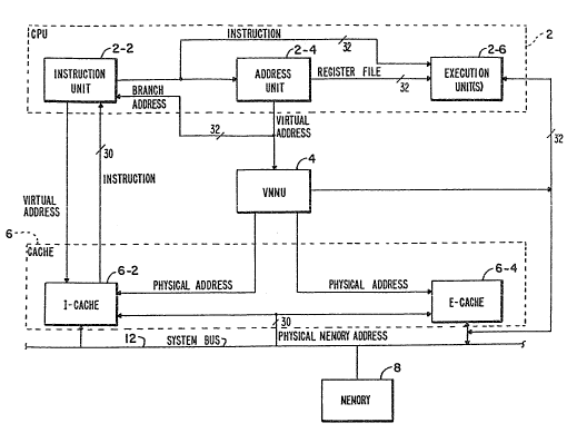
Figure 1 shc~ws a block diagram of a cycle
lo production pipleline data processing syst~m 1.
Included are a central processing unit (CPU) 2, a
virtual memory management unit tVMMU) 4, a cache unit
6, a memory subsystem 8, and input/output peripheral
unit lo. The cache unit 6, memory unit 8, and
input/output peripheral unit 10 are all coupl~d in
common to a system bus 12. The memory 8 stores
instructions and operands. Those operan~s and
instructions, having the highest probability of being
executed immediately, are traniferred to cache unit 6
from the memory subsystem 80
The CPU 2 r,eceive6 instructions from the cache
unit 6 and in the execution of these instructions
sends the virtual address portion o~ the instruction
to VMMU ~. The V~U 4 transl,ates the virtual address
i:nto a physical addreiss wh.ich is applied to cache
unit 6 ~or ~etchinij~ the neces,sary operands to allow
thle CPU 2 to execute the inst:ructions.
~ 37
The input/output unit 10 represents ~ypically
any number of peripheral controllers with their
devices, or an input/output processor which controls
peripheral controllers and devices, or it may
represent typic~l].y a communications subsystem.
Figure 2 shows in block diagram form the major
elements that make up the CPU 2 and the cache unit 6.
The CPU 2 includes an instruction (I) unit 2-2, an A
unit 2-4, and a number o~ ex~cution (E) units 2-6.
The execution units 2-6~ could be a scientific
instruction proces;sor or a commercial instruction - .
processor. However, for simplicity of description,
only the operation of one of the execution units 2-6 .:
is described whi.ch is sufficient to understand the .
invention.
The cache uni.t 6 includes an I-cache 6-2 and an
E cache 6-4. The I-cache 6-2 stores the instructions
that are to be exe~cuted and the ~-cache 6-4 stores
- the sperands upon which the instructions operate.
20 The I-unit 2 2 pexforms essentially two functions.
It prefetches ins~tructions from I-cache 6-2 and then
cracks those instructions to determine how the other
units, namely the A unit 2-4 and the E unit 2-6, will
further process th.e instruction.
25The A unit 2-4 receives the instruction from the
I-unit 2-2 and executes the instruction if it is a
register-to register instruction or a branch ~,~
~,, :,', ' , ''':' .' .'' .. -' . ' ' ' i , ., . .. , ,`" ,, . ' ,.
7~6~
9 .
inctruction. When the instruction is to be executed
by the E unit 2 6, the A unit 2-4 sends a virtual
address to the VMMU 4 which translates it into a
physical address for the E-cache unit 6~4. E-cache
5 6-4 sends the operands 1:o the E unit 2-6 for the
completion of the executio3n of the instruction
originally received by the :instruction unit 2-2 from
the I-cache unit 6-2.
The A unit 2-4 will also complete t~e execution
o~ branch i~struction and send the branch address
back to the instruction unit 2-2 so that it may
request the next instruction at the location in
I-cache 6-2 speci~ied by the bran~h address. Both
the A unit 2-4 and the E umit 2-6 include register
files which store the content~s of the registers which
are accessible to the programmers, that is, so called
software visible registers. ~B~th the I-cache 6-2 and
the E-cache 6-4 are coupled to system bus 12 and
their contents ar,e updated with instructions and
operands received from memory 8.
Instructions are executed in a production
pipeline fashion b~y the elemelts of CPU 2. That is,
the I unit 2-2 receives an :instruction from I-cache
6-2, cracks it, an~ then 6ends the instruction to ~he
A unit 2 4. Tlhe A unit ,2-4 either executes the
instruction or senl~s the virtual address to the VMMU
4 for translatioln in order to address the E-cache
7~7
.
--10--
6-4. E-cache 6-4 sends the clesignated operands to
the E unit 2-6.
While the A unit 2-4 is executing its portion o~
the first instruct:ion from the I unit 2-2, the I unit
2-2 is fetching the second ihstruction and subsequent
instructions from I-cache 6-:2. When the A unit 2~4
sends the virtua,l address speci~ied by the ~irst
instruction to the~ VMMU 4 and notifies the I unit 2~2
of that event, the I unit 2-2 sends the second
instruction to thel A unit 2~4. The VMMU 4 addresses
the E-cache 6-4 while the A unit 2-4 .is processing
the second instruction in the pipeline. When the E
unit 2-6 is executing the first instruction, the VMMU
4 may be addressin.g E-cache to fetch the operands of
the second instruction while the A unit 2-4 is
qenerating a .virtual address of th~ third
instruction. Meanwhile, the I unit 2-2 is cracking
the fourth instruction and ~etching one of the
subsequent instructions. Therefore, in this typical
example, there could be five instructions progressing
down the production line.
However, since the A unit 2-4 can execute
certain software visible reyister instructions, they
are removed ~rom the producition line as soon as the
execution o~ those instructio:ns is completed by the A
unit. Similarly, when the A unit 2-4 is processing a
branch instruction and the conditions o~ the branch
~3t~
are met, the A unit 2-4 imm~diately sends the bran~h
add~ess to the I unit 2-2 ancl that branch instruction
will be removed from the production line. This mode
and method o~ op~ratio~ results in increased
throughput as compared to the prior art.
Figure 3 shows in greater detail the elements of
the instruction unit 2-2, the A unit 2-4, the
execution unit 2-6 and their respective
interconnections. The P-counter 2-200 of the
instruction unit 2-2 is loaded by the A unit 2-4 with
a virtual address. This virtual address is the
address in I-cac:he 6-2 of the location of the next
instruction that i;s to be placed into the pipeline.
During the I-FETICH cycle, the virtual address is
lS transferred to I-cache 6-2 via an adder 2-202 and
either a register VA0 2-204 or a register VAl 2-206.
Either register VAID 2-204 or register VA1 2-206 is
used until a branch instruction is fetched. Then, if
rsgister VA0 2-204 is active, the address called ~or
by th~ branch insk:ruction would be stor2d in register
VAl 2-206.
The reason th~s branch adclress is held separately
in the VA0 2-204 and VAl ~-206 registers is because
if it is a conditional branch, the condition may ox
may not be met. I.e the condition is not met! then no
branch will result. This gives the system the choice
o~ either using or not using khe address called ~or
2~0'7~67
-12-
by the branch. The P counter 2-200, under ~irmware
control, is incremented by one for one word
instruction, incremented by two for a double word
instruction, or relplaced by ~i branch address.
The instruct.ion is read out of I-cache 6-2 into
either string buffers A 2-220 or string buffers B
2~221. Here again, one set of string buffers
receives successive instructions from I-cache 6-2
until there is a branch instruction. Then the
instruction following the branch instruction is
stored in buffers in the other string. For example,
if the ~tring buffers A 2-220 were being used then
the instruction ~ollowing the branch instructions
would be stored in the string buffers B 2-221. The ~::
throughput is ir~proved by storing ~oth sets of
instructions in case the hranch conditions are met
and the I unit 2-4 fetches the branch string from
string buffers B 2~221.
The instruction is read out of I-cache 6-2 into
either string buf~ers A 2 220 or ~tring buf~ers B
2-221. Here agaj.n, one set o~ string buffers
receives successi~e instructions from I-cache 6-2
until th~re is a, branch instruction. Then the
instruction following the branch instruction is
stored in bu~fers i.n the other string. For example,
if the string bu.f~ers A 2-220 were being used then
the ins~ruGtion ~ollowing the branch instructions
.
. , . . . . . . . . . . . ,,. . . ,., . ,- . . . ~ , , . , ,. ; . . . . ' . :
~ '7~
-13-
would be i~tored in the string bu~ers B 2-221. The
throughput i5 im;proved by ;~toring both sets of
instructions in case the branch conditi~ns are met
and the I unit 2-4 fetches the branch string from
string buffers B 2-221.
The instruction is then sent to the instruction
crack and resource control 2-210 which determines the
kind of instruction it is. That is, i~ this ls a
software visibl~ r,egister to register instruction,
lo then it wilI be exlecuted by the A unit 2-4 if it is a
memory instruction that will ble executed by the E
unit 2-6.
The instruction is sent from the crack logic
2~210 to an A-unit firmware address generator 2-208
which addresses 'an A-unit co:ntrol store 2-430. The
contents of the ad~ressPd location is stored in an
RDR (A~ register 2-406 in the A unit 2-4. The
instruction signal,s I INSTR 0-31 from ths string
~u~fers 2-220 o:r 2-221 are tra~sferred to the
instruction (RINST.R) register 2-400 in the A-unit
2-4. If the instruction is to be executed by the E
unit 2-6 it is also stored in an instruction first in
a first out register (FIFO) 2-600 in the E unit 2-6.
The instruction is also stored in an OP-CODE register
2-402 in ~he A unit 2-4 under control of a signal
I-BEGIN from the I unit 2-4. Both the RINSTR
register 2-400 and the OP CODE register 2-402 store
..... , .. , . . ., . , ,, ,, ,, , ., . . , .. , . . " . ., ", .,, , ~ j, ,,, , . ,., ; ~ j ; ,. , ~ . . . .
2~ 7~ 7
double words of 32 bits eii~ch.. If an instruction
requires 2 or 3 double words, then the OP CODE for
that instruction remains in the oP CODE register
2-402 while ea.~h of the double words of the
instruction in turn are stored in the instruction
register 2-400.
The output o~ the OP CODE register 2-402 is used
primarily for addressing a register file 2^-404 under
control of OP COD~ and firmware bits stored in the OP
CODE register 2-402 and the register RDR (A) 2-406
respectively. The register file 2-404 includes the
software visible registers. If the instruction being
executed is a memoxy instruction, then a virtual
address i5 generated and sent to the VMMU 4 via an
arithmetic logic unit (ALU) 2-412. Depending upon
the instruction being executed by the A unit 2-6, the
input to the ALU 2-412 may be applied to the A side,
by the RINSTR register 2-400, the OP CODE register
2-402, the register file 2-404 or a program counter
2-416. ALU 2-412 B æide inputs are provided by an
index shifter 2-410 ~or index or offset opPrations,
via an adder 2-408 or from register file 2-404. If
this is a registe:r instructioin, ~or example, a shift
operation o~ the contents oP a software visible
register in the rl~gister ~ile 2-404, then the output
o~ the register fi.le 2-404 may be applied to the
ishi~ter 2-414, be shifted the number of bits
2~ 7~j7
-15-
speci~ied by the i.nstruction and stored back in the
register file 2-404 in the same register from which
it was read.
For khe condi.tional bran~h instruction, signals
from RINSTR 2-400 and from the ALU 2-412 are applied
to branch logic 2-401. The output, load signal
A-P-LD, enables the P counter 2-200 to accept the
branch address signals A BRANCH which are sent to
I-CACHE 6-2.
When the A unit 2-4 has completed the execution
of the instruction, an A-DONE signal is sent to the
crack logic 2-210 o~ the I unit 2-2. This informs
the I unit 2-2 to send the next instruction stored in
the string buffers 2-220 or 2-221 to the A unit 2-4
and if required, to the E unit 2-6. If an
in~truction calls for execution by the E unit 2-6, ~.
then the I unit 2-2 sends that instruction to the
instruction FIFO 2-600 under control of ignal
I-ELAST and signal I-EFIRST. The ~ signals control
the loading of the instruction FIFO 2-600.
The I-BEGIN s.ignal is rec~ived by the ~ unit 2-4
when the CRACX signal is generated, the system is not
in a hold mode and no logic bll~ck including the clock
logic is itl a stal,l mode.
The CRACK sig~al is gene:rated when the ready
logic and flopl; 2-222 is ready to crack the
instruction, the sltring buf~ers A 2~220 or string
7~
--16--
buffers B 2-221 store at le.ar,t one instruction, and
the A unit 2-~ had generated the ADONE signal
indicating that the A unit is available for
processing the nex1t instruction.
The I unit 2-.2 generates lthe I-EFIRST and the
I-ELAST signals by the ready logic and flops 2-222 if
the instruction be.ing cracked .is to be executed by
the E unit 2-6. Both signa:ls are applied to the I
FIFO 2-600. The I--EPIRST signal enabl~s the I-FIFO
2-600 to store a d~uble word instruction. Th~ I-ELAST
signal enables the I-FIFO 2-600 to store a single
word instruction.
Note that the I unit 2-;2 sends the instruction
to be executed in 1:he A unit 2-4, and only to FIFO
2-600 if the ins1:ruction is 1:o be executed in the E
unit 2-6. In the E unit 2-6, the next instruction
the FIFO 2-600 will execute is applied to the next
address generator 2-602 which generates the E unit
control store 2-604 address :Location. The ~irmwar~
word is stored in a register RDR (E) 2-606~ The
instruction FIFO 2-600 stores up to ~our
instructions.
When the ~ uniLt 2-4 sends its virtual address to
the VMMU 4, the VM~ 4 g~nerat~l~ the physical address
which addresses th~ E-cache 6-~1. The contents of the
addressed locatiol~ is stored in a data FIFO 2-630 ln
the E unit 2-6 by ~;ignal LD-Dl~T-0015 ~or a single
. : . .: :. ., . : . . ......... - . . .
," ,, " ,, "" ,,,~ ",,, ,~" ,,, . , ,i,. . ., ,, . ~ .~ , ~, .; ; ; ~ ,...... ', ': ' '
7~7
-17
word transfer or signal LD-DAT 1631 for a double word
transfer. Signal LD-DAT-0015 also increments by one
the .FIFO 2-630 write addre~s to accept the second
word of the trans~er i~ ~he ~irst word was not at an
E-CACHE 6-4 word boundary. This data is the operands
on which the instruc~ion will operate. The E-unit
2-6 execu~es instructions whose operands are stored
in software visible regi~ters o~ register ~ile 2-630.
A typical instruction is the multiply instruction.
For this instruction, the A unit 2-4 generates a
dummy cycle by sending the virtual address
hexadecimal 40 to the '~MMU 4. This results in th~
E-CACHE 6-4 generating a dummy cycle by sending
signal LD-DAT 1631 to the FIFO 2-630 with a ~'dummy"
operand.
If in the I unit 2-2, the instructio~ calls for
a branch and has a displacement, then the
displacement from the crack unit 2-210 is applied to
the adder 2-202 to be added to the contents of the P
counter 2-200 and ;stored in either register VA0 2-204
or register VAl 2-:206 and applied to the I-cache 6-2.
~ multiplier 2-616 i8 cou]pled to the ~ ~ B ports
o~ register ~ile 2~-610 to g2~e:rate and store partial
products in conjunction wit~h the shifter 2-618 and
th~ Q-register 2~-620. The partial products are
applied to a rel3ult multip:lexer (MUX3 2-622 and
stored in accumulator locat;ion in register ~ile
!.,."' ~ ~, , .. ; .. " .... . . ' ' .' , ';
-18-
2-610. When the multiplication is compl ted th~
final result is stored in one of the software visible
registers of register ~ile 2-610.
A swapper logic 2-612 receives oper~nds from the
5 B side o~ regist~r ~ile 2-610 for swapping words
within double words and swapping bytes within single
words. A 16-bit word is made up of two 8-bit bytes.
A double word is made up o~ two 16-bit sin~le words
or four 8-bit bytes. A sign extender 2-614 repeats
lo the sign of all the high order positions of a double
word to the left o~ the first significant bit o~ the
double word.
The CTl and CT2 cow~ters 2~624 are used in the
calculation of the exponent of a floating point
resultant. A mantissa o~ a floating point operand is
processed through the ALU 2~608 and a shifter 2-618
in a conventional manner.
The software visible registersi in both the
register files 2-404 with A unit 2-4 and 2-610 in the
E unit 2-6 are updated on successive cycles so that
they both contain th~ same information. This is
accomplished by firmware signals from register RDR
(A~ 2-406 which are applied to logic 2-420 to
generate an update siqnal A-UPDT which enables the
register file 2-~10 and six A-ADR signals which are
applied to the address terminals of register ~ile
2-610 to store the data ~rom the D terminal o~ the
--19--
register file 2-404 to he D terminal of register
file 2-610. Similarly, the E-UPDT signal from
register RDR tE) 2-606 enable register file 2-404 to
store the data at the addres~s specified by signals
5E-ADR from logic 2-601. :Lo~ic 2-601 sig~als E-ADR
from instruction signals from the instruction FIF0
2-600 and firmware signals f:ro~ RDR (E) 2-606.
The A unit 2-4 program count~r 2-416 stores the
address of the next instruction. P counter 2-200 in
the I unit 2-2 ,also stor~s the address of the next
instruction. The :reason for the two regist~rs is
that, in case O:e a condit.ional branch, P counter
2-200 in the I unit 2-2 stores the branch address in
case it is to be used, whereas the program counter
2-416 will not store the branch address but stores
the nexk address in the sequence presently being
Pxecuted.
~ eferring nexl_ to Fig. 4, the components of the
E-cache unit 6-4, necessary for understanding the
present invention, are illustrated. An address
associated with ~In instruct:ion is transferred from
the address unit 2--4 to the V~ unit 4 wherein the
vi:rtual address (from th~ address unit 2-4) is
translated into a real address" The real address is
entered into the real address register 6-401. In the
prior art, the address of the real address register
is applied to ~he tag directory unit 6-403 and when
--2 O--
the tag directory unit 6-403 stores the applied
address along with a "valid" ;signal (indicating that
the associated operand is not compromised), then a
"hit" signal is generated and, ~or a read
instruction, the o;perand in thle storage unit 6-404 at
a location associated with the address in the real
address register 6-401 is ~ransferred to ~he
execution unit 2-6 via data out register 6-411. When
the address in th~ real addresls register 6-401 is not
stored in the tag directory un.it 6-403 or the address
is stored but a "valid" s.ignal is not present
therewith, then a "miss" signal is generated. For a
read instruction, the address in the real address
register is enta:red in the miss register 6-402,
applied to the bus int~rface unit 7 and applied,
along with control signals, to the system bus 12.
The requir~d opera~ld is retrieved from the memory
unit 8 and tran~ferred via system bus 12, bus
interface unit 7 and bus data .in register ~408 to
the storage unit 6-404 where the operand is stored at
a location determilted by the address in the real
address register 6~401. The "valid" signal is stored
in an associated location in the tag directory uni~
6-403. When the "miss" signaL is present (i.e., the
"hit" signill is not present) and a write instruction
is associated wil;h the addr~3ss in the real address
register 6--401, the~n an operan~1 from the execution
. ... ... -, ~
-21-
unit is applied to the system bus through the data in
register 6-409, the bus data out register 6-410 and
the interface unit. This write instruction operand
i5 applied to the system bus along with the write
operand address from the rea]. address register 6 401
and the write operand is stored in the memsry unit 8
at a location determined by the write operand
address. When the: "hit" signal is present for a
write instructiorl, the operand is also stored in the
storage u~it 6-404, at a locati.on determined by the
address in the real address register 6-401. The
automatic storage o~ a write operand in the memory
unit 8 is reEer. red to as write-through or store
through cache str2~tegy.
In the present invent:ion, a wrike address
register 6-421 i.s provided 5iO that additional cache
activity can be accomplish~!d while the write
instruction operalnd, associat:ed with a write operand
address in the wri.te address register 6-421 can be
determined. In addition, when the address in the
real address regis,ter 6-401 is being transf~rred ~o
the write addres~s register ~i-4 21, the write operand
address is appliedl to the tag directory unit 6-403.
~hen the applicat.ion o~ the write operand address in
the real address register 6-401 to the tay directory
unit 6-403 produc~!s a "hit" si.gnal, a "hit" signal is
stored in a locati.on 6-421A associated with the write
.
~0~7~i7
-22-
operand address.
The E-cache unit 6-4 of the present invention
includes a block store ram 6-420. When the address
in the real address register l5-401 is trans~erred to
write address register 6-421, khe address is stored
in the block store ram 6-420. The block store ram
6-420 has the propexty that, when the same address is
applied to the block store ram as is stored in the
block store ram, a "busy" signal is generated. The
"hit" signal and the "busy" signal are used as
control signals in the present invention to control
processin~ activity in the E-cache unit 6-4.
Re~erring next to Fig. 5, the operation of the
present invention ils illustrat~d by means of a flow
diagram. In step 501, a next s;equential address from
the first-in, ~irst:-out (fifo) register of VMMU 4 is
entered into the real address, register 6-401 of the
execution cache unit 6-4. In step 502, a
determination is made whether the address entered in
~0 the real address register 6-401 is associated with a
read instruction or a write instruction. When the
address is associated with a read instruction, the
read instruction procedure is executed by the
execution cache unit in ~tep 503 and a next address
~rom the VMMU 4 is entexed in the real address
regi ter 6-401 in step 501. When the address in real
address register 6-401 is associated with a write
2~ 71~;~
-23-
address in step 502, then the c:ontents of the real
address register 6-401 are applied to the tag
directory unit 6-403 and a cletermination is made
whether the tag di.rectory unit: 6-403 has the applied
address stored therein a1Ong wi.th a "valid" status
signal in step 504. When the tag directory unit
6-403 does not store the app1ied address along with a
"valid" status siqnal, then the contents of the real
address register are stored i.n the write address
register without a l'valid" signal stored in the
1Ocation 6-421A. When, in st:ep 504, the applied
address and a "va1i.d" status si.gnal are present, the~
the address irl the real addres~s register 6-401 is
stored in the write address~ register 6-421 and a
"valid" signal i.s stored in the write address
register location 6-421A in s,tep 507. In step 508,
the address from thle real addre!ss register 6-401 are
entered in the block store ram 6-420. In step 509, a
determination is made whether t.he write operand is
available, i.e., is the E-MWRITE signal ~rom the
execution unit present. When t.he E-MWRITE signal is ~
present, then, inl step 510, the address from the - :
write address regi.ster 6-421 and the associated
operand ~rom the execution unit 2-6 are applied to
the bus inter~ace unit. In step 511, when the
"va1id" signal iSI present in the write address
register 6-421, thel contents o~ the write address
~,,
-24-
register 6-421 are applied to the storage unit 6-404
and the associated operand from the execution unit
2-6 is stored at the addressed location in tha
storag~ unit 6-404. In step 5.12, the "busy" signal
(and associated address) are removed from th~ block
store ram 6-420 and the next address ~rom the VMMU 4
is stored in the r~eal address :register. When, in step
509, the associated operand is not ready from the
execution unit 2-l6, then the mext address is entered
from the VMMU 4 in the real address register 6-401 in
step 513. In step 514, a dete.rmination is made as to
whether the address in the reaL address register is a
read instruction or a write instruction. When the
address in the rea:L address r~gister is associated
with a write instruction, then the address is held in
the real address .register 6-~01 until the "busy"
signal is removed fxom the block store ram in step
516. When the "busy" signal is removed ~rom the
block store ram 6-420, then the contents of real
address register 6-401 are applied to the tag
directory unit S--403 to determine if the identical
address is stored ;llong with a "validl' signal in step
504. When, in step 514, lthe address in the read
address register is assoc.iated with a read
instruction, then the address in the real address
register 6-401 is ;~pplied to the block store ram
6-420 arld a dete~mination is mada in step 517 as to
-25-
whether the address of the real address register
reserved by the i~ddress stor,~d in th~ write address
register 6-421 as indicated b~y the presence of a
"busy" signal from the block store ram ~-420. When
tha block store ram 6-420 prov.ides a "busy" signal,
then the address in the real instructio~ register
6-401 is held therliin in step 521 until the "busy"
sign~l from the block store :ram 6-420 is removed in
step 522. When th/_ "busy" s:ignal from the block
lo store ram 6-420 .is removed, lthen the read procedure :
is executed in stel? 519 and a next address i~ entered
into the real a~1dress register 6-401 in step 501.
When, in step 517, the block s~ore ram 6-420 does not
provide a "busy" s.ignal, then the address in the real
address register 6-401 is applied to the tag
directory unit 6~-403 to determine if the address
stored in the real address reg:ister 6-401 is stored
along with a "valid" signal in the tag directory unit
6-403 ln step 518. When the address in the real
address register 6~-401 is stored along with a "valid"
signal in the tag directory un:it 6-403, then the read
instruction procedure for the cache memory unit is
executed in step 5:l9. When, in step 518, the address
stored in the real address register 6-~01 and an
associated "valid" signal are not stored in the tag
directory unit 6-403, then lhe address in the real
address reqister 6--401 is held therein in tep 5~0
7~t-~7
26-
until the "busy" signal is removed in step 522. ~he
read procedure associated with. the address stored in
the real address reyister is execut~d in step 519.
2. Operation of t~e Preferred Embodiment
The present invention provides a technique for
using the time between the completion o~ a write
instruction operand addre~s ~y th~ VMNU unit and the
completion of the preparation of the write
instruction operand. The present invention provid~s
for the storing ~f the write instruction operand
addresis along with an indicia indicating the presenc~
of a valid operand at the location determined by the
write instruction operand address. In the present
invention, a read in truction can be processed by the
E-cache unit when the r~ad instruction operand
address does not con~lict with the stored write
instruction operand address and when the valid read
instruction operand i5 stored in the E-cache. The
conflict between the read instruction operand address
and the write instruction operand address is resolved
by the presence of the "busy" sig~al from the block
store cache unit. The "bu~y" signal maintains the
reiad instruction address in the real address register
until the write operation is processed by the E-cache
unit and th~ l'busy" signal is removed. Similarly,
when the read instruction address operand is not
stored in the tag directory unit along with a "valid"
'7
~ 27-
signal, the missing operand must be retrieved ~rom
~he memory unit. This operand retrieval can conflict
with the write instruction still pending in the
E-cache unit and, therefo:re, th~ read instruction
operand address is stored in the real address
register without further intleraction with the E-cache
unit until the pending w:rite instruction is
completely processled and the "bu~y" signal is removed
from the block sto:re ram. The processing of the
pending write instruction includes the storage o~ the
write instruction operand in the ~ache unit when the ~ :
"valid" bit is st:ill present after completion of the
write instruction operand.
As will be clear to those skilled in the art,
the flow diagram O~e Fig. 5 is n~eant to illustrate the
operation of the pr.ese~t invention and is not meant
as representation of actual apparatus. For example,
many of the decision steps can be implemented by
switches respondinsl to control signals rather than by
20 a logical decision network. Si.milarly, in Fig. 4, .-
many of the cont:rol signal paths that are used to .. ~.
implement a cache unit in the prior art have not been
illustrated to emphasize the operation o~ the present .-
invention.
The foregoirlg description is included to
illustrate the opeiration of the pr~erred embodiment
and i~ not meant tCI limit the scop~ of the invention.
X~'7~,7
-28-
The scope .of the invention is to be limited only by
the following claims. From the foregoing
description, many variations will be apparent to
those skilled in the art that would yet be
encompassed by the spirit and scope of the invention.