Note: Descriptions are shown in the official language in which they were submitted.
~ ~ ~ 7 ~ 7 ~
,
RELATED PATENTS
Canadian patent No. 2,007,004 of Edward F. Getson,
Jr., John W. Bradley, Joseph P. Gardner and Alfred F. Votolato
entitled, " Multiprocessor Controller Having Shared Control
Store," lssued June 7, 1994 which is asslgned to the same
assignee as this patent applicatlon.
United States patent No. 4,888,727 of Edward F.
Getson, Jr., John W. Bradley, Joseph P. Gardner and Alfred F.
Votolato entltled, "Peripheral Controller with Paged Data
Buffer Management," issued December 19, 1989, which is
asslgned to the same assignee as this patent appllcatlon.
72434-104
20(~7376
~_ -2 -
BACKGROUND OF THE INVENTION
Field of Use
This invention pertains to data processing systems
in which a system bus network is shared by a plurality
S of units and more particularly to a method and
apparatus for limiting the use of such system bus
network.
Prior Art
In many data processing systems, a bus network is
frequently used to interconnect the different element~
together. In certain types of these systems, the
access of one or more master controllers to the bus
network is controlled through a single bus arbitration
module which grants access to the master controllers on
a priority basis. The bus master granted access
performs the specified request which, in certain
instances, involves the performance of burst type
transfers. Depending upon the types of requests being
performed by the plurality of master controllers, the
system's central processing unit, normally granted low
priority, has been effectively precluded from using the
bus network.
To prevent this, the system disclosed in U.S.
Patent No. 4,719,567 includes apparatus within the bus
master controller which limits its activity during a
particular time interval based upon the bus activity
during a preceding time interval. However, the
arrangement requires a centralized arrangement which
operates in a synchronous manner. Also, the
;Zn(l 7376
- 3 -
arrangement determines the activity of the bus by
dividing the activity of the bus master controller into
a succession of sample intervals comprising a selected
number of clock cycles of the bus master controller.
During each such sample interval, the bus master
controller determines the utilization rate of the bus
network as the ratio of the number of clock cycles
during which the grant acknowledge signal of such
controller is active to the number of clock cycles
comprising the sample interval. If the utilization
rate of the bus network during a particular sample
interval is determined to be above a selected
threshold, the bus master controller is prevented from
arbitrating for the use of the bus network during the
lS next successive sample interval. If the utilization
rate is determined to be below the predetermined
threshold, the bus master controller will be allowed to
contend for the right to use the bus network. This
form of measurement involving measuring ratios of
intervals has been found somewhat ineffective in that
it reduces system performance.
Also, the system of U.S. Patent No. 4,558,428 is
of interest in that it discloses how a high priority
unit, such as a memory controller, during the execution
of a burst type transfer operation which could saturate
an asynchronous bus network, is able to skip a cycle of
the burst type transfer operation, enabling a lower
priority unit access to the memory controller's
memory. While this arrangement improves overall system
performance by enabling a lower priority unit access to
memory, during a burst type transfer, it does not
prevent the bus network from being saturated by other
units competing for bus network access.
Z007376
~ .
Accordingly, it is a primary object of the present
invention to provide a method and apparatus for
limiting the utilization of an asynchronous bus system
by a user bus unit.
It is a more specific ob~ect of the present
invention to provide a method and apparatus for
limiting access to an asynchronous bus network by any
one of a plurality of units connected to the network
which are granted access by priority logic network
distributed among such units.
SUMMARY OF THE INVENTION
The above and other ob~ects of the present
invention are achieved by the preferred embodiment
which includes a plurality of units which are coupled
to transfer requests, and data over an asynchronous bus
network during allocated bus transfer cycles. Each
unit has a common interface portion which includes bus
request circuits and response circuits for
acknowledging requests received from other units.
A tie-breaking bus priority network i8 di~tributed
to the common interface portion of each of the
plurality of units which grants bus cycles and resolves
simultaneous requests on a priority basis. In general,
priority is granted on the basis of the unit's physical
position on the bus network. In the system of the
preferred embodiment, the highest priority is given to
the system's memory subsystem and the lowest priority
to the system's central processing unit with the other
units being positioned on the basis of their
performance requirements.
2~07376
-5-
According to the teachings of the present
invention, at least one unit, such as a disk type
peripheral controller subsystem, includes bus
saturation detection apparatus within the common
interface portion for monitoring bus activity.
Activity is monitored by detecting the absence of
unused bus cycles occurring over a given interval of
time. The detection of the occurrence of one or more
available cycles over the given interval of time is
used to signal that the bus network i8 not in a
-~aturated state. However, when the presence of at
least one unused or available bus cycle i8 not
detected, this signals that the bu~ network is
saturated.
In more particular terms, the peripheral
controller subsystem includes a microprogrammed
processor which sets an indicator within the bus
saturation detection apparatus to a predetermined state
under microprogram control at the beginning of a
transfer operation interval. The detector monitors the
state of at least one predetermined signal utilized by
the bus priority network for determining the extent of
bus utilization. The detector apparatus switches the
state of its indicator upon detecting the occurrence of
an unused or available cycle. The output of the
detector indicator is provided to branch test circuits
included within the processor. At the end of the
transfer interval, the subsystem tests the state of the
saturation detector indicator. If the detector
indicator specifies that the bus is not saturated, it
resets the state of the indicator and begins another
interval.
7 ~
~ " .
This process continues wlth the perlpheral
controller perlodically clearlng the state of the saturation
detector indicator and determlnlng if lt is stlll ln the
predetermlned state. When the lndlcator speclfles that the
bus network ls saturated, the perlpheral subsystem throttles
down lts operatlon by lncreaslng the amount of tlme between
lssulng requests. In the preferred embodlment, thls ls
accompllshed by addlng or lncrementlng a "walt count value."
Addltlonally, the processor can also ad~ust lts
operatlon by alterlng or changlng lts prlorlty from hlgh to
low as a functlon of the results of testlng for bus
saturatlon. Thus, processor can be easlly programmed for
malntalning a desired transfer rate requlred for efflclent
operatlon.
In accordance wlth the present invention there is
provided bus saturatlon apparatus for detectlng saturatlon on
an asynchronous bus network coupled ln common to a plurallty
of data handllng unlts durlng the asynchronous transfer of
data between different ones of said units durlng bus cycles of
operatlon granted on a prlorlty basls controlled by a priorlty
network lncluded as part of sald bus network, sald prlorlty
network belng dlstributed to each of said plurality of units,
said bus saturatlon apparatus belng lncluded ln at least one
of said units, said apparatus comprlslng: means coupled to
sald bus network for monltorlng the state of a predetermlned
one of a number of lines of sald bus network lndlcatlve of bus
actlvlty; and, blstate lndlcator means coupled to sald
72434-104
7 ~
' .~
monitorlng means, said lndlcator means belng set to a
predetermlned state at a start of a data transfer interval by
sald one unlt and said bistate indicator means being switched
to another state by said monitorlng means when sald monltorlng
means detects that sald bus network ls not belng saturated.
In accordance wlth the present lnventlon there ls
further provlded a perlpheral controller for controlllng the
high speed transfer of data from at least one input/output
devlce to and from an asynchronous bus network whlch connects
said controller common wlth a plurallty of data handllng units
for asynchronously transferring data between different ones of
sald units during bus cycles of operation granted on a
priorlty basls controlled by a priority network lncluded as
part of sald bus network, sald prlorlty network belng
dlstrlbuted to each of sald plurality of units, sald
controller comprlslng: a bus saturation detector coupled to
said bus network sald detector includlng: means coupled to
sald bus network for monltorlng the state of a predetermlned
one of a number of llnes of sald bus network lndicatlve of bus
activity; and, a bistable indlcator coupled to sald monltorlng
means, sald blstable lndlcator belng switched from a flrst
state to a second state by said monitoring means when said
monltorlng means detects that sald bus network ls not belng
saturated; and, processor means for generatlng slgnals for
transferring blocks of data between sald lnput/output devlce
and sald bus network, sald processor means belng coupled to
sald bus saturatlon detector, sald processor means settlng
~- 6a
~, -
72434-104
~ 7 3i7 ~
sald indicator to said first state at a start of a data
transfer operation interval and sald processor means including
means for testlng said state of said lndicator at a completion
of said data transfer operation interval.
In accordance wlth the present lnventlon there ls
also provided a method of preventing the saturatlon of an
asynchronous bus network coupled ln common to a plurallty of
data handling unlts in which data ls asynchronously
transferred between dlfferent ones of sald unlts during bus
cycles of operation granted on a priority basis controlled by
a priority network lncluded as part of said bus network, sald
priority network being distributed to each of said plurality
of units, said method comprising the steps of lncludlng as
part of a bus lnterface of each of a number of sald unlts, a
bus saturatlon detector clrcult; monitorlng bus cycle activlty
by connectlng an lnput of sald bus saturatlon detector to a
predetermlned llne of said bus network; setting said detector
clrcuit to a flrst state at the start of a data transfer by a
processor lncluded ln sald each of a number of unlts;
switchlng sald detector clrcult from sald flrst state to a
second state when sald detector clrcult detects an occurrence
of an unused bus cycle; testlng the state of said detector
clrcuit at the end of said data transfer interval by sald
processor for determining if sald bus network ls being
saturated; and, throttling down the rate at which data is
being transferred by said processor ln a predetermined manner
when the state of said detector circult lndlcates that sald
bus network ls saturated untll sald bus network ls no longer
6b
~,
- 72434-104
~Q ~7~7~
being saturated.
In accordance with the present lnvention there ls
further provided an apparatus for detecting saturation of a
system bus by one of a plurality of data handling units, said
bus being of the type wherein said plurality of data handling
units are coupled to said bus for participating ln operations
in which data is transferred over sald bus between palrs of
said units and whereln each of sald units can lnltlate such a
data transfer operation by generating a slgnal requestlng the
use of the bus for a data transfer operation; sald apparatus
being characterized by; a monltor circuit coupled to monitor
said bus and for generating an output signal in either one of
first and second states, said first state representlng that
sald bus is busy carrylng out a data transfer operationi a
signal generator circult for generating a signal when said one
data handling unit inltlates a request for use of sald bus; a
fllp-flop, operable in elther one of first and second states,
sald flip-flop being coupled to sald signal generator circult
and responsive to sald slgnal generated thereby for switching
to the first state thereof, said flip-flop belng coupled to
said monitor circuit and responsive to the second state of the
output signal generated by said monltor clrcuit for switching
to the second state thereof; and a detector circult coupled to
said fllp-flop for sensing the state of operation thereof and
for deliverlng a slgnal representlng the contlnuous use of
said bus by said one unit during a predetermined interval
indicative of a saturation condition.
The novel features whlch are believed to be
6c
72434-104
7 ~
"".,
characteristlc of the invention both as to its organization
and method of operation, together with further obiects and
advantages, will be better understood from the following
description when considered ln connection with the
accompanying drawings. It is to be expressly understood,
however, that each of the drawings is given for the purpose of
illustration only and is not intended as a definition of the
limits of the present invention.
BRIEF DESCRIPTION OF THE DRAWINGS
Figure 1 is a block diagram of a data processing
system which includes the apparatus of the present invention.
6d
73434-104
zno7376
-7 -
Figure 2 shows in greater detail, the peripheral
subsystem of Figure 1 which includes the apparatus of
the present invention.
Figures 3a and 3b show in greater detail, the
subsystem of Figure 2.
Figures 4a and 4b show the format of a
microinstruction and arrangement of microinstructions
included within the subsystem of Figure 2.
Figure 5 is a flow chart used to explain the
operation of the present invention.
DESCRIPTION OF SYSTEM OF FIGURE 1
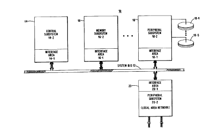
Figure 1 shows a data processing system 10 which
include~ a plurality of subsy-~tems 14 through 20 which
couple in common to an asynchronous system bus network
12. The illustrative subsystems include a central
subsystem 14, a memory subsystem 16, a disk peripheral
subsystem 18 and a local area network subsystem 20.
Each subsystem includes an interface area which enables
the unit or units associated therewith to transmit or
receive requests in the form of commands, interrupts,
data or responses/status to or from another unit on the
system bus 12 in an asynchronous manner.
By way of illustration, only four subsystems are
shown in Figure 1. However, the data processing system
normally includes additional subsystems for
connecting a full complement of peripheral devices,
other processing units and communication devices to
system bus 12. While each of the interface areas of
the peripheral subsystems can include the apparatus of
the present invention, it will be assumed that only
Z007376
8 -
interface 18-1 of subsystem 18 includes such
apparatus. Therefore, only subsystem 18 will be
described in detail herein with reference to Figure 2.
DESCRIPTION OF PERIPHERAL SUBSYSTEM 18
Referring to Figure 2, it is seen that disk
peripheral subsystem interface area 18-01 includes a
section 18-10 which includes the bus driver and
receiver circuits of block 18-12, the di6tributed
system priority network and bus request logic circuit~
of block 18-14 and the bus saturation detector circuit
of block 18-16. The circuits of block 18-14 and 18-16
couple to system bus 12 via the driver and receiver
circuits of block 18-12.
The peripheral subsystem 18-2 includes a pair of
processors 18-20 and 18-22 which operate under the
control of sequences of microinstructions stored in a
control store unit 18-24. The processor 18-20 handles
those tasks involving the subsystem-~ystem bus
interface, such as transfers commands, data, etc.,
while processor 18-22 handles those tasks involving the
subsystem-device interface. Both processors share a
scratchpad memory and data buffer memory included as
part of the subsystem memory unit 18-26. The
scratchpad memory includes register locations used for
storing device parameter information in addition to
providing temporary storage for control and data
handling operations (e.g. status and address
information). The data buffer memory stores different
blocks of data bytes being transferred across both the
system and device interfaces.
3 7 6
The peripheral subsystem 18-2 also includes the
devlce interface circuits of block 18-28. These circuits
establish an interface with the disk storage devices 18-4 and
18-5 of Figure 1 for controlling device operations and
generating the required dlalogue sequences over the associated
device level interface. In a preferred embodiment, the device
level interface is a SCSI (Small Computer System Interface)
devlce. This type of interface is described in an artlcle
entitled, "Adding SCSI to the SB180 Computer, Part I
Introduction" by Steve Ciarcla, published in the May 1986
issue of Byte magazine. For further information regarding the
operation of the different blocks of Figure 2, reference may
be made to the related patents.
The details of processor 18-20 will only be
described to the extent necessary to understand how it
utilizes the method and apparatus of the present inventlon.
Briefly, processor 18-20 includes an ALU (Arithmetic And Logic
Unit) sectlon 18-200, an instruction register and decode
section 18-210, and a test multiplexer and microsequencer
logic section 18-220. The ALU section 18-200 ls capable of
performing logical and arithmetic operations on A and B
operand signals received from several sources includlng
scratchpad memory and section 18-220. These operations are
performed under control of microinstructions loaded into an
instruction register of section 18-210 from control store 18-
24. The ALU, after performing the speclfied operatlon,
delivers the result via an output register to several units
72434-104
~ ~7 .~7~
includlng scratchpad memory and to the bus request logic
circuits of interface 18-10.
9a
72434-104
Z0~7376
""~ --10--
The instruction register and decode ~ection
18-210, as shown, includes the instruction register for
storing each microinstruction read out from control
store 18-24, during a processor cycle of operation.
5The different fields are decoded and applied as inputs
to a number of test multiplexer circuits which, in the
case of certain types of microinstructions (e.g.
branch), enable the microsequencer logic circuits to
generate the address of the next microinstruction to be
10read out of control store 18-24. Certain portions of
these circuits will be described in greater detail
relative to Figure 3b.
DETAILED DESCRIPTION OF FIGURE 2 CIRCUITS
Figure 3a shows in greater detail, the distributed
15system priority network and bus request logic circuits
of block 18-14. As shown, these circuits transmit and
receive signals to and from asynchronous system bus
network 12 via the driver and receiver circuits of
block 18-12. One first such signal is bus data cycle
20now signal BSDCNN+10. This signal is passed through a
60 nanosecond delay line 18-140. The sixty (60~
nanosecond period enables the highest priority
requesting unit to utilize the next bus cycle without
interference. At the same time, the receiving unit or
25slave uses this signal as a synchronizing signal.
The resulting output signal BSDCND+OO and signal
BSDCNN+10 are logically combined in a first OR gate
18-141 which produces a strobe signal BSDCNB+OO. This
signal is used to clear the distributed priority
30network between system bus cycles. An OR gate 18-142
combines output signal data cycle now busy signal
~ fl ~ ~7 ~
.,,=.
BSDCNB+00 with the high level and low level bus request
signals BSREQH+00 and BSREQL+10 recieved as output bus request
signal BSREQT-10 from a NOR gate 18-144 as shown.
The slgnal BSDCNB+00 filters out from the resulting
output signal PRIBSY-00 any mornentary glitches appearing on
the bus request leads since signal BSDCNB+00 is high during
the interval during which the signals applied to these leads
change state. Thus, signal BSDCNB+00 bridges any hole
occurring between successive user requests.
When signal BSREQT-00 switches from a binary ONE to
a binary ZERO, lt causes an OR gate 18-142 to force priority
busy slgnal PRIBSY-00 to a binary ZERO ln the absence of
slgnal BSDCNB+00. Signal PRIBSY-00 remains a binary ZERO
until slgnal BSDCNB+00 is forced to a binary ONE. The signal
PRIBSY-00 defines when the distributed priority network of bus
12 swltches from an ldle state to a busy state. That is
prinet slgnal PRIBSY-00 ls applied to a twenty (20) nanosecond
delay llne 18-143 which generates as output signals PRIBSY-20
and PRIBSY-40. That is, prinet busy signal PRIBSY-00 is
applied to a twenty (20) nanosecond delay line 18-143 which
generates as outputs signals PRIBSY-20 and PRIBSY-40. The
signal PRIBSY-20, when a binary ZERO, prevents the storage of
any request generated by processor 18-20 during a priority
network resolutlon cycle.
The signals PRIBSY-20 and PRIBSY-40 are combined
wlthin a NOR gate 18-145 to produce signal PRIBSY+50 which is
applied as one lnput to a NAND gate 18-149 which determines
~:~a 1 1
.~
72434-104
7 ~ 7 ~
.~
whether o~ not subsystem 18 ls to be granted access to system
bus 12.
lla
72434-104
Z0~7376
-12-
The series connected NAND gate 18-146, D-type
grant flip-flop 18-147 and NOR gate 18-148 are used to
generate my request signal MYREQT+10 in response to
peripheral subsystem 18 requesting access to system bus
12 (i.e., signal CYCREQ+00=1). The my request signal
MYREQT-00 is applied as one input to NOR gate 18-148
which receives as a second input, a high priority
request signal HIREQT+00. In the absence of a high
priority request (i.e., signal HIREQT+00=1), processor
request signal MYREQT-00 causes NOR gate 18-148 to
force request signal MYREQT+10 to a binary ONE. The
NAND gate 18-149 also receives as inputs, the
distribution priority network signals BSBUOK+00 through
BSGUOK+00 which correspond to those of the subsystems
positioned at higher priority positions on sy~tem bus
12. In the absence of any higher priority subsystem
request, NAND gate 18-149 forces set data cycle now
Rignal SETDCN-00, to a binary ZERO. This, in turn,
forces my data cycle now D-type flip-flop 18-150, to a
binary ONE. The receipt of any response from a syRtem
bu~ 12 causes a NOR gate 18-154 to generate a reset
signal CLRDCN-00.
The NAND gate 18-151, driver circuit 18-152, and
D-type flip-flop 18-153 are used to generate high
priority request signal HIREQT+00 for indicating the
presence of a high priority request signal, in response
to signal HIREQS-00 generated in response to a high
priority request from system bus 12. Signals
MYHPRI+00, MYHPRI-00 and MYREQT+00 cause a pair of AND
gates 18-155 and 18-156 to generate high and low
priority request signals MYREQH+00 and MYREQL+00.
These signals are applied to system bus 12 via the
driver circuits of block 18-12.
Flgure 3b shows in greater detail, the bus
saturatlon detector 18-16. As shown, the detector recelves
bus data cycle now busy signal BSDCNB+00, from the circuits of
block 18-14 which is applied to an OR gate 18-160. The
resulting signal REQDCN+00 ls applied to the lnput of a delay
line 18-161 and to one input of an OR gate 18-162
The signal REQDCN+00 is delayed by a predetermined
amount and then applled as slgnal RQDCDL+00 as a second lnput
to OR gate 18-16Z. The predetermined amount of delay is
selected by measuring the delays incurred by bus data cycle
now signal BSDCNN+10, and bus acknowledgement signal BSACKR+10
shown ln Flgure 3a. The value is chosen so that the slgnal
BCYSMP+00, produced by loglcally comblnlng signals REQDCN+00
wlth RQDCDL+00 ln an OR gate 18-162, remalns constantly on
during the period of tlme that system bus 12 is saturated.
This value approxlmates 150 nanoseconds.
As seen from Flgure 3b, signal BCYSMP+00 is applied
to the reset or clear input terminal of D-type bus saturation
detector indicator flip-flop 18-163. The preset input is
connected to receive a sample control signal SMPLBS-00 from
processor 18-20. When forced to a binary ZERO, this signal
switches flip-flop 18-163 to a blnary ONE state. The binary
ONE output signal BUSSAT+00 is applied as an input to one of
the test conditlon multiplexer circults of block 18-220.
Also, Figure 3b shows in greater detail, certain
processor decoder and test circuits. It ls seen that the
processor decoder circuits 18-210 include a pair of decoder
clrcuits 18-21Oa and 18-21Ob which are used to decode
72434-104
7 ~
",...
specified flelds of a microinstruction which results in the
generation of sample control signal
13a
72434-104
7 ~
~.""j,",, 7
SMPLBS-00. The processor test condition multiplexer circuits
of block 18-220 include a test conditlon multiplexer circuit
18-221 which, in response to one of the control fields of a
test and branch type microinstruction of Flgure 4a, selects
one of eight possible output conditions to select. The
selected output condition signal BTSTMX-00 is compared by an
exclusive OR gate 18-222, and the result is stored in a branch
test enable D-type flip-flop 18-224. The output signal
BTSTCN-00 is applled as an input to the processors's micro-
sequencer logic circuits.
One of the input signals whose state is tested by
circuit 18-221 lncludes signal BUSSAT+00. As shown, thls
signal is applied as one of the inputs to a multiplexer
circult 18-223. Another field of the test and branch
microinstruction of Figure 4a is used to select which one of
the test inputs will be selected for testing. The output of
multiplexer circuit 18-223 which corresponds to signal
BLUAX6+00 is also applied to the ALU as signal BAOPB6+00.
MICROINSTRUCTION FORMAT
Figure 4a illustrates the format of the test and
branch microinstruction used in con~unction with the present
invention. Bits 0-1 are used to specify the type of micro-
instruction. These bits are "10" in the case of the test and
branch microinstruction.
Blt 2 is a single bit field whose state specifies
when the scratchpad memory is to be enabled. Bit 3 is a test
field bit which is set to a ZERO value and used to test the
14
72434-104
_ ~ lJ fl 7 ~ 7 ~
state of a signal selected for testing. The bits 4-6 are a
multiplexer test conditlon fleld.
14a
.,
72434-104
Z007376
15-
There are up to eight multiplexer circuit outputs which
can be tested using TFZ bit 3. Bits 7-10 are an AOP
field used in con~unction with bit 2 to select which
input to the multiplexer circuits is to be tested.
Must be zero (MBZ) bit 11 is set to ZERO. Bits 12-23
are an 12-bit branch address which is used as a next
address when the condition being tested is true.
DESCRIPTION OF OPERATION
With specific reference to the flow chart of
Figure S, the method and operation of the bus
saturation detector apparatus of the pre~ent invention
will now be described with reference to Figures
throuqh 3b and 4a. Initially, the peripheral subsystem
will be configured or initialized to operate at maximum
efficiency or performance. For example, it is assumed
that it will be operating as a high priority device
established by the setting of a register bit.
In this example, processor 18-20 issues successive
memory read requests, each coded to specify a burst
transfer. In response to each such request, memory
subsystem 16 transfers a number of double words of data
over a number of successive bus cycles in that, memory
subsystem 16 has the highest priority access. This
type of operation is most likely to result in the
saturation of system bus 12. While the arrangement of
U.S. Patent No. 4,558,429 can to some extent alleviate
thi~ condition relative to certain types of transfers,
saturation may none the less occur when several high
speed units are also being operated at maximum
efficiency.
Z()~:)7376
.
-16-
The method and apparatus of the present invention,
by providing the subsystem with the ability to limit
bus access, it enables such units to operate in a more
equitable, cooperative manner when bus saturation
occurs.
The peripheral subsystem 18-20 operates on
recognizable units of data, such a data block which
includes 256 bytes of information. This unit of data
corresponds to- the amount of data stored within a
sector of a disk. In the system of Figure 1, memory
subsystem 14 when operated in a burst mode i~ capable
of transferring up to eight double words or 32 bytes of
information in response to a ~ingle disk controller
read request. A number of such requests are required
to complete the transfer of a block. Normally, disk
subsystem 18 requires the transfer of several such
blocks for efficient operation. Accordingly,
information pertaining to the number of blocks to be
transferred will be stored in scratchpad memory and
accessed by processor 18-20 during the transfer
operation.
Also, the disk peripheral subsystem processor
18-20 determines the number of requests which are to be
successively issued in order to obtain each block of
data. In the present system, this number, which
corresponds to eight, is used as a bus cycle count and
is stored in a scratchpad register location. Another
value called "wait count" is used to establish the wait
duration or time interval between the issuance of
successive requests by subsystem 18. In the present
example, it is assumed that each count corresponds to a
fixed delay. This delay can be easily adjusted as
required.
7 ~ ~ ~
Referring to Figure 5, it is seen that processor
18-20, under control of the bus saturation routine of Figure
4a, first initializes the "wait count" to zero as shown in
block 500. The "wait count" value is then stored in a
predetermined register location in scratchpad mernory. Next,
processor 18-20 loads the bus count of eight into the bus
cycle register location of scratchpad memory which completes
block 502.
Under microinstruction control, processor 18-20
performs block 503 by causing the decoder circuits 18-210 of
Figure 3b to force sample signal SMPLBS-00 to a binary ZERO.
This, in turn, sets the bus saturation detector indicator
flip-flop 18-163 to a binary ONE state. As indicated in block
504, processor 18-20 generates a bus cycle request (i.e.,
signal CYCREQ+00=l) for transferring the first memory read
request coded to specify a burst type transfer. This type of
request is specified by switchlng certain bus command line
signals (i.e., BSDBPL, BSDBWD, BSWRIT) to the proper states.
Signal CYCREQ+00, generated by processor 18-20, in the
presence of bus idle signal PRIBSY-00, allows my request
flip-flop 18-147 of Figure 3a to be switched to a binary ONE.
Also, the processor 18-20 forces high priority request signal
MYHPRI+00 to a binary ONE. This, in turn, causes AND gate
18-156 of Figure 3a to switch high prlorlty request slgnal
MYREQH+00 to a blnary ONE. At the same time, signal MYHPRI+00
inhlbits the switching of the high priority user flip-flop
18-153.
When peripheral subsystem 18 is granted access to
B 17
72434-104
7 ~
..,,~
system bus 12, NAND gate 18-149 switches set data cycle now
slgnal SETDCN-00 to a blnary ZERO. Thls, ln turn, swltches my
data cycle, now flip-flop 18-150, to a blnary ONE state.
Slgnal MYDCNN+OO is used to gate the first burst read request
onto system bus 12. The flip-flop 18-150 is reset to a blnary
ZERO state upon recelpt of an acknowledgement slgnal BSACKR+10
from memory subsystem 14. Thereafter, memory subsystem 14
operates to transfer the 32 bytes of data over elght
successlve bus cycles of operatlon. At the completion of the
transfer, processor 18-20 decrements by one, the bus cycle
count. Thls completes the operatlons of block 504 of Figure
5.
Since the "wait count" has a value of zero, there is
no delay lncurred ln issulng the next burst read request to
memory subsystem 14. However, before issulng the request,
processor 18-20 checks the bus cycle count as shown ln block
506. Slnce the bus cycle count does not equal zero, the
processor 18-20 repeats the sequence of blocks 504 and 505 as
descrlbed above. After eight successive read requests have
been issued by processor 18-20, the bus cycle count will have
been decremented to zero signallng the completion of the
transfer of an entire block of lnformatlon.
As seen from Figure 5, when processor 18-20 performs
the testlng of the bus cycle count of block 506, a zero count
causes processor 18-20 to sequence to block 507. Since there
are more data blocks to transfer, the result of testlng ln
block 507 causes processor 18-20 to sequence to block 509.
At thls time, under the control of a mlcro-
18
72434-104
j~ ~n ~
instruction, having the forrnat shown in Flgure 4a, processor
18-20 tests the state of the bus saturation detector indicator
18-163 of Figure 3b. Such testing proceeds vla the
multiplexer circults 18-221 and 18-223, exclusive OR clrcuit
18-222 of Figure 3b, under the control of the TFZ and TESTBITS
fields of the microinstruction of Figure 4a. Assuming that
the block transfer caused the saturation of system bus 12,
signal BSDCNB+00 remains in a hlgh state during the entire
time interval that the block transfer was taking place. That
is, during this time interval, the detector detected any
presence of no unused or available cycles.
As seen from Flgure 5, the fact that bus saturation
signal BUSSAT+00 is a binary ONE switches branch test
flip-flop 18-224 of Figure 3b to a binary ONE. The output
signal BTSTCN-00 causes the processor microsequencer logic
circuits of Figure 2 to transfer the branch address contained
in the microinstruction as the next address. The result of
the testing in block 509 causes processor 18-20 to sequence to
block 510. Processor 18-20 again reads out the "wait count"
register location from scratchpad memory and increments it by
one. Since this is the first time the wait count will be
incremented, the results of testing in block 510 causes
processor 18-20 to sequence to block 511 causing the "wait
count" to be lncremented by one. The testing by block 512
causes the processor 18-20 to sequence to block 502. After
loading the bus cycle count value, processor 18-20 again
generates signal SMPLBS-00 which sets the bus saturatlon
detector indicator flip-flop 18-163 to a binary ONE.
. 19
,.~..
72434-104
~ n~
""~.
In the same rnanner as described above, processor
18-20 lssues a second sequence of burst read requests to
memory subsystem 14. However, the processor 18-20 now walts
twice as long before lssuing each successlve read request.
This has the effect of throttling down the subsystem so that
it receives 32 byte bursts of data at a rate whlch
approximates one-half of the original transfer rate. Upon
completing the transfer of a second block of 256 bytes,
processor 18-20 again determines if more information is to be
transferred.
As seen from Figure 5, upon determining that still
more blocks of information are to be transferred under the
control of block 507, processor 18-20 again sequences to block
507. Processor 18-20 again tests the state of the saturation
detector indicator flip-flop 18-163. If the state of the
indlcator fllp-flop 18-163 has been swltched to a binary ZERO,
this indicates that by throttling down the subsystem's
operation, bus saturation has been eliminated. It then
resumes transfer at the maximum rate.
If block 50~ determines that system bus 12 is still
saturated, processor 18-20 again increments the "wait count"
by one. Thls further lengthens the time between issuing read
requests which further throttles down the rate at which the
data bursts are being transferred. The throttling action
continues as long as system bus 12 remains saturated. At some
established polnt, processor 18-20 makes a further ad~ustment
in rate by altering the subsystem's priority. As seen from
Figure 5, this point is specified by a "walt count" of 4. At
72434-104
that time, processor 18-20 tests to determine the bus priority
access setting. If it is set to a high priority, processor
18-20 switches the priority from high to low as indicated by
block 516 of Figure 5. By being able to ad~ust the subsystem
priority, this allows greater flexibility in ad~usting the
rate at which data bursts are being transferred by memory
subsystem 14 to subsystem 18.
20a
72434-104
Z~)07376
21-
As seen from Figure 5, processor 18-20 continues
to lengthen the time between successive read requests
as long as the bus continues to be saturated until a
minimum level of performance is reached. This minimum
level is established as the point where the wait
count' reaches a maximum count of eight. When this
count value is reached, no further incrementing takes
place and the transfer of data blocks continues at this
level. Alternatively, processor 18-20 could be
programmed to terminate the transfer by entering the
DMA termination routine of Figure 4b. In thiY case,
the subsystem 18 would retry the operation at a later
time. However, assuming operation continues, when
block 507 detects that the required number of blocks
have been transferred, processor 18-20 exits the bus
saturation routine and begins the execution of the DMA
termination routine of Figure 4b.
It will be appreciated that many changes may be
made to the order in which the different operations of
the blocks of Figure 5 are performed. Also, changes in
bus cycle count and "wait count" values may be made as
required to provide the desired results.
Because of its simplicity and ease of
installation, the bus saturation detector apparatus of
the present invention can be distributed among the
different user subsystems enabling each user subsystem
to be able to detect at any given time when the ~ystem
bus 12 is in a saturated state.
While in accordance with the provisions and
statutes there has been illustrated and described the
best form of the invention, certain changes may be made
without departing from the spirit of the invention as
set forth in the appended claims and that in some
7 ~ 7 ~
cases, certaln features of the inventlon may be used to
advantage wlthout a corresponding use of other features.
22
, ~
72434-104