Note: Descriptions are shown in the official language in which they were submitted.
2007~13
PROGRAMMABLE DELAY LINE
The present invention relates generally to signal
delay circuits and more specifically to a programmable
delay line for imposing a selectable, highly accurate time
delay on an electronic signal.
Background of the Invention
The ability to generate repeatable, highly precise
time delay increments is critical in many digital signal
processing systems. Automated testing systems, for
example, of the type used to test Very Large Scale
Integrated (VLSI) logic circuits and memory arrays require
the ability to generate selectable time delays accurate
in the picosecond (ps) range.
Because such testing systems are used to test chips
having input/output (I/0) pin counts which may approach
or even exceed 200-500 in number, highly accurate signal
delays of the above-described type must be generated in
proportionately large quantities: i.e. for a high
percentage of the I/0 pins. Thus, circuits for generating
such delays must not only be capable of providing the
required accuracy, but must also be economical in size and
cost so as to be practical for use in large quantities.
U.S. Patent No. 4,016,511 to Ramsey et al. shows a
programmable, variable length digital delay circuit
wherein clocked, shift register delay devices of variable
lengths are interconnected by digitally controllable
FI9-87-010
2~74~3
switches. Control of the switches effects control of the
delay. However, the Ramsey et al. circuit suffers from
the disadvantage of having time delay increments limited
to the clock speed used to clock the registers. Further,
the Ramsey et al. circuit requires the implementation of
a relatively complex, expensive switching arrangement.
U.S. Patent No. 3,781,822 to Ahamed shows a data
rate-changing and reordering circuit wherein a plurality
of series-connected stages are provided, each stage
including a pair of parallel delay paths, each delay path
providing a different delay time. In Ahamed, the outputs
of each pair of delay paths are connected such that data
sent through the different paths is recombined in a
desired order. The actual delay times in the various
paths are selected not to provide adjustable fine delays,
but to effect a desired rate-change or reordering of the
processed data.
U.S. Patent No. 3,526,840 to Wheaton, Jr. shows a
steering and timing circuit comprising multiple, series
connected stages, each stage including a pair of parallel
paths, each path providing a different delay time. In
Wheaton, Jr., the first path is a minimal delay path
through a gate, while the second path is a longer delay
path through a monostable multivibrator. Such an
arrangement could not provide the fine delay times
provided by the subject invention.
U.S. Patent No. 4,737,670 to Chan shows a circuit for
generating a constant delay between an input and an
FI9-87-010 2
20074~3
output, regardless of changes in gate delays due to
variable factors such as temperature and power supply
voltage levels. The circuit includes a ring oscillator
circuit constructed on the same semiconductor chip as a
variable delay circuit. The frequency of the ring
oscillator circuit is measured periodically, and used to
select the appropriate delay. Thus, if the frequency of
the ring oscillator circuit changes, the appropriate
variable delay is selected to provide the desired constant
delay. The subject system is designed to provide a
constant delay, and not the programmable, selectable delay
of the present invention.
U.S. Patent No. 4,504,749 to Yoshida shows a delay
pulse generating circuit which uses a variable delay in a
circuit for generating a desired delay. The variable
delay is connected in a feedback loop so as to oscillate
during a calibration period. The oscillation frequency
is measured, the delay through the circuit is calculated
and compared with a desired delay, and a circuit is
provided for adjusting the variable delay to achieve the
desired delay. A binary search routine is provided for
adjusting the variable delay to achieve the desired delay.
As with the patent to Chan, described above, the subject
patent is directed to a circuit which is calibrated to
provide a single, accurate delay.
FI9-87-010 3
20~7~13
Summary of the Invention
The principle object of the present invention is to
provide a new and improved delay circuit.
Another object of the present invention is to provide
a delay circuit capable of providing highly precise time
delays in the sub-nanosecond range.
A further object of the present invention is to
provide a delay circuit of the above-described type
capable of providing selectable time delays.
Another object of the present invention is to provide
a delay circuit of the above-described type which can be
implemented in an integrated circuit environment using a
relatively economical quantity of readily available
components.
Yet another object of the present invention is to
provide a delay circuit of the above-described type which
is easily and quickly calibrated to accommodate internal
variations such as those caused by changes in ambient
temperature, supply voltages, and manufacturing process
variations.
In accordance with the present invention, there is
provided a new and improved method of operating a delay
circuit to impose a selected delay on an electronic
signal, the delay circuit comprising a plurality of delay
stages and means for directing the electronic signal
through selected ones of the delay stages, the method
comprising the steps of: measuring the actual signal delay
through each of the delay stages; and selecting, based on
FI9-87-010 4
Z~741;~
the signal delays obtained in the measuring step, the
delay stages through which the electronic signal is
directed.
In accordance with another aspect of the present
invention, there is provided a delay circuit for imposing
a selected delay on an electronic signal, comprising: a
plurality of delay stages; means for directing the
electronic signal through selected ones of the delay
stages; means for measuring the actual signal delay
through each of the delay stages; and means for selecting,
based on the actual signal delays obtained in the
measuring step, the delay stages through which the
electronic signal is directed.
Brief Description of the Drawings
These and other objects, features and advantages of
the present invention will be apparent from a
consideration of the following detailed description and
drawings, in which:
FIG. 1 is a block diagram of a delay circuit
implemented in accordance with the present invention;
FIG. 2 is a schematic diagram illustrating one means
of implementing the delay stages of the circuit of FIG. 1
using conventional digital logic circuits;
FIG. 3 is a block diagram showing means for
calibrating the delay circuit of FIG. 1;
FI9-87-010 5
2(~7413
FIGs. 4A and 4B comprise a flow chart showing a
process for operating the delay circuit of FIG. 1 to
achieve a highly accurate delay; and
FIG. 5 is a block diagram showing means for
compensating the operation of the delay circuit of FIG. 1
to accommodate such influencing factors as thermal drift
and fluctuations in supply voltages.
Detailed Description of the Invention
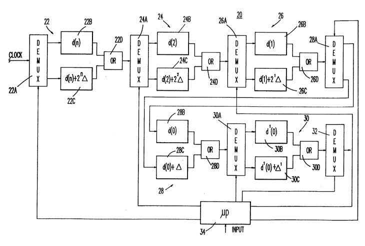
Referring now to FIG. 1, a circuit 20 is shown for
imposing a selectable, highly accurate time delay,
relative to a circuit path of minimum delay, on a
digital/pulse electronic input signal. This time delay
is referred to herein as a "differential delay".
Circuit 20 includes five series-connected delay
stages 22, 24, 26, 28, 30, each stage including a
demultiplexer (DEMUX) 22A-30A, a first circuit path
22B-30B of minimum time delay, a second circuit path
22C-30C of minimum delay plus an additional delay, and a
logical OR gate 22D-30D. As described below, the "C"
circuit paths 22C-30C are connected in parallel with their
corresponding "B" circuit paths 22B-30B between bracketing
pairs of DEMlJXs and OR gates.
DEMUX 22A is connected to receive a digital clock
input signal CLOCK and to steer that signal to a selected
one of circuit paths 22B or 22C. Logical OR gate 22D is
selected to receive the outputs from both of circuit paths
22B, 22C. DEMUX 24A is connected to receive the output
FI9-87-010 6
ZO(~7413
-
of OR gate 22D, and to steer the output of the OR gate to
a selected one of circuit paths 24B or 24C. DEMUXs 26A,
28A, and 30A are likewise connected to receive the output
of the OR gate from the previous stage, and to steer the
signal to a selected one of the circuit paths in the
subsequent stage.
An output DEMUX 32 is connected to receive and drive
the output signal from OR gate 30D. A microprocessor 34
has an input connected to receive data from at least two
period counters (FIGs. 3, 5), and outputs connected to
each of DEMUXs 22A-30A and 32 for controlling the DEMUXs
in a manner described below.
Examining now FIG. 2, one embodiment of delay stage
22 is shown wherein DEMUX 22A comprises four logical OR
gates 36, 38, 40, 42. Gate 36 has an input connected to
receive clock signal CLOCK, and an inverting output
connected to a first input for each of gates 40, 42. Gate
38 has an input connected to receive a control signal Cl
from microprocessor 34, an inverting output connected to
the second input of gate 40, and a non-inverting output
connected to the second input of gate 42.
Circuit path 22B comprises a single logical OR gate
44 having its input connected to an inverting output of
gate 40, and an output connected to an input of gate 22D.
Circuit path 22C comprises X series-connected logical OR
gates 46-46X, the first gate having its input connected
to an inverting output of gate 42. The output of gate 46X
is connected in parallel to one input of Y
FI9-87-010 7
parallel-connected gates 48-48Y, and to the second input
of gate 22D.
It will be understood that subsequent delay stages
24-30 of delay circuit 20 are constructed similarly to the
embodiment of delay stage 22 shown and described in FIG.
2, the only difference being the number of series and
parallel connected gates, X and Y, respectively, in the
"C" delay paths. In a manner described in further detail
below, the arrangements of gates in each of the "C"
circuit paths is selected to provide a desired signal
delay.
In operation, described particularly with respect to
the notation used in the "B" and "C" delay paths of stage
22, delay path 22B is constructed so as to provide a
typical time delay d(n). Delay path 22C i~ constructed
to provide a time delay approximately equal to the delay
d(n) of signal path 22B, plus an additional delay of 2h x
delta (delta2~) where: delta equals a minimum, physically
realizable delay increment, and n is a power of 2 selected
dependant on a desired maximum delay, and generally
determinative of the number of delay stages in circuit 20
(not including multiple minimum, 2 delay stages such as
stages 28, 30).
In the preferred embodiment of the invention shown,
each "C" delay path 22C-28C of delay circuit 20 includes
an additional delay, relative to its corresponding "B"
circuit path, equal to a power of 2 times the delta delay,
and the various "C" delay paths are arranged relative to
FI9-87-010 8
1 3
one-another in ascending/descending binary order.
Assuming, for purposes of describing the present invention
that n=3, circuit 20 thus includes 4 stages: n~3 (stage
22), n=2 (stage 24), n=l (stage 26), n=O (stage 28), and
one extra n=O stage (stage 30) for purposes of increasing
delay accuracy in a manner described below. The resulting
additional "C" delay path is what is commonly referred to
in the art as a binary ladder.
Examining the delays in each of the stages, delay
path 22C includes a delay of 23 x delta (delta23) relative
to path 22B. Delay path 24C includes a delta2~ delay
relative to path 24B. Likewise, delay paths 26C, 28C, and
30C include delta delays of delta2 , delta2 , and delta'2
, relative to their corresponding "B" delay paths. In a
manner described in further detail below, the additional
delay~ in the "C" circuit paths (relative to their
corresponding "B" circuit paths), are provided through the
appropriate selection of gates in the "B" and "C" circuit
paths (i.e. the numbers X, Y of series, parallel connected
gates).
For purposes of describing the present invention, it
will be assumed that a logical OR gate such as gate 44 or
46, when driving a single output load, exhibits a typical
delay time of about 160 picoseconds (ps). Each
series-connected gate, such as gate 46, thus increases the
signal delay time through a circuit path "C" by
approximately 160 ps, allowing large values of delay to
be obtained. To obtain smaller values of delays, a
FI9-87-010 9
2~07~:~3
parallel-connected gate, such as gate 48, will be provided
and assumed to increase the signal delay time through the
circuit path by approximately 20 ps.
It will be understood that the gate delay time is a
function of the fabrication of a gate, and may vary
considerably from the 160 ps (series) and 20 ps (parallel)
examples selected for purposes of explaining the operation
of the present invention.
Further, it is a fundamental consideration of the
present invention that, due to uncontrollable variations
in logic gate fabrication and interconnection, no given
logic gate is likely to exhibit the exact, typical delay
- assumed here to be 160 ps for a series- and 20 ps for a
parallel-connected gate. It is well known in the art that
variations in external conditions, particularly ambient
temperature and supply voltage levels, will also cause the
gate delays to vary in a proportional manner.
Continuing to describe the operation of the present
invention, the assumption is continued that circuit 20 is
constructed to have n=4 delay stages 22, 24, 26, 28, and
an extra, minimum 2 delay stage 30. It will further be
assumed that it is desired to realize a minimum delta
delay of 20 ps. From a consideration of the above
discussion of gate delay times, it will be apparent that
a minimum delta delay of 160 ps is realizable with a
single, series-connected gate, or multiple,
parallel-connected gates.
FI9-87-010 10
~o~
Pursuant to the above-described parameters, "B"
circuit paths 22B-30B are selected to exhibit typical
delays of d(3)=d(2)=d(1)=d(0)=d'(0)=160 ps
(approximately). These delays are set by the selection
of the number and connection of gates in each of the "B"
delay paths. Delay path 22C has the gates therein
connected to provide a delay of 160 ps + 23 x 20 ps = 320
ps. Circuit path 24C is constructed to exhibit a time
delay of 160ps + 2~ x 20ps = 240ps, and circuit path 26C
a delay of 160ps + 21 x 20ps = 200ps. Likewise, circuit
paths 28C and 30C are each constructed to provide a
minimal delay: 160ps + 2 x 20ps = 180ps.
Because of the variations in individual gate delays
as described above, it will be understood that the various
delay paths cannot be constructed to have the exact
desired delays. However, through a combination of
theoretical calculation and, where practical, actual
measurements, the various "B" and "C" delay paths are
fabricated to be as close to the desired delays as is
practicable.
Subtracting the typical "B" stage delay of d(n)=160
ps from each "C" delay stage, Table 1 below sets out the
theoretical additional delay available through each of
circuit paths 22C-30C.
FI9-87-010 11
20074~3
TABLE 1
Circuit Path Theoretical Additional Delay
22C 23 x 20ps = 160ps
24C 2d x 20ps = 80ps
26C 2I x 20ps = 40ps
28C 2 x 20ps = 20ps
30C 2 x 20p~ = 20ps
320ps = max.
additional delay
From a consideration of the above, it will be
understood that, through appropriate control of the DEMUXs
22A-30A by micro-processor 34 in accordance with a method
described below, delay circuit 20 is capable of generating
a pulse having a selected additional delay of between 20
ps and 320 ps, in binary 20 ps (minimum delta delay)
increments. This selected, or differential delay is
relative to a minimally delayed pulse propagated
exclusively through circuit paths "B".
However, while circuit 20 provides for a differential
time delay in very fine increments of about 20ps, for the
reasons described above, no particular gate in circuit 20
can be expected to exhibit the exact, theoretical delay.
Each delta delay path 22C-30C will thus vary to some
extent from the theoretical delay set out in Table 1.
A method and apparatus for more exactly calibrating
the time delays selectable with delay circuit 20 will now
be described with respect to FIGs. 3 and 4.
Referring first to FIG. 3, a calibration circuit 60
is shown for calibrating the operation of delay circuit
so that actual additional delays can be measured
~I9-87-010 12
Z~i7~13
._
through each circuit path 22C-30C. Calibration circuit
60 includes a logical OR gate 62 having a first input
connected to receive clock signal CLOCK, and an output
connected to the input of delay circuit 20. The output
of delay circuit 20 is connected both to an optional
coarse delay circuit 64 and to the first input of a
logical OR gate 66. The output of coarse delay circuit
64 is provided for subsequent use by a system (not shown)
requiring much larger delays that are multiples of the
input clock of the present invention. For example, an
integrated circuit testing system.
Gate 66 has a second input for receiving a
calibration enable signal CAL ENABLE, a noninverting
output connected to a period counter 68, and an inverting
output connected back to the second input of gate 62. A
feedback loop is thus formed between the input and output
of delay circuit 20 via gates 66 and 62.
Coarse delay circuit 64 comprises a circuit, many
configurations of which are known to those skilled in the
art, for adding a coarse time delay to the relatively fine
time delay provided by delay circuit 20. Period counter
68 comprises a conventional period counter, preferably
accurate to about one one-hundreth of the delta time delay
selected in signal path "C" of delay circuit 20. One such
period counter comprises the Hewlett Packard model HP5385A
frequency counter, accurate to approximately 0.0l ps.
In operation, the calibration enable signal CAL
ENABLE is selected to enable gate 66 whenever it is
FI9-87-010 13
20~7413
desired to measure the actual (vs. the theoretical, or
typical) time delays through the signal paths of delay
circuit 20: i.e. to measure both the total minimum delay
through the "B" signal paths and the delay (including the
additional delay) through each of the "C" signal paths.
Such calibration may be performed, for example, on first
applying power to delay circuit 20, and periodically
thereafter during the operation of the circuit.
With gate 66 and period counter 68 both enabled, the
period counter will accurately count the time period
between adjacent digital pulses provided thereto.
Microprocessor 34 is first operated to control DEMUXs
22A-30A so as to select the minimum time delay path, i.e.
the "B" signal path in each of stages 22-30. Period
counter 68 thus measures the actual minimal delay through
delay circuit 20. After this minimal delay is known,
microprocessor 34 is operated to control the same DEMUXs
so as to select, one at a time, the relatively delayed,
or "C" signal paths, through delay circuit 20, while the
remaining DEMUXs select a "B" signal path. Thus, as each
"C" signal path is selected, its actual additional delay
relative to the minimum signal delay is straightforwardly
determined by subtracting the delay with the selected "C"
signal path switched in from the minimum delay "B" signal
path. This calculation is preferably performed in
microprocessor 34. When each of the "C" signal paths
22C-30C has been selected in turn, the actual additional
delay through each of these circuit paths is known.
FI9-87-010 14
~0~7413
Table 2, set out below, includes a set of exemplary,
actual/measured additional delays for the circuit paths
22C-30C. Such actual delays are obtained using the
calibration circuit of FIG. 3 in the manner described
immediately above.
TABLE 2
Theoretical Actual
Delay StageAdd. Delay Add. Delay
22C 160ps 152.5ps
24C 80ps 85.8ps
26C 40ps 36.3ps
28C 20ps 17.2ps
30C 20ps 16.7ps
Referring now to FIG. 4A, a method is provided for
using the actual additional delays measured in circuit
paths 22C-30C to determine the signal path through delay
stages 22-30 which will provide a differential delay
closest to a desired delay DD. The method will be
described first in general, and then in an example with
circuit 20 having the theoretical and actual delta delays
set out in Table 2 above.
In general, the method and apparatus of the present
invention permit the selection of a desired delay based
on the theoretically possible delays (i.e. a power of 2
times the delta delay). However, because the actual
delays measured through the various signal stages differ
from the theoretical delays, a differential delay is
generated, based on the actual delays, which has the
smallest possible error relative to the desired delay.
Generally, starting with the largest additional delay
stage and continuing in descending order, each actual
FI9-87-010 15
2007~13
delay is added to a previously selected total delay. If
the selection of that actual delay provides a differential
delay having a smaller error relative to the desired
delay, then a record is made and that delay stage is
selected for use in generating the differential delay.
If the selection of that actual delay results in a
differential delay having a larger error relative to the
desired delay, then the actual delay is not selected.
When all of the actual delays have been utilized as
described above, the selected, actual, differential delay
will provide the smallest possible error relative to the
theoretical desired delay.
The method assumes the availability of a bit storage
array B(N) having a flag bit for each of the n+l delay
stages in circuit 20 (i.e. a lx5 array). The error
between the desired delay DD and the calculated delay at
any given time during the execution of the method is
indicated by ERR. The method is typically executed as a
computer program in microprocessor 34.
The following Table 3 defines the variables used in
the subject method. Those variables indicating they may
be measured in seconds are, of course, measures of time.
TABLE 3
DD - desired delay (seconds)
B(n) ~ bit flag for an n-long array `
BF - bit flag counter
ERR - delay error (sec.)
MIN ERR - minimum error (sec.)
POS ERR - positive error (sec.)
N - cycle counter
deltaa - actual, additional delay at the 2n "C"circuit path
FI9-87-010 16
~74~.3
-
The method is initiated by setting a cycle counter N
equal to the number of delay stages in the delay line
circuit minus l, and the minimum error MIN ERR to the
actual additional delay delta2~ of the largest delay
stage.
The desired delay DD is entered, and positive error
POS ERR is set equal to the desired delay DD. The
additional delay delta2~ is subtracted from the positive
error POS ERR to calculate error ERR.
The error delay ERR is checked to determine if it is
greater than or less than 0. The "greater than O"
operations will be described first.
Assuming that the error delay ERR is greater than 0,
the bit flag associated with the n delay stage B(N) is set
equal to one, indicating that that additional delay (i.e.
that "C" signal path) will be used, and the positive error
POS ERR is set equal to the error ERR.
The error ERR is checked to determine if it is less
than the minimum error MIN ERR. If error ERR is less than
minimum error MIN ERR, then MIN ERR is set equal to ERR,
and bit flag counter BF is set equal to -1, indicating the
minimum error occurred when error ERR was positive. If
error ERR is greater than minimum error MIN ERR, than the
above steps are not performed. Next, N is checked to see
if it is zero. If N is not equal to zero, then N is
decremented and the loop is repeated.
Describing now the operation when the error delay ERR
is less than zero, the addition of more additional delays
FI9-87-01~ 17
~~ 3
would result in a more negative delay error ERR.
Therefor, the bit flag B(N) is set to zero so as not to
select the present additional delay (i.e. not to select
the present "C" delay stage). The magnitude of the delay
error ¢ERR! is checked to see if it is less than the
minimum error MIN ERR. If it is, then the minimum error
MIN ERR is set to the magnitude of the delay error ERR,
and the bit flag counter BF is set to N to indicate that
the minimum error MIN ERR occurred for a negative delay
error ERR, and to indicate at which additional delay stage
n it occurred. If the magnitude of the delay error ¢ERR'
is not less than the minimum error MIN ERR, then the above
steps are not performed. Next, N is checked to see if it
is equal to zero. If N is not equal to zero, then N is
decremented and the loop is repeated.
The above-described process is repeated for as long
as N is not equal to (i.e. N is greater than) zero. When
N=O, the bit flags B(N) identify the "C" signal paths
which give the smallest positive minimum error relative
to the desired delay. However, it is also possible that
the minimum error occurred for a negative delay error.
Referring now to FIG. 4B, the bit flag counter BF is
checked to see if it equals -1. If it does, it indicates
that the minimum error occurred for a positive delay error
and the bit flags B(N) identify the "C" signal paths which
will provide the best differential delay. The program is
thus ended.
FI9-87-010 18
Z(~ 13
If the bit flag counter BF is not equal to -1, it
indicates that the minimum error occurred for a negative
delay error, and that it occurred during the loop cycle
when N=BF. Therefor, all delays that were selected when
N>BF stay selected. Delay (BF) is also selected by
setting B(BF) equal to 1. The additional delays for which
N<BF are all deselected. These last steps are shown in
the lower loop in FIG. 4B. After B(BF) is set to 1, the
bit flag counter BF is decremented and checked to see if
it is equal to -1. If it is not, then B(BF) is set to zero
(i.e. that "C" stage additional delay is deselected) and
the lower loop is repeated. The program is ended when the
bit flag counter BF is found equal to -1.
Upon the completion of the process shown in FIGs.
4A, 4B, the optimal path through delay circuit 20 (FIG.
1) is chosen, the "C" circuit path being selected for each
delay stage wherein the bit flag array B(N) = 1. As will
be appreciated from a consideration of the example below,
the above-described method provides a differential delay,
based on the actual measured delta delay for each "C"
circuit path, which is closest to the desired delay DD.
As will also be appreciated, the circuit path thusly
calculated may differ from that which would be calculated
based on theoretical delta delays.
The above-described process will now be illustrated
with respect to two separate examples: the first example
having a desired delay DD of 240ps, and the second example
having a desired delay DD of lOOps.
FI9-87-010 19
20~7~3
Example 1
The values obtained in performing the above-described
process for a desired delay DD of 240ps are set out in
summary form in Table 4 below. The process is started by
initiating cycle counter N equal to the number of stages
in circuit 20 minus 1: N = 5 - 1 = 4. The minimum error
MIN ERR is set equal to the highest order actual delay:
MIN ERR = delta23 = 152.5ps (all actual delays are
obtained from Table 2 above).
With N=4, positive error POS ERR is set equal to
desired delay DD: POS ERR = 240ps. The actual delay
delta2n is subtracted from positive error POS ERR to
obtain error ERR: ERR = 240 - 152.5 = 87.5ps. Because
error ERR is greater than 0, bit flag B(4) is set to 1,
and positive error POS ERR is set equal to ERR: POS ERR =
87.5ps. Because error ERR is less than minimum error MIN
ERR (87.5 < 152.5), MIN ERR is set equal to ERR: MIN ERR
= 87.5ps, and bit flag counter BF is set equal to -1.
With N decremented so that N = 3, ERR = POS ERR -
delta2 f ERR = 87.5 - 85.8 = 1.7. Because ERR is greater
than 0, B(3) is set to 1, and POS ERR = ERR = 1.7. Because
ERR < MIN ERR (i.e. 1.7 < 87.5), then MIN ERR is set equal
to ERR, and bit flag counter BF is set equal to -1: MIN
ERR = 1.7, BF = -1.
With N decremented to N = 2, ERR = POS ERR - delta2
: ERR = 1.7 - 36.3 = -34.6. Because ERR is less than 0,
B(2) ia set to 0. Because abs(ERR) is not less than MIN
FI9-87-010 20
ERR (i.e. abs(-34.6) is not less than 1.7), N is
decremented and the loop is repeated. POS ERR, MIN ERR,
and BF remain unchanged.
With N decremented to N = 1, ERR = POS ERR - delta2
ERR = 1.7 - 17.2 = -15.5. Because ERR is less than 0,
B(2) is set to 0. Because abs(ERR) is not less than MIN
ERR (i.e. abs(-15.5) is not less than 1.7), N is
decremented and the loop is repeated. POS ERR, MIN ERR,
and BF remain unchanged.
With N decremented to 0, ERR = POS ERR - delta2':
ERR = 1.7 - 16.7 = -15. Because ERR is less than 0, B(l)
is set equal to 0. Because abs(ERR) is not less than MIN
ERR (i.e. abs(-15) is not less than 1.7), N is decremented
and the loop is repeated. POS ERR, MIN ERR, and BF remain
unchanged.
TABLE 4
POSS ERR< MIN
N ERR B(n) ERR MIN ERR? ERR BF
4 87.5 1 87.5 Y 87.5 -1
3 1.7 1 1.7 Y 1.7 -1
2 -34.6 0 1.7 N 1.7 -1
-15.5 0 1.7 N 1.7 -1
0 -15.0 0 1.7 N 1.7 -1
Because N is now decremented to 0, the process
continues as shown in FIG. 4B. Because bit flag counter
BF is equal to -1, the process is ended.
Examining the contents of bit flag array B(n) and
relating those contents to circuit 20 of FIG. 1, it is
seen that "C" circuit paths have been selected for the
highest order (i.e. delay stage 22) and the second-highest
FI9-87-010 21
~0074~3
order (i.e. delay stage 24) stages of circuit 20. In
fact, selecting those "C" circuit paths will yield a
differential delay time of 238.3ps (152.5 + 85.8) relative
to the minimal delay through the "B" circuit paths.
Example 2
In this example, the desired delay is selected to be
lOOps. N is again initialized to 4, and MIN ERR to 152.5.
Because the steps shown in FIG. 4A are performed
analogously to those of example 1 above, the results are
presented in summary form in Table 5, below.
TABLE 5
POSS ERR< MIN
N ERR B(n) ERR MIN ERR? ERR BF
4 -52.5 0 100.0 Y 52.5 4
3 14.2 l 14.2 Y 14.2 -1
2 -22.1 0 14.2 N 14.2 2
l -3.0 0 14.2 Y 3.0
0 -2.5 l 14.2 Y 2.5 0
Analyzing the results of Table 5 with respect to the
process of FIG. 4B, it is seen that when bit flag counter
BF is checked the first time it is not equal to -l, but
to 0. Therefor, continuing the process as shown in the
Fig.4B, B(BF) = B(0) is set equal to 1. The bit flag
counter BF is decremented from 0 to -1, and the process
is ended.
Examining the contents of the bit flag array B(N),
it is seen that the flags are set to l for both the second
from the highest order delay, and for the primed lowest
FI9-87-010 22
20074i3
_,
order delay. The indicated "C" paths through circuit 20
of FIG. 1 are hence the delta2~ "C" path of 85.8ps plus
the delta2D' "C" path of 16.7ps for a total differential
delay of 102.5ps. The reader can straightforwardly
convince himself that this is the optimum signal path to
obtain the desired lOOps delay. The only other path which
is close would substitute the first lower order delay of
17.2ps for the identified 16.7ps path, increasing the time
away from the desired lOOps.
The inclusion of the multiple lower order delays, in
this case the two lower order stages 28C and 30C of delay
circuit 20, has been discovered by the present inventors
to substantially increase the accuracy with which the
desired delay can be generated. In fact, assuming that
the actual, measured delay of each delay stage varies
randomly about the theoretically expected delay, the
inclusion of two or more lowest order delay stages will
have an unexpectedly dramatic and substantial affect in
reducing the error with which a sub-nanosecond delay in
the above-described range can be generated.
Referring now to FIG. 5, a loop oscillator circuit
70 is shown situated on a portion of an integrated circuit
chip 72 which also supports delay circuit 20 and
calibration circuit 60. Loop oscillator circuit 70
comprises, for example, an arrangement of series-connected
logic gates with a feedback path and a connection to a
period counter 74.
FI9-87-010 23
200~4~3
~
In operation, the period of loop oscillator circuit
70 is measured with period counter 74 during the initial
start-up of the logic on integrated circuit chip 72. This
measuring of the loop - oscillator frequency is performed
substantially simultaneously with the initial calibration
of delay circuit 20 as described above. The frequency of
loop circuit 70 is then periodically monitored as chip
portion 72 continues to operate, generating heat and
eventually reaching full operating temperature. Because
loop circuit 70 is positioned adjacent, and likely
intertwined to some extent with delay circuit 20, changes
in signal periods which are exhibited by loop circuit 70
can be presumed to be substantially identical to similar
changes exhibited in delay circuit 20. A scaling factor
is thus readily determined to scale any changes in gate
delay times back to the gate delays measured at start-up
(or at the first calibrating measurement).
In accordance with the present invention, the scaling
factors determined by monitoring the frequency of loop
oscillator circuit 70 are used to scale the delta delays
measured through the various stages of delay circuit 20
during the calibration process described above. This
scaling of the delta delays in delay circuit 20 is
preferably performed in microprocessor 34, and requires
substantially less time to perform than a complete
recalibration of the type described above.
FI9-87-010 24
2007~13
Table 6 below illustrates the scaling of the measured
delta delays with a scaling factor, A, selected to
compensate for a change in gate delays.
TABLE 6
Measured Delta Delays Scaled Delta Delays
delta2' A x delta2'
delta2 A x delta2
delta21 A x delta2
....... ...... ....
delta2n A x deita2~
From a consideration of Table 6, it is seen that the
scaling factor is applied easily and quickly by simple
linear multiplication of the measured additional delays.
There has thus been provided a delay circuit which
is programmable to generate selectable time delays in the
subnanosecond range. In the embodiment shown, the minimum
delay is determined by the propagation delay of a digital
gate, and the delay is variable in binary increments. It
will be understood, however, that the invention is not so
limited. The delays may alternately be provided by other
signal delaying means, such as conventional delay lines,
and needn't be provided in a binary ladder format.
In accordance with the present invention, the
generated delays are based on the actual, measured delay
paths through the circuit, versus the theoretically
calculated delays. The present invention thus provides a
system for generating highly accurate, very fine delays
in programmable increments. Methods and apparatus for
calibrating the delay circuit and for selecting
appropriate delay paths based on measured delay values are
FI9-87-010 25
2007413
provided. Further provided is a method and apparatus for
scaling the measured delays based on changes caused, for
example, by thermal or supply voltage fluctuations. The
subject invention has particular application in
semiconductor chip testers, wherein selectable, highly
accurate time delays are required in great quantity.
While the present invention has been described with
respect to a particular embodiment, it will be understood
by those skilled in the art that various changes and
improvements may be made without departing from the spirit
and scope of the present invention.
FI9-87-010 26