Note: Descriptions are shown in the official language in which they were submitted.
TITLE OF THE INVENTION
Magnetic Head
CROSS-REFERENCE TO RELATED COPENDING APPLICATION
The present application is related to a copending US
application serial No. 218,018 filed on July 12, 1988,
owned by the same assignee.
BACKGROUND OF THE INVENTION
Field of the Invention
The present invention relates to a magnetic head and,
more specifically, to a magnetic head used in a magnetic
recording and reproducing apparatus such as a video tape
recorder (VTR) or a digital audio tape recorder (DAT).
Description of the Background Art
In recent years, there has been an increasing
tendency to higher density of recorded signals in a
magnetic recording and reproducing apparatus such as a VTR
or a VAT. Metal tapes of high coersive force formed by
using ferromagnetic metal powder such as Fe, Co or Ni as
magnetic powder have been used for such high~density
recording. For example, metal tapes haying a high
coersive force, Hc = about 1400 to 1500 oersteds are used
for small-sized VT}~s known as 8mm video tape recorders.
This is because a recording medium making it possible to
shorten wavelength of recorded signals is required for the
.
2~
necessity of increasing recording density to reduce the
size of the magnetic recording and reproducing apparatus.
Meanwhile, if a conventional magnetic head made only
of ferrite is used for recording on the metal tape, a
magnetic saturation phenomenon occurs, because a
saturation flux density of ferrite is only 5500 gauss at
most, and accordingly, optimum performance of the metal
tape cannot be achieved. A magnetic head adapted for a
metal tape having a high coersive force needs to have a
high saturation flux density in the vicinity of a gap of a
magnetic core, other than high-frequency characteristics
and abrasi.on resistance of the magnetic core as generally
required for magnetic heads. In order to satisfy such
requirements, it is proposed Jo use, as a magnetic head
lS adapted for a metal tape, a magnetic head made of a
metallic magnetic material such as permalloy, sendust or
amorphous magnetic material having a large saturation
magnetization than that of ferrite used for a magnetic
core (such a magnetic head being hereinafter referred to
as a composite type magnetic head or MIG (Netal In Gap)).
Such a composite type magnetic head has excellent
characteristics in reliability, magnetic properties,
abrasion resistance and the like.
Fig. 1 is a perspective view showing an appearance of
a conventional magnetic head. As shown in Fig. 1, a pair
-- 2 --
.. . . . .
2~t~76~
of magnetic core halves la and lb made of a ferromagnetic
: oxide such as ~n-Zn ferrite are opposed to each other
through a non-magnetic material with a magnetic gap 2
being provided therebetween, and thin films of a magnetic
material such as sendust are formed near the magnetic gap
2. The magnetic core halves la and lb are joined by glass
4 with a coil groove 5 being provided.
In the composite type magnetic head thus provided,
the thin films 3 of the ferromagnetic metal are deposited
by sputtering on upper surface areas of the base of the
ferromagnetic oxide where mirror surface finishing has
been applied. However, junction regions between the thin
films of the ferromagnetic metal and the base of the
ferromagnetic oxide are non-magnetized due to
interdiffusion and chemical reactions of constituent
elements, or irregular arrangement in crystal structure.
As a result, those regions function as pseudo gaps,
exerting adverse effect on the performance of the magnetic
head.
More specifically, as shown in Fig. 1, pseudo gaps
are formed on boundary faces 6 between the magnetic core
halves la and lb and the thin films 3 of the ferromagnetic
metal, respectively, other than the prescribed magnetic
gap 2. If a singly reverse-magnetized recorded signal on
a magnetic tape is reproduced by using the magnetic head
~i3~ 8
having boundary faces where such pseudo gaps are formed as
shown in fig. 3, pseudo signals 8a and 8b are reproduced
with deviations of time = t/v before and after
reproduction of the prescribed signal. 7. In the equation,
t represents a thickness of each of the ferromagnetic
metal thin film 3 in the relative travelling direction
defined between the head and the tape, and v represents a
relative ~ravelling speed defined between the head and the
tape.
On the other hand, if continuously reverse-magnetized
recorded signals having a recorded wavelength
substantially equal to or shorter than t are reproduced,
the pseudo signals 8a and 8b as shown in Fig. 3 can not be
readily observed. However, if the frequency
characteristics of the reproduced output are measured, a
frequency characteristic curve which waves with peaks at
frequency satisfying f = n-(v/t) and bottoms at a
frequency satisfying f = (n-l/2)-(v/t), where f indicates
frequency Y and n indicates a natural number, is
obtained as shown in Fig. 4 by superposition of the
reproduced output through the pseudo gaps onto the
reproduced output ~hrouqh the pr~scribed-magnetic gap 2.
Accordingly, if a magnetic head having boundary faces 6
where such pseudo gaps are formed is used for a VTR or
DAT, pseudo signals due Jo the pseudo gaps cause noises,
2~
resulting in a deterioration of the quality of the picture
or adverse effects on the performance of the magnetic
head, such as increase of an error rate. Particularly, in
the case of using a magnetic head having a magnetic gap 2
parallel to the boundary faces 6 where such pseudo gaps as
shown in Fig. 1 are generated, a ~Javing phenomenon in the
frequency characteristics of the reproduced output is
observed and the S/N ratio is deteriorated.
In order to suppress generation of such pseudo gaps,
it is proposed to adapt a method for applying reverse
sputtering to a surface of a base member of a
ferromagnetic oxide such as ferrite under suitable power
supply conditions immediately before formation of the thin
films of ferromagnetic metal, as disclosed, for example,
in Japanese Patent Laying Open No. 62-57115. However,
even this method can not completely remove portions
adversely affected by the treating process of the thin
film which would cause the pseudo gaps, and accordingly
this method is not sufficiently effective for preventing
generation of pseudo gaps.
Further, as shown in Fig. 2, a composite type
magnetic head is proposed in which boundary faces 6
between magnetic core halves la and lb and thin films 3 of
ferromagnetic metal, respectively have an inclination and
: 25 are not parallel to the faces forming the magnetic gap 2,
.. .. . ..
~C~7~
causing no adverse effect to the perEormance of the head
even if the pseudo gaps are generated. However, the
magnetic head having such structure is not suited for mass
production because the manufacturing process thereof is
complicated and the manufacturing cost comes to be high
compared with the magnetic head having the boundary faces
6 parallel to the magnetic gap 2 a shown in Fig. 1.
The inventors of the present invention have been
interested in the following three points as causes of
pseudo gap generation of the magnetic head having the
parallel type MIX (Metal In Gap) structure shown in Fig.
1.
(i) deterioration of crystallinity of the surface of
the base formed of ferromagnetic oxide such as ferrite.
(ii) turning into amorphous of the initial layer of
the ferromagnetic thin film formed of ferromagnetic metal
material such as sendust.
(iii) diffusion or chemical reaction at the junction
region between the thin films of ferromagnetic metal and
the base formed of ferromagnetic oxide.
The inventors of the present invention have invented
and disclosed a magnetic head capable of preventing the
above described causes (i) and (iii) of the pseudo gap
generation and manufacturing method thereof in Japanese
Patent Laying-Open No. 62-175157 filed on July 14, 1987,
-- 5 --
... . . . .
l8
Japanese Patent Laying-Open No. 62-134893 filed on August
4, 1987 and in USSN 218,018 claiming priorities based on
the above mentioned Japanese application.
SUMMARY OF THE INVENTION
An object of the present invention is to provide a
magnetic head which makes it possible to effectively
suppress generation of pseudo gaps in junction regions
between magnetic core halves and thin films of
ferromagnetic metal, or to effectively prevent t.he
junction regions from exerting adverse effect as a result
of function as pseudo gaps.
The magnetic head in accordance with the present
invention has a pair of magnetic core halves opposed to
each other with a non-magnetic material interposed
therebetween to form a magnetic gap, which comprises a
pair of magnetic core halves, interposed thin films and
ferromagnetic thin films. $he pair of magnetic core
halves are formed of ferromagnetic oxide and have gap
forming faces to be opposed to each other for forming the
magnetic gap. The interposed thin films are formed on the
gap forming faces and formed of minute crystal grains.
The ferromagnetic thin films are formed of ferromagnetic
metal material on the interposed thin films. The
f rromagnetic thin films are thin films having crystal
.
8~
grains grown immediately on the surface of the interposed
thin films.
In a preferred embodiment of the magnetic head of the
present invention, the ferromagnetic thin film is a
polycrystalline substance including crystal grains having
at least one of ~110} face, ~200~ face and {211} face as a
face approximately parallel to the gap forming face. More
preferably, the ferromagnetic thin film i5 a
polycrystalline substance including crystal grains having
{110} face, crystal grains having ~200} face and crystal
grains having ~211} race as the faces approximately
parallel to the zap forming ace. Preferably, the
thickness of the interposed thin film is not less than lnm
and not more than 1/10 of the thickness of the magnetic
gap. The minute crystal grains may be former of
non-magnetic oxide such as silicon oxide. The
ferromagnetic metal material may include sendust, and the
ferromagnetic oxide forming the magnetic core halves may
; include ferrite.
When a ferromagnetic thin film is formed on the gap
forming face forrned of fexromagnetic oxide, the initial
layer of film formation may possibly be a deteriorated
magnetic layer hazing irregular atomic arrangement, due to
the irregular arrangement of the cxystal structure with
the underlying face. In the magnetic head of the present
I'
-- 8 --
;i 8~
invention, a thin film formed of minute crystal grains is
interposed between each of the magnetic core halves formed
of ferromagnetic oxide and the ferrornagnetic thin film.
The thin film formed of minute crystal grains has the
effect of intercepting adverse effect of the atomic
arrangement of the surface of the magnetic core halves
formed of ferromagnetic oxide on the formation of the
initial layer of the ferromagnetic metal thin films.
Consequently, the ferromagnetic metal thin film formed on
the thin film of minute crystal grains grows as a film
having inherent crystal structure from the very beginning
: of formation thereof. Accordingly, the deteriorated
magnetic layer having irregular atomic arrangement is not
formed in the initial layer of the ferromagnetic thin
film, and the cause of pseudo gap generation can be
removed. Consequently, deterioration of the reproduced
output from the magnetic head caused by the pseudo gaps
can be suppressed.
Namely, according to the present invention, the
initial layer of the thin film formed of ferromagnetic
: metal can be prevented from being turned into amorphous,
which was the cause of pseudo gap generation, by forming
thin films of minute crystal grain on the gap foxming
faces formed of ferromagnetic oxide.
_ g _
:
2~(376~8
The foregoing and other objects, features, aspects
and advantages of the present inventi.on will become more
apparent from the following detailed description of the
present invention when taken in conjunction with the
accompanying drawings.
BRIEF DESCRIPTION OF THE DRAWINGS
Figs. 1 and 2 are perspective views showing
- appearances of conventional magnetic heads;
Fig. 3 is a diagram showing a reproduced signal
through a magnetic gap and reproduced signals through
pseudo zaps;
Fig. 4 is a graph showing frequency characteristics
of an output by a conventional magnetic head;
Fig. 5 is a perspective view showing an appearance of
the magnetic head of the present invenkion;
Fig. 6 is a plan view showing a tape contact face of
the magnetic head shown in Fig. 5;
Fig. 7 is a schematic diagram showing a sputtering
apparatus used for sputtering in film formation or for
reverse sputtering, in manufacturing the magnetic head of
the present invention;
Figs. 8A, 8B, 9A, 9B, 10A, 10B and ll are perspective
views specifically showinq steps of manufacturing the
magnetic head in accordance with one embodiment of the
present invention;
-- 10 --
~3~
Fig. 12 shows X-ray diffraction patterns Qf the
ferromagnetic metal thin films of respective film
thicknesses formed with the thin film of minute crystal
grain interposed;
Fig. 13 shows a X-ray diffraction pattern of the
ferromagnetic metal thin films of respective film
thicknesses without the thin film of minute crystal grains
interposed, for comparison with the present invent:ion;
Fig. 14 schematically shows crystal structure of the
ferromagnetic metal thin film formed with the thin film of
minute crystal gL^ains interposed, in accordance with the
present invention;
Fig. 15 schematically shows crystal structure of the
ferromagnetic thin film formed without the thin film of
minute crystal grains interposed, for comparison with the
present invention;
Fig. 16 shows frequency characteristics of the
reproduced output measured through the magnetic head
having the ferromagnetic metal thin film formed with the
thin film of minute crystal grains interposed, in
accordance with the present invention;
Fig. 17 shows frequency characteristics of the
reproduced output measured through the magnetic head
having the ferromagnetic metal thin film formed without
.,
7~
the thin film of minute crystal grains interposed, for
; comparison with the present invention;
Fig. 18 shows a result of measurement of the surface
roughness of the ferrite baseJ with the ferromagnetic
metal thin film, which is formed with the thin fi]m of
minute crystal grains interposed in accordance with the
present invention, being removed by ion beam etching; and
Fig. l9 shows a result of measurement of the surface
roughness of the ferrite base, with the ferromagnetic
metal thin film, which is formed without the thin film of
minute crystal grains interposed, being removed by ion
beam etching, for comparison with the present invention.
DESCRIPTION OF THE PREFERRED EMBODIMENTS
One embodiment of the present invention will be
described in detail with reference to the figures.
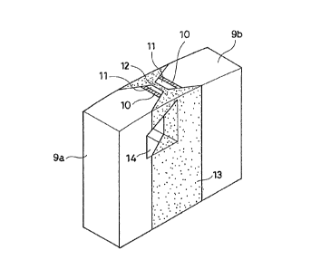
Referring to Fig. 5, thin films 10 of minute crystal
grains are formed on the gap forming faces of the magnetic
core halves 9a and 9b formed of ferromagnetic oxide such
as Mn-Zn single crystal or polycrystalline ferrite, Ni-Zn
single crystal or polycrystalline ferrite, or ferxoxplana.
The thin films 10 of minute crystal grains are thin films
having minute crystal grains nearly with the nature of
amorphous, formed Jo have the thickness of about several
nm to several 10 nm by vapor quenching method such as
sputtering, using the following materials.
2111.~7~
(a) semimetal such as Si, Ge or oxide or nitride
; thereof
~b~ oxide or nitride of low melting metal such as
Mg, A, Zn
a metal having high melting point such as Ti, Cr,
Zr, Mo, Ta, W or oxide or nitride thereof
(d) alloy including the metal having high melting
point listed above (c) or oxide or nitride thereof
The gap worming face on which the thin film 10 of
minute crys-tal grains is to be wormed should have the
surface where the crystals of the ferromag~etLc oxide
constituting each of the magnetic core halves 9a and 9b
exposed at least by etching or by etching followed by
reverse sputtering or cleaning. A thin film 11 of
ferromagnetic metal formed of polycrystalline substance
such as sendust alloy, permalloy, Fe-AQ alloy, Fe-Co
alloy, Fe-Si alloy, Fe-C alloy or the like is formed by
sputtering on the thin film 10 of minute crystal grains.
The magnetic gap 12 positioned between the thin films 11
20 of ferromagnetic metal is formed of non-magnetic thin film
such as SiO2, TiO2, A 03, Ta205, Ti or Cr. The magnetic
core halves 9a and 9b are joined by glass 13. A coil
winding groove 14 i8 formed in the magnetic core halves 9a
and 9b joined by glass 13.
:
2~3~
Referring to Fig. 6, preferably/ the thickness of the
thin film ll of the ferromagnetic me1al is l to l0~m, the
- thickness G of the magnetic gap 12 is 0.l to lam and more
preferably, 0.2 to 0.4~m, the thickness of the thin film
l0 of minute crystal grains is not less than lnm and no
more than l/l0 of the thickness G of the magnetic gap.
One embodiment of the method of manufacturing the
magnetic head in accordance with the present invention
will be described in the ollowing. First, the upper
surface which will be the gap forming face of the base
formed of Mn-Zn single crystal ferrite is mirror polished
by using abrasive grains of diamond or the like.
Thereafter, portions adversely effected during polishing
on the upper surface of the base are removed by etching
with phosphoric acid solution or the like. The ferrite
base 17 having the etched gap forming face is set in a
sputtering apparatus which is kept high vacuum, as shown
in Fig. 7. By the reverse sputtering of the gap forming
face by ions of inert gas such as Ar generated by glow
- 20 discharge, impurities sticking on the upper surface of the
ferrite base l7 are removed. Referring to Fig. 7, the
ferrite base 17 is attached on a second plate 42 set at a
negative potential, while the first plate 41 is set at a
positive potential. Inert gas such as Ar or He is
introduced in a container 40, and a high frequency power
- 14 -
76~
i5 applied from an external AC power supply 43 to the
fist and second plates 41 and 42. In this manner,
reverse sputtering process is carried out on the gap
- forming face ~3 of the ferrite base 17 set in the
sputtering apparatusO
Thereafter, thin film of minute crystal grains formed
of SiO2 is formed by sputtering on the gap forming faces
of the ferrite base, and a ferromagnetic metal thin film
formed of sendust is formed by sputtering on the thin film
of minute crystal grains.
The steps of forming the thin film of minute crystal
grains and of forming a thin film of ferromaqnetic metal
are carried out by the sputtering apparatus shown in Fig.
7. The second plate 42 on which the ferrite base 17 is
set is set at a positive potential. The first plate 41 is
set to a negative potential, on which a target formed of
sendust as an example of the ferromagnetic metal material,
or SiO2 as an example of the material constituting the
thin film of minute crystal grains is attached. the thin
film of minute crystal grains formed of SiO2 is formed to
have the thickness of about 5nm by sputtering on the upper
surface of the ferrite base 17.
The ferromagnetic metal thin film of sendust is
formed by sputtering to have the thickness of about 3~m on
the thin film of minute crystal grains. A non-magnetic
- 15 -
768~
thin film of SiO2 is formed to have the thickness of about
- O.l~m, constituting the magnetic gap, on the ferromagnetic
metal thin film.
The conditions of forming ferromagnetic metal thin
film are, for example, as follows. when a high frequency
magnetron sputtering apparatus is used, a ferrite wafer is
arranged opposed to a target of sendust alloy. The
container 40 is evacuated to high vacuum of no higher
pressure than 5X10 6Torr. RF (Radio Frequency) discharge
is done at the power supply oF 500W in the Ar gas
atmosphere with the pressure 5X10 3Torr, whereby film
formation by sputtering is carried out. Generally, the
sendust film formed by sputtering must be subjected to
thermal processing so as to provide superior soft magnetic
properties. The thermal processing is carried out at the
step of applying melt glass for joining the magnetic core
halves during the manufacturing of the magnetic head which
is the object of the present invention.
Figs. 8A and 8B show magnetic core half member 9a
and 9b, on each of which formed the thin film 10 of minute
crystal grains, the ferromagnetic metal thin film 11 and
the non-magnetic thin film 12 constituting the magnetic
zap formed in this order on the upper urface of the
ferrite base 17 through the above described steps.
.
761 3~3
Referring to Figs. 9A and 9B, track width defining
grooves 16a, 16b, 16c and 16d are formed by ion beam
etching or the like so as to leave portions 15a and 15b
corresponding to the track width opposing to each other at
the gap on the upper surfaces of the magnetic core half
members 9a and 9b.
Thereafter, as shown in Fig. lOA and lOB, grooves 13a
and 13b in which glass for joining the magnetic coxe half
members is filled, the coil winding groove 14 and a groove
13c for inserting glass bar are formed on the upper
surface of the ferrite base 17 by using a rotating
grindstone or the like. Thereafter, a glass bar is
inserted through the glass bar inserting groove 13c with
the gap corresponding portions of the magnetic core half
members 9a and 9b opposed to each other, and the members
are pressed and heated, whereby a block with the magnetic
core half members 9a and 9b joined by glass is formedO
In this manner, the block 18 shown in Fig. 6 is
completed. The block 18 is cut along the line A-A into
core blocks and the tape contact face of each of the core
blocks is polished to be a round. Thereafter, each of the
cut core blocks is sliced along the line B-B, whereby the
magnetic head 10 of the present invention shown in Fix. 5
is completed.
- 17 -
37~
In accordance with the manufacturing method of the
above described embodiment, a thin film 10 of minute
crystal grains of SiO2 is opposed on the gap forming face
23 of the base 17 formed of Mn-Zn single crystal ferrite,
and a ferromagnetic metal thin film 11 of sendust is
formed thereon, as shown in Fix. 14. Fig. 12 shows X-ray
diffraction patterns using CuKa ray at respective film
thicknesses of the ferromagnetic metal thin film 11. The
gap forming face 23 is the {100} face of the Mn-Zn singls
crystal ferrite.
According to the X~ray diffraction patterns shown in
Fig. 12, peaks are detected at the angles 44.6 (about
45), 65.0 (about 65) and 82.4 (about 82) indicating
that the faces parallel to the gap forming face 23 of the
ferrite base 17 which is the underlying layer for film
formation are {110} face, {2~0} face and {211} face of a
body-centered cubic crystal in the sendust constituting
the ferxomagnetic metal thin film 11. In this case, the
X-ray diffraction peaks are detected corresponding to
respective crystal faces of the body-centered cubic
: crystal even when the ferromagnetic metal thin film of
sendust having the thickness of 200A (20nm) is formed.
This means that by providing the thin film 10 of minute
crystal grains of SiO2 having the thickness of about 5nm,
the ferromagnetic metal thin film 11 having crys~allinity
is formed directly from the surfaces of the thin film 10
of tha minute crystal grains. As shown in Fig. 14, the
ferromagnetic metal thin film 11 is constituted of
polycrystalline substance of body-centered cubic crystal
having the crystal orientation including crystal grains 19
with {110} faces, crystal grains 20 with {200} faces and
crystal grains 21 with {211} faces as faces approximately
: parallel to the gap forming face 23 as the underlying
surface for film formation.
For comparison, a ferromagnetic metal thin film 22 of
sendust is directly formed on the {100} face as the gap
forming face 23 of the base 17 of Mn-Zn single crystal
ferrite without interposing the thin film of minute
crystal grains, as shown in Fig. 15, by using the
manufacturing method of the above described embodiment.
Fig. 13 shows the X-ray diffraction pattern using CuRa ray
at respective film thicknesses of the ferromagnetic metal
thin film.
According to the X-ray diffraction patterns shown in
Fig. 13/ a peak is detected only at the angle 44.6 (about
45 indicating tnat only the {110} face of the
body-centered cubic crystal of sendust consti~utin~ the
ferromagnetic metal thin film 22 is the face approximately
parallel Jo the gap forming face 23 of the ferrite base 17
which is the underlying surface for film formation. The
-I lg
.
.,
i
initial layer 22a of the ferromagnet:ic metal thin film 22
of sendust formed dixectly on the fexrite base 17 is
formed as a deteriorated magnetic layer, that is, an
amorphous layer, with the atomic arrangement disturbed
because of irregular alignment of crystal structure with
the underlying surface, as shown in Fig. 15. Therefore,
when a sendust film having the thicXness no more than 500A
(50nm) corresponding to the above mentioned initial layer
22a is formed, no peak corresponding to the specific
: 10 crystal face is detected, as shown in Fig. 13. The
existence of the amorphous layer at the boundary between
the sendust/ferrite films is a cause of pseudo gap
generation. Namely, the ferromagnetic metal thin film 22
formed directly on the ferrite base 17 comprises the
initial layer 22~ which is an amorphous layer and
polycrystalline substance of body-centered cubic crystal
having the crystal orientation including only the crystal
grains 19 with {110} face being approximately parallel to
the gap forming face 23 as the underlying layer for film
formation.
In Figs. 14 and 15, the positions of the peaks shown
in Figs. 12 and 13 are not changed even when the thickness
of the ferromagnetic metal thin films 11 and 22 are
further increased above lam.
_ 20 -
2~.?7
Fig. 16 shows a frequency characteristic curve of the
reproduced output measured through the magnetic head of
the present invention in which the sendust film is formed
on the gap fonming face of errite with the SiO2 film
inte*posed therebetween. Fig. 17 shows a frequency
characteristic curve of the reproduced output measured
through a magnetic head in which the sendust film is
formed directly on the ferrite gap forming face, for
comparison. In both magnetic heads, the gap length G is
0.25~m, the thickness of the sendust film is 3~m, and the
thickness of the SiO2 film interposed between the ferrite
and the sendust films is 50A (5nm). The measurement of
the frequency characteristic curve is carried out by using
a metal tape having the coersive force Hc of about 1400
oersted (Oe), with the head-tape relative travelling speed
v = 3.lm/s, frequency sweep signals of 0.1 to 10MHz being
recorded, and the reproduced outputs detected by a
spectrum analyzer.
As is apparent from Fig. 17, when a magnetic head on
which the sendust film is directly formed on the ferrite
gap forming face, the frequency characteristic of the
reproduced output waves largely. On the contrary, when
the magnetic head o the present invention is used, the
frequency characteristic of the reproduced output hardly
waves, as shown in Fig. 16. The reason for this is that
'
- 21 -
.
~:~3t:~7~
the initial layer of the sendust film is prevented from
being turned into amorphous, that is, a deteriorated
magnetic-layer, which was the cause of pseudo gap
generation, since the sendust film is fonmed with the SiO2
film interposed on the gap forming face of the ferrite.
In the magnetic head in accordance with one
embodiment of the present invention, the ferromagnetic
metal thin film 11 of sendust comprises three types of
crystal grains 19, 20 and 21 having different crystal
orientation, as shown in Fig. 14. Consequently, when ion
beam etching process shown in Figs 9A and 9B is carried
out during the manufacturing process described above, the
surface of the ferrite base 17 exposed at the end of
etching become uneven due to the difference of the etching
rate of the grains 19, 20 and 21 of the ferromagnetic
metal thin film 11. By detecting the unevenness during
manufacturing steps, whether or not the three different
crystal grains 19, 20 and 21 are included in the
ferromagnetic metal thin film 11 on the ferrite base 17
can be detected.
Fig. 18 shows a result of measuremcnt of surface
roughness of the ferrite base, on which the ferromagnetic
metal thin film 11 of sendust is ormed to have he
thickness of lam with the thin film 10 of minute crystal
2s grains of Si~2 interposed therebetween in accordance with
- 22 -
7~38
the above described embodiment, and the ferromagnetic
metal thin film 11 is removed by ion team etching. Fig.
19 shows a result of measurement of the surface roughness
of the ferrite base 17 in which the Eerromagnetic metal
thin film 22 of sendust is formed to have the thickness of
em directly on the ferrite base 17. The ferromagnetic
metal thin film 22 is removed by ion beam etching, for
comparison. Referring to these figures, the surface
roughness of the ferrite base 17 is larger when the
ferromagnetic metal thin film 11 is formed in accordance
with the above described embodiment and thexeafter it is
removed by ion beam etchiny (Fig. 18) than the example for
comparison (Fig. 19). When the magnetic head is
manufactured actually, the thickness of the ferromagnetic
metal thin film is not less than lam and the difference of
surface roughness can be definitely recognized by visual
observation.
As described above, according Jo the present
invention, by forming a ferromagnetic metal thin film on a
gap forming face of a magnetic coxe half formed of
ferromagnetic oxide with a thin film of minute crystal
grains interposed therebetween, the initial layer of the
ferromagnetic thin film can be prevented from being turned
into amorphous, which was the cause of pseudo gap
generation. Consequently, deterioration of the reproduced
~t~7~
output from the magnetic head caused by the pseudo gap can
be effectively suppressed.
- Although the present invention has been described and
illustrated in detail, it is clearly understood that the
same is by way of illustration and example only and is not
to be taken by way of limitation, the spirit and scope of
the present invention being limited only by the terms of
the appended claims.
- 24 -