Note: Descriptions are shown in the official language in which they were submitted.
Z~
:) 1
i
.~ 5
,,~, ' ~
~Z :
~1Z
~Z
, Z
~ 15
.~ .
,' HIGH-SPEED MOD~LATOR FOR THE POLARIZATION OF AN OPTICAL
.~ZZ CARRIER
The prosen~ invention re~ates to optical telecommunications systems, and more
particularly it concerns a high-speed polarization modulator for use in a digita!
transmission system, where the electrical data signal modulates the state of
zs polarlzation of an optlcal carrier.
Polarkation modulation of an optical carrier is obtained by sending said carrierto dsvic~s whoss state of birefringence is modified by the electrical information signai.
Modulators for this purpose are usually based on Pockels cells, lithium niobate phase
.. ~ shifters or TE-TM mode convQrters.
Pockels cells have maximum bandwidth of the order of 50 - 100 MHz and
therefore they cannot be used for high transmission rates (of the orcier of the Gbits/s).
Phase shifters permit bandwidths of tha order of some GHz ~o be attained and hence they
ar0 w~ll-sulted to high transmission rates. Howsver, to build a modulator, an
interferometer is required having a reference branch and a branch containing the phase
35 shifter and th0 beams from the two branches, polarizsd according to orthogonal
polarization axes, are to be combined. That tructure not only is complex per se, but it
" can be usod only in that specific application. Mode converters, which are based on
3 integrated interdigited electrode structures (i.e. a group of alternate electrodes with
73
' opposite polari~y) allow wide bandwidths, and hence high transmission rates, to be
attained, but they are not yet commercially available.
The invention airns to provide a simple and compact modulator, which operates at: high speed and uses commercially available integrated c~mponents having a wide range
5 of applications in optical switching (optical switches, powar dividers or directional
couplers, phase shifters, and the lika).
According to the invention, in a first aspect, a polarization modulator for digital
signal transmission systems, where a digital data signal haviny a number of logic levels
modulates the state of polarization of an optical carrier, comprises:
e~ 10 - an integrated optical waveguide device presenting at least one input port, at which it
:. receives a linearly-polarized input radiation constituting the optical carrier to be
modulated, and two output ports, and ~omprising means, controlleci by said data signal,
sharing the optical power associateci with the input radiation between a first and a
second radiation which are presented at eifher output ports, the power fraction
15 associated with each of said first and second radiation depending on the logic level of
the data signal, the radiations outgoin~ from either output port being sent along a first
Y and a second pa~h, respectively;
- means for rotating by 90 the polarization plane of ¢~he radiations present on one of
~, said paths;
20 - means responsive to the state of polarkation of the radiations present on said two
paths, which means raceives at a first or a second input the radiations coming from
the first or the second path and transf~rs such radiations onto a modulator output to
forrn a modulated signal consisting of an output radiation presenting a state ofpolarization depending on the power fraction associated with the radiation sent along
25 either path and hence on the level of the data signal.
In a second aspect of the invention, a polari~ation modulator for digital signaltransmission systems, where a digital data signal having a number of logic levels
modulat~s th~ state of polarization of an optical carriar compris0s:
-an integrated optical waveguide davice presenting at least one input port, at which it
30 receives a lineariy-polarized input radiation constituting the optical carrier to be
modulated, and two output ports, and comprising means, controlled by saici data signal,
sharing the optical power associated wilh the input radiation between a first at a
second radiation which are presented at either output port and making said radiations
arrive at said output ports with a relativa phase shift depending on the logic level of
35 the data signal, the radiations outgoing from eithar output port being sent along a first
and a second path, respectively;
o - means for rotating by 90 the polarization plane of the radiations pres0nt on one of
~ said paths;
a
~Q~3~77~73
. .
- means responsive to the state of polarization of the radiations present on said two
paths, which means receives a~ a first or a second input the radiations coming from
~he first or the second path and transfers such radiations onto a modulator output to
form a modulated signal consisting of an output radiation presenting two orthogonally
5 polarized components with a relative phase shift depending on the relative phase shift
. of the radiations sent along the first and second path and hence on the level of the data
' signal.
The invention will be better understood with reference to the annexed drawings,
i in which:
. 10 - Fig. 1 a diagram of the modulator for the case of transmission in free space;
- Fig. 2 is a diagram similar to the one of Fig. 1, for the case of transmission in a fibre;
. arld
- Fig. 3 is the diagram of a variant of Fig. 1.
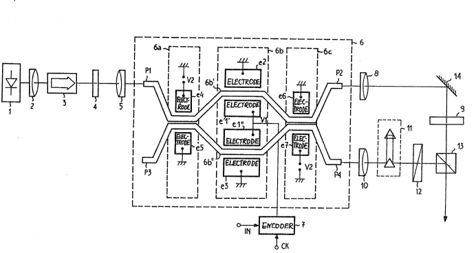
In Fig. 1, the li~ht emitled by a source 1, e.g. a semiconductor laser operating at
15 1550 nm, is collimated by an op~ical system 2 and passes through an isolator 3
preventing radiations reflected by the various modulator elements from returning into
the cavity of laser 1. The radiation outgoing from the isolator, linearly polarized in a
plan~ which can be rotated by a quarter-wave plate 4, is focused by another optical
system 5 at an input of a two-by-two optical switch 6, of any commercially available
20 type. More particularly, owing to the characteristics of the commercially available
optical switches, the input radiation should have horizontal polarization.
In examplary applications of the present invention, the electrical signal
controlling switohing in switch 6 may ba a binary signal, of which the two logic values
corr0spond respeotively to a null voltage and to switching voltage V1 of switch 6. That
25 signal is obtained by coding in an on-off encocier 7 the information to be transmitted.
Arrows IN, CK schematize the inputs for the information signals and for synchronism
signals timing the operations of ~ncoder 7.
A collimating optical system 8 and a half-wave plate 9 for rotating by 90 the
polarlzation plane of the light em2rging from switch ~ ara placed on the path of the light
30 outgoing from P2. On the path of the light out~oing from P4 there are provided, besides
collimating optical system 10, an optical delay line 11 to k~ep the optical lengths of
both paths equal ancl hence to main~ain the coherence among the radia~ions sent along
sald paths, and a polarizer 12 for compensa~ing variations of the stats of polarization
introduc~d by delay line 11.
35 The two palhs end at the two inputs of a polarizing b0am splitter 13, i.e a device
transmitting light polarized in a plane and reflecting orthogonally polarized light. More
particularly, beam splitter 1~ is orien~ed so as to transmit the vertical polarization
anci to reflect the horizontal one. The radiation outgoing from splitter 13 is then sent
7t7~
1 towards the receiver. A mirror 14 makes the radialion outgoing from port P2 of. element 6 arrive onto splitter 13.
~. For a better understanding of ~he operation of the modulator according to the
invention it is convenient to briefly summarisa the structure and ~he operational
5 principle of switch 6. As known, the switch is an integrated-optics waveguide structure
3 comprising an input coupler 6a, a Mach-Zender interferometer and an output coupler
6c. Input coupler 6a divides the power associated with an input signal between the
waveguide portions forming interferometer branches 6b', 6b", which act as phase
shifters. The output coupler recombines on either output the signals coming from the
10 two branches of interferometer 6b. Waveguide portions 6b', 6b" are placed between
`, respective pairs of electrodes e1', e2 and e1", e3, respectively. Electrodes e1', e1" are
connected to the source of switching voltage V1 li.e. to encoder 7, in the described
application), while electrodes e2, e3 are grounded. Also the waveguide portions forming
:. couplers 6a, 6c are placed between respective pairs of electrodes e4, e5 and e6, e7,
15 respectively: an electrode of each pair is grounded and the other is connected to a source
of a voltage V2 (identical for the two couplers), allowing the couplers to be tuned to the
wavelength of the light source used. The connection of the electrodes to voltage V2 is
opposite in the two couplers. Light entering the switch through one of the inputs, e.g.
;~ P1, is equally divided between the interferometer branches. In the absence of voltage
20 V1 ~bit 0 of data signal) and assuming that both branches have the same length, at the
output coupler ihere is phase match between the signals coming from the ~wo branches.
Voltage V2 causes constructive i~terference in interfarometer branch 6b" connected to
P4 and destructiv~ interference in branch 6b' connected to P3, so that a signal is
present only at output P4 (cross state). In the presence of voitage V1 (bit 1), and
25 always assuming equal lengths for both branches. Iight passing in upper branch 6b'
undergoes a + 7~/2 phase shift and light passing in lower branch 6b" a -~/2 phase shift:
the total phas~ shift is 7~, hence the situation in the output coupler is opposite to the
preceding case and light outgoes frorn P2 (straight through state).
That stat0d, ~ha operation of the device according to tha invention is as follows. At
30 a given instant, the light polarized in a horizontal plane en~ering switch 6 through
input P1 outgoes from P2 or P4 according to whether ~he bit of the sequence generated
by encoder 7 has logic value 0 or 1. Whatever thc act3ve oulput, the polarization state
is always the same as that of the input signal of switch 6. If output P2 is active, the
radiation ernitted therefrom is converted into a radiation with vertical polarization by
35 half-wave plate 9 and is transmitted through splitter 13. If output P4 is active. the
radiation arriving at the splitter has maintained its horizontal polarization and hence is
o reflected. Thus, ~he radiation outgoing from splltter 13 has vertical or hori~ontal
O polarization according to whether 1he bit of ~he information sequence is 1 or 0. The
~,
O
7~
1 polarization-modulated signal thus obtained is then demodulated in Ihe receiver of the
communications system, e.g. with the modalities described by R. Calvani, R. Caponi et F.
Cisternino in the paper ~Polarization phase-shift keying: a coherent transmission
technique with differen~ial heterodyne detection~, Electronics Letters, 12 May 1988,
5 Vol. 24, No. 10.
It is clear that the device described satisfies the above-cited requireme~nts.
Optical switches are3 commercially availabla and, since3 they are made3 wilh integrated-
~- optics techniques, they satisfy simplicity and compactness requireme3nts. Besides, as
'' known, they present very short switching times, permi~ting transmission rates of the
10 order of the Gbi~s/s.
In the case of propagation guided in an optical fibre, the modulator has the
structure shown in Fig. 2. Input P1 and outputs P2, P4 ot switch 6 ar~ associated with
corresponding trunks 15, 16, 17 of polarization-maintaining (or highly birefringent)
optical fibre, directly connected to the output of isola~or 3 and repectively to the inputs
~3 15 of a polarization maintaining coupl~r 113, havin~ the sama tasks as splitter 13. It is to
,~ be appreciated that switches like that described can b0 equipped during fabrioation with
fibre portions, to which trunks 15, 16, 17 can be connected. Msreover, modules
comprising the source and the isolator and equipped with a fibre portion for connection
to an optical fibre are also commercially available. Fibre trunks 16, 17 connected to
~ 20 the switch outputs must have the same length to ensure equal optical paths for the
;;~ output signals from the switch to coupler 113. Trunk 15 is mounted on a support
3 allowing its end portion to be rotat~d, as sche3matized by arrow F1, to ensure that the
mode propaga~ing according to the horizontal polarization axis is excited. One at leas~ of
the two output fibre trunks, e.g. trunk 16, is also associate3d with a support of that kind
3' 25 (as schematized by arrow F2), to arrangfl its end portion so that the polarization plana
of the outgoing radiation is the vertical one. If desired, a similar support can be
provided for fibra 17 to ensure that the polarization pianz of the outgoing radiation is
horizontal.
In that embodiment the half-wave p~ates are no longer necessary, and are replaced
~, 30 by a suitable fibre end orientation. Also delay line 11 can be dispensed with, since the
~wo fibre trunks 16, 17 have the same length. The operation is e3qual to that of the
preceding embodiment.
In the variant shown in Fig. 3, rel~vant to the case of fres-space propagation,
switch 6 has been replaced by an integrated optics device comprising only coupler 6a
35 and phase shifters 6b', 6b''. The latter are directly connected with outputs P2, P4. The
paths of the radiations outgoing from P2, P4 end at splitter 13, as in Fig. 1. Splitter 13
8is followed by a quarter-wavs plate 18, which is to compensate phase differences among
iithe output fields of the input coupler and to make the phase of the moduiator oulput
o
~O .
; :n~7~73
- 1 signals depend solely on the eleclro-optic action of voltage V1. The other modulator
components remain unchanged, and are denoted by the same references as in Fig. 1. Of
course, the modification shown in Fig. 3 can be made also for the embodiment of Fig. 2.
-. The operation of this variant is as follows: the light entering through P1 is divided
5 in equal parts betwe~n the two guides 6b~, 6bn, as in the previous case. Output coupler
6c (Figs. 1 and 2) i5 lacking, thus there is no recombination of the signals present in
the two guides, so that both outputs P2, P4 are active at the same time. The signals
'f`J outgoing from P2 and P4 arrive with orthogonal polarizations at split~er 13, whose
output signal will present two orthogonally-polarized cumponents. The relative phase of
10 such components depends on the input signal phase and on the possible phase shift
introduced by guide portions 6b~, 6b~. More particularly, in case of bit 0, the two
components do not undergo phase shifts in guide portions 6b', 6b" and will be in phase
at the output of quarter-wave plate 18 whicil, as mentioned, compensates possible
, phase shifts introduced by the input coupler; in case of bit 1, the two components are
15 phase shifted by +~/2, respectively, by guides 6b~, 6bn, and plate 18 will cause said
,,.~ components to be actually out of phase by +,~/2 and -7~/2, respectively, with respect to
the case of bit 0.
Fialds with symmetrically phase-shifted components can be of advantage in case of
~, polarization phase-shift keying transmissions, since the signal-to-noise ratio can be
1 20 improved by sui~able filters, as described by R. Calvani, R. Caponi, F. Cisternino, G.
`j3 Marone and P. Poggiolini in the paper "Polarization phase shift keying for coherent
optical transmissions with diffsrential heterodyne detection", presented at the
~ International Workshop OCTIMA, Roma, 24-26 January 1989.
- The charac~eristics of simplicity and compactness of the embodiment of Figs. 1 and
25 2 are clearly present also in the embodiment of Fig. 3. A device like that formed by
coupler 6a and phase shifters 6b~, 6b~ can be made by 1he same process leading to the
manufacture of an optical switch, simply by interru;3ting the cioping in correspondence
with the ends of guides 6b', 6b".
It is clear that what described has been given only by way of non limi~ing example
30 and that variations and rnodifications are possibl~ without going out of the scope of the
~ inv0ntion.
`1~ i-.g., phasc-shiftars 6b', 6b" can have different lengths and introduce phase shifts
wi~h different absolute values which need not to be 0 or 7~/2; however, simply by acting
on the voltage supplied to electrodes e1', e1", the phase shif~s introduced by a bit 0 and
35 by a bit 1 can b0 actually 0 and ~/2, or more generally, for the case of Fi~s. 1 and 2,
the signals at the output coupler can be out-of-phase by ~.
Moreover, even if in the preceding description reference has been made to a
binary modulating signal, the invention can also be used in connection with rnul~ilevei
: m
:i
:
' signals. In that case, the optical paths in ~uide portions 6b, 6b will have lengths
depending on the voltage values associated with the different leveis of the information
signal. Consequently, also the phase shifts caused by such guide portions will depend on
the levels of the information signal. For instanca, considering again a symmetrical
` 5 structure and assuming that the information signal has n equally spaced levels and that
vol~ages 0 and V1 are associated with the lowest and the highest level, respec~ively,
such lowest and highest levels will causa phase shi~s 0 and ~/2, respectively, in the
signals travelling along guides 6b, 6bn, whereas the intermediate levels will cause
;, phase shifls differing each by ~=~n, in absoluta value, from the phase shift caused by
10 an adjacent level.
In the embodiments of Figs. 1 and 2, taking into account that the electric fields at
the switch outputs are proportional to sin~ and cos~, respectively (as it can bedemonstrated by simple theoretical considerations), constructive or destruc~ive
interference will occur at Ihe output coupler in correspondence with the lowest ot the
~, 15 highest signal level (as in the case of a binary information signal), and hence only one
switch output will be activa; at the intermediate levels, the output coupler will share
the optical power present at the end of guide portions 6b, 6b among the two ou~puts
and a signal will be present on both paths leading to splitter 13 or coupler 113: the
output signals of such splitter or coupler will exhibit states of polarization regularly
- 20 distributed between the horizontal and vertical linear polarizations. In the embodiment
of Fig. 3, the output signals of the splitter or coupler wiil compri~e two or~hogonal
components with di~ferent relative phase shifts, varying in steps of 21~1n when passing
from one level ~o the adjacant one of the modulating signal. In other words, states of
polarization are obtained which are represen~ed by regularly spaced points on a
25 maximum circlc in the so called Poincar~ sphsre.
The amplitude modulation performed by the switch shown in Figs. 1 and 2 could
,also be obtained by input coupler 6a alone, provided it receivas as control signal a
signal representativa of the modulatin~ signal (more particularly, a voltage having two
different values, e. 9. 0 and V, in correspondence with the two logic values of a binary
30 in~ormation signal, or a voltage varying in steps from a minlmum to a maximum valua,
in case of a multilevel information signal). Thus, in the case of multilevel signals, if
both Input coupl~r 6a and phase shifter 6b ara controlled by respective si~nals obtained
from the information signal through a suitabi~ sncoder, both the relative phasa of the
signals arriving at the two output ports and the amplitude ratio of same can be made
35 dependent on the modulating signal level. That further degrse of freedom allows any
statfl of polarization to be obtained at the modulator outpu~, i. e. polarization signals are
oobtained which ar~ reprssanted by point arrangad in any manner on the Poincare
Osphera. The two control signals can bs obtained from respec~iva ~roups of the bits of a
n
5o
~6~ t~,3
1 binary representa~ion of the different levels of the modulating signal: for instance, in
case of a 4-level signal (whose levels can be represented by 2 bits), the less
significant bit can be used to control the ampli~ude and the more significant bit the
phase; for a signal with more than 4 levels, the least significant bit of the level
5 representation can be still used to control the amplitude and the other bits to control the
phase, and so on.
', .
~ .