Note: Descriptions are shown in the official language in which they were submitted.
38~
- 1 - 45MR00592
E~ECTRICALLY-TUNABLE BANDPASS FILTER
FIELD OF THE INVENTION
This invention relates genarally to bandpass
filters. More particularly, the invention relates to an
electrically-tunable bandpass filter that may be
advantageously utilized as a narrow RF bandpass filter
in a radio receiver which may be tuned automatically by
~arying a single control voltage.
BACRGRO~ND AND SUMMARY OF THE INVENTION
A radio receiver is designed to be extremely
sensitive to responding to the desired signals to which
it is tuned and to rejecting signals to which it is not
tuned. Superheterodyne radio receivers typically
achieve the bulk of their selectivity using narrow
fixed-tuned intermediate frequency (If) filters. These
filters reject undesired signals which may be present at
RF frequencies which are close to the desired or "tuned"
frequency. Such narrow if filters do not prevent the
reception of undesired signals which are converted in a
mixer directly into the If passband. Such undesired
signals which are not rejected by the radio receiver
filters create spurious responses such as image, half If
and intermodulation (intermod) distortion.
These spurious responses may be generated in
.
.
- ~ ~ ' ' ' ' ,
'' ,
- 2 - ~5~R00592
part due to the operation of the mixer in which various
mixing products are genera~ed, one of which is at the
desired If frequency. One approach to eliminating such
spurious responses is to use bandpass filters to prevent
unAesired signals from reaching the mixer in the super~
heterodyne radio receiver.
In the past, it was common practice to use a
very narrow RF bandpass filter to prevent such undesired
signals from reaching the mixer. Such "front end
selectively" was effective at eliminating most spurious
responses, but the resulting receiver could only be
operated over a very narrow band of desired receive
frequencies without retuning the narrow RF filter.
Thus, although narrow RF bandpass filters are effective
in eliminating, for example, image and half If spurious
responses, such prior art filters are limited to
receiving a narrow band of frequencies and cannot be
reconfigured automatically to receive signals over a
wide frequency band.
Many modern day receivers utilize a much wider
~ront end filtering system designed to pass the entire
band of frequencies to which the receiver may be tuned
(e.g., 150-17~ MHz for a particular band used in the
land mobile radio service). By careful design and
pxoper selection of the If fre~uency, such a wideband
filter can be designed to provide adequate protection
from image and half If spurious responses. However, a
wideband front end filtering system greatly increases
the incidence of intermod distortion in the receiver by
allowing a much larger number of in-band signals to
reach the mixer.
Such an intermod spurious response is created
when two or more undesired signals reach a non-linear
element in the receiver such as the first mixer and
combine to create a product that is directly on channel.
. . .. .
- ~
.
- 3 - 45MR00592
Accordin~ly, such an on-channel signal cannot be readily
distinguished as an undesired si~nal. Such undesired
si~nals, which are mixed to produce an on-channel
signal, may be so close to being on-channel themselves
r~ that they are difficul~ ko reject with a wideband
filter.
Various ~ilter desi~ns have been used
heletofore to provide an automatically tuned front-end
filter. Each such design, howaver, has significant
la disadvantages, particularly, for example, in regard to
satis~ying the needs of a mobile or portable radio
communications system.
In broadcast receivers, a mechanically
variable capacitor havin~ two or more sections which are
~'qanqed to~ether" is used to tune the local oscillator
and front end filter simultaneously~ While such an
appxoach may be acceptabla in an AM broadcast radio
receiver, where the bandwidths are very wide, this
approach is not suitable for mobile radio receivers
which have extremely narrow channel spacing and which
cannot tolerate the poor frequency stability of such a
mechanically tuned local oscillator. Thus, in a mobile
radio receiver, if the filter detunes or the local
oscillato~ drifts by any small amount due to such poor
~a ~requency stability, desired signals may not be
received.
Another approach which heretofore has been
utilized to provide an automatically tunable front end
filter, uses multiple front end filters, each of which
~5 is tuned to a different frequency within the overall
passband. Such a system includes control circuitry in
the receiver ~hich selects the appropriate filter based
on the radio channel selected and switches it to the
front end via, for example, a relay or a PIN diode
switch. Each of the multiple front end filters is
.
3'7~
- ~ - 45MR00592
typically a narrow fixed tuned filter. In order to
effectively cover a wide band of frequencies using such
narrow filters, a large number of filters is required.
Accordingly, such a design from a practical point of
view is prohibitively costly, complex and bulky.
A further approach to providing an
automatically tuned front end filter incorporates
voltage variable capacitors (i.e., varactor diodes) as
reactive elements in a single filter. A control voltage
1~ is applied to the varactor diodas to tune the filter to
the desired receive frequency. This approach has
heretofore typically utilized a reactively coupled
resonator filter which generally has multiple sections
that are tuned separately but which must "track" as the
1~ tuning voltage varies. Such a multiple section filter
must have sections which have the same tuning response
so t~lat each section tunes in ~xactly the same way when
t~e tuning voltage varies. To ensure that such
"tracking" takes place in the proper fashion adds to the
~0 complexity of the filter. Additionally, although such a
filter may be effective to reduce image and half If
spurious responses, in such prior art tunable filters
which incorporate varactor diodes, the diodes tend to be
subjected to high RF levels at all frequencies and have
~5 the potential to generate intermod products themselves.
The present invention overcome many of the
above-mentioned problems associated with conventional
radio receiver filters in superheterodyne radio receiver
applications. The present invention provides a narrow
front end filter which can be tuned automatically as the
local oscillator frequency is changed. In this fashion,
the present invention reduces the number of spurious
responses in the radio receiver while still allowing it
to tune automatically over the full range of the desired
fre~uency band.
.
,,
.. . :
.
' - ' ' : ~ :
.
2~ '7~
- 5 45M~00592
In this regard, it is noted that the tuning
~oltage is used to control a single point in the circuit
of the exemplary embodiment of the present invention.
The tuning voltage is input at the junction between two
varactor diodes which are placed back to back to thereby
provide more linear tuning of center frequency versus
voltage while providing higher intermod immunity than
would be available using a single varactor diode.
~dditionallyr the need for "tracking" between multiple
1~ diode sections is avoided. In the present invention,
the varactor diodes are significantly decoupled from
high RF levels. This results in less voltage being
coupled across the varactors, reducing the possibility
of generatin~ unwanted intermod products.
1~ The electrically tuned bandpass filter of the
present invention uses the signal isolating properties
of a balance resistive brid~e to transform a series
tuned reflective notch filter into a selective bandpass
filter. While any directive device such as a
~0 directional coupler, ferrite circulator, Wilkinson
splitter, etc., could be used to provide this
transformation, the resistive bridge of the exemplary
embodiment additionally operates to provide an apparent
"Q n~ultiplication" in the tuned circuit yielding a
sharper selectively curve.
In the present exemplary embodiment, the
series tuned reflective notch filter is coupled to a
node of the balanced resistive bridge in such a manner
that the tuned circuit presents a short circuit to the
node at the filter's resonant frequency to thereby
assure a maximum transfer of signal from the input to
the output of the circuit at a desired frequency. At
all other frequencies, however, the series tuned
reflective notch filter will present essentially an open
circuit across the node of the resistive bridge so that
: . .
- 6 - 45MRoos9?
the node is balanced and no transmission occurs. The
inclusion of the series re~lective notch filter thereby
produces a bandpass characteristic from the circuit
input to output.
By using varactor diodes in the reflective
notch filter, the center frequency of the passband can
be changed by changing the tuning voltage applied to the
varactors. In the configuration of the present
invention, the varactor diodes are protected from high
signal levels which are not within the narrow passband
o~ the filter. For this reason, the ~ilter is
inherently less susceptible to the generation of
intermod products than filters of a conventional design.
BRIEF DESCRIPq!ION OF THE DRAWIN&S
These as well as other objects and advantages
of this invention will be better appreciated by reading
the following detailed description of the presently
preferred exemplary embodiment taken in conjunction with
the accompanying drawings of which:
~a FIGURE 1 is a block diagram of a portion of a
radio receiver system in which the bandpass filter of
the present invention may be advantageously utilized;
and
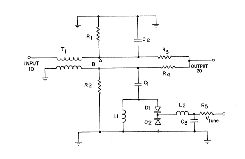
FIGURE 2 is a schematic diagram of an
~5 axemplary embodiment of a bandpass filter in accordance
with the present invention.
DE~AILED DESCRIPTION O~ THE DRAWINGS
The presently preferred application for the
bandpass filter of the present invention is in a
superheterodyne radio rec~iver. In such a radio
receiver system, a portion of which is generally
represented in Figure 1, a radio frequency signal is
received by antenna 1 and is coupled to front-end
,: . ~' . ' ' ;
.
- , ' - ~ " ~ . '
- 7 - 45MR00592
preselector 2.
The bandpass filter of the present invention,
an exemplary embodiment of which is shown in Figure 2,
may be disposed within front-end preselector 2 which
5 comprises filters and other associated circuitry which
set the sensitivity of the receiver. The preselector 2
serves to filter unwanted signals ~o prevent such
signals ~rom being input to the first mixer L~. Within
preselector 2, a conventional wideband filter (not
shown) is coupled to antenna 1. The output of the
wideband filter is coupled to a conventional RF
amplifier (not shown~ whose output is coupled to input
port 10 of the exemplary bandpass filter shown in Figure
2. The output signal from output port 20 of the
bandpass filter of the exemplary embodiment is coupled
to mixer 4 shown in Figure 1.
Mixer 4, as is conventional, heterodynes the
local oscillator signal with the incoming signal to
generate sum and difference signals. The output of the
~0 first mixer includes, for example, a difference output
fre~uency which may be the intermediate frequency
signal.
The output of mixer 4 is amplified by an
intermediate frequency amplifier 6 which is tuned to
~5 ampli~y signals in the desired intermediate frequency
range. The amplified intermediate frequency signal may,
for example, then be coupled to the If processing
subsystem 8 of the radio, where the signal is further
filtered and amplified. The filtered and amplified
signal may then be applied to a second mixer, where it
is further down converted to form a second If-frequency
signal. Thereafter, the signal of interest is detected
via a conventional FM (or AM) detector. Such an If
processing subsystem is conventional and forms no part
of the present invention.
.
.
'
8~'7~
- 8 - 45MR00592
The bandpass filter of the exemplary
embodiment of the present invention is shown in ~igure 2
and includes an input port 10 and an output port 20.
Coupled to the input port is a transformer Tl.
Transformer Tl may, for example, be a wideband
transmission line transformer which ac~s as a one-to-one
transformer in order to isolate the ground to thereby
create a floating ground. Thus, if a signal Vl is input
at port 10, instead of varying, for example, from 0 to
Vl ~olts at node A, the output signal from transformer
T1 swings from -V1/2 to +V1/2 at node A and from +V1/2
to -Vl/2 at node B.
The amplitude of the voltage variations with
respect to ground are the same at nodes A and B but are
180 degrees out of phase. This amplitude being one hal~
o~ the amplitude which would be present at A if B were
grounded. The transformer T1 primary is coupled to node
A, which is coupled to resistor R1, which in turn is
coupled to ground. The primary of transformer T1 is
also coupled to output 20 via resistor R3.
Node A and resistor R3 are also coupled to
capacitor C2 (which compensates for stray capacitance as
will be explained further below), which in turn is
coupled to ground in parallel with resistor Rl.
Resistor R3 is also coupled to resistor R4 which is
coupled to node B, which in turn is coupled to the
grounded secondary coil of transformer T1. Node B is
additionally coupled to resistor R2 which is also
coupled to ground.
As will be explained in detail below,
resistors Rl, R2, R3 and R4 form a balanced resistive
bridge. Coupled to node B of the balanced resistive
bridge is a series tuned re~lective notch filter.
In the exemplary embodiment shown in Figure 2,
the notch filter includes a capacitor C1 which is a
- ~ . ,
- 9 - ~5~R005~2
small ~ixed capacitor which may, for example, be 1.5
picofarads. capacitor C1 is coupled to inductor L1
(which may, for example, be an RF coil of 181 nH), which
is also coupled to ground. Capacitor C1 is ad~itionally
5 coupled to the anode of varactor diode D1, whose cathode
is coupled to the catllode of varactor diode D2, whose
anoda is coupled to ground. Diodes D1 and D2 may, for
exalllple be ~otorola Model No. MMBV105G varactor diodes.
Varactor diodes Dl and D2 form a voltage
l~ variable capacitor which is parallel resonant with L1,
at a frequency above the desired tuning frequency of the
~iltex. Thus, at the desired frequency, the parallel
combination of Ll and Dl and D2 appears to be a high
value of inductance which can be varied by varying
1~ VtUne~ This inductance in turn resonates with capacitor
Cl to yield a low series impedance at the desired center
~re~uency~ VtUne is coupled to the cathodes of varactor
diodes Dl and D2 via resistor R5 and inductor L2 which
are coupled to ground through capacitor C3.
2 a Focussing on resistive bridge Rl, R2, R3 and
R4, as noted above, the signal at nodes A and B swings
between ~Vl/2 and -V2/2. If the ratio of resistances Rl
to R2 is chosen to be equal to the ratio of resistances
~3 to R4, then the voltage developed from node A to
2~ ground across Rl will be the same as the voltage
developed from node A to output 20 across R3.
Similarly, the voltage from node B to ground across R2
will be the same as the voltage developed from node B to
the output 20 across R4. In both cases the resulting
voltage at output 20 is at ground potential. Under such
conditions (ignoring for the moment the notch filter),
there will be no output voltage at output port 20.
Thus, by proper selection of resistors R1, R2, ~3 and
~4, to achieve a balanced resistive bridge, it is
possible to prevent any output voltage from being
,
- 10 - 45~R00592
developed at node 20, irrespective of the applied input
voltage.
In the present exemplary embodiment, notch
filter (~1, Ll, Dl and D2) operates to disturb the
balance effect of the resistive bridge, such that at a
predetermined desired frequency an output signal begins
to develop at output port 2 0 . In this regard, the notch
filter Cl, Ll, Dl and D2 operates as a reactive element
which is placed across resistor R2 and serves to short
out xesistor R2 at a predetermined desired frequency.
The notch filter Cl, Ll, Dl and D2 operates
substantially as a short circuit for a narrow band of
input frequancies and as an open circuit at all other
fre~uencies.
1~ With the resistor R2 shorted out at the
particular frequency, the resistive bridge Rl, R2, R3,
and R4 is then out of balance and a signal appears at
the output port 20. Thus, when ~he notch or band
elimination filter Cl, Ll, D1 and D2 i5 utilized in
~0 conjunction with the resistive bridge network as shown
in Figure 2~ a bandpass filter is created.
By coupling VtUne to the notch filter at the
cathodes of varactor diodes Dl and D2, the bandpass
~ilter may be readily tuned. In this regard, the
~5 fre~uency at which an output signal is generated at
output port 20 is determined by the series resonance of
capacitor Cl with the equivalent inductance of L1 in
parallel with varactor diodes D1 and D2. The resonant
~requency may be changed by changing the tuning voltage
VtUne which operates to vary the capacitance of varactor
diodes Dl and D2 to thereby change the series resonance
frequency of the notch filter network.
Focussing back on the resistive bridge network
Rl, R2, R3 and R4, this network is comprised o~
resistors whose values have been chosen to minimize the
.
' . '
- '
.
.
3>~
~ 45MR00592
insertion loss in the passband of the signal being
transmitted from the input port 10 to output port 20.
In this regard, resistor Rl may, for example, be 220
ohms, resistor R2 may, for example, ba 1800 ohms,
5 resistor R3 may, ~or example, be 27 ohms, and resistor
R4 may, for example, be 220 ohms. R2 has been chosen to
be a relatively large resistance value so that at
resonance when ~he balance of the bridge is disrupted by
notch filter C1, Ll, ~1 and D2, which presents a short
circuit in parallel with R2, the residual resistance of
the short circuit will be negligible in comparison with
the resistance R2. In view of this particular choice of
resistor valuesS capacitors C2 (which may, for example,
be 15 picofarads) is necessary to compensate for stray
capacitance which otherwise would impact one side of the
resistive bridge more than the other side.
The resistor values identified above serve to
maintain a 50 ohm input and output impedance in the
passband of the filter. In this regard, when the series
~0 tuned notch filter presents a short circuit to node B,
resistors Rl, R3 and R4 are further chosen to simulate a
m~tched 50 ohm Pi attenuator. Since nominal passband
insertion loss is equal to the value of attenuation
chosen, it is desirable to design for the lowest
25 attenuation possible. The exemplary values for R1, R3
and R4 referred to above correspond to a matched 4.4 dB
attenuator. Thus, the nominal insertion loss of the
filter is 4.4 dB (the actual attenuation may exceed this
due to additional stray losses in the circuit). The
3~ resulting impedance to ground from node B is 86 ohms
compared to 25 ohms for a conventional 50 ohm bridge.
This results in a potential 3.4 fold increase in loaded
Q. It should be recognized that the exemplary 4.4. dB
attenuator was chosen in the exemplary embodiment so the
resistors could be implemented using standard chip
,
.
,
: . -
~ .
, ' ' , ' ~
- 12 - 45MR00592
resistors. By using non-standard resistors and
accurately trimming their values, even lower loss and
higher apparent Q can be achieved.
Focussing now in more detail on the operation
of Figure 2, if an input signal Vl is applied to input
por~ 10, a differential signal is developed by trans-
former Tl, such that +Vl/2 is applied to node A (and Rl
and R3) and -Vl/2 is applied to node B (and R2 and R4).
The signal input at port 10 is split into two paths. On
one path the signal goes through resistor Rl to ground,
through ground to resistor R2 to the bottom coil of
transformer Tl. On a second path the signal at node A
goes through resistor R3 into resistor R4 and back
through the bottom coil of transformer Tl.
1~ ~f the ratio of the resistances Rl to R2 is
e~lal to the ratio of the resistances of R3 to R4, then
the resistive bridge is balanced and no voltage is
developed from output port 20 to ground.
The balance of the resistive bridge is
2-) disrupted by the notch filter formed by Cl, Ll, Dl and
D2 at the resonant frequency of this notch filter
circuit. The series resonance frequency for the notch
filter is chosen to be the center frequency of the
desired passband for the passband filter shown in Figure
2~ 2. By appropriately choosing the values for C1, Ll, Dl
and D2, the notch filter can be designed to be very
selective in disrupting the isolation from input port 10
to output port 20 to (i.e., cause this disruption take
place only ~or a selected narrow band of frequencies).
By only permitting a very narrow band of frequencies to
be transmitted from input port 20 to output port 20, the
notch filter can thereby discriminate against undesired
signals being passèd from input port 10 to output port
20. Thus, signals which would tend to cause intermod
problems or other spurious responses can be precluded
.: - , . . . . .
:'. , ' ,, : :
': . '
- 13 ~ 45MR00592
from passing from input port 10 to output port 20.
The notch filter Cl, L1, Dl and D2 is tuned by
applying a DC voltage to the junction of varactor diodes
Dl and D2. The applied DC voltage changes the reactance
of varactor.1 and D2 to thereby tune the notch filter.
Inductor L2, resistor Rs and capacitor C3 serve to
couple the DC voltage Vtune into the junction o~
varactor diodes Dl and D2. Capacitor ~3 serves to
couple RF frequencies to ground to decouple the junction
1~ of Dl and D2 fxom the tuning voltage input port 30 for
AC fre~uencies. As will be appreciated by those skilled
in the art, other component configurations could be
utilized to couple the ~C voltage VtUne to the junction
of varactor diodes D1 and D2 as shown in Figure 2. In
this regard, L2, Rs, C3 serves as a noise filter to keep
noise signals away from the junction of D1 and D2.
~ther more elaborate noise filters could be utilized in
place of L2, C3 and R5.
It is noted that although the balanced
resistive bridge shown in Figure 2 is the presently
preferred device for isolating input port 10 from output
port 20, the bridge may, if desired, be replaced with
any directive device which has similar signal isolation
properties. Thus, the present invention may be modified
~5 to incorporate any directive device such as a
directional coupler, a ferrite circulator or Wilkinson
splitter which have such signal isolating properties
which may be used to transform a series tuned notch
filter into a selective bandpass filter.
While the present exemplary embodiment has
been described in conjunction with a heterodyne radio
receiver, it should be recognized that the circuit shown
in Figure 2 may be advantageously utilized in
conjunction with any application where there is a need
for a bandpass filter. While the invention has been
2~
- 14 - 45MR00592
described in connection with what is presently
considered to be the most practical and preferred
embodiment, it is to be understood that the invention is
not to be limited to the disclosed embodiment, but on
the contrary, is intended to cover various modifications
and equivalent arrangements included within the sp.irit
and scope o~ the appended claims.
' ~ , '; ' . ,
' ' '
.