Note: Descriptions are shown in the official language in which they were submitted.
2~8~
~HIE~DED cApAcIrA~c~ 8T~DA~D
Fi~ld of the Invention
The invention relates to a device for
standardizing and calibrating capacitance moisture
probes.
Backqround of_~h9 1__entlon
one well known method for measuring
moisture content of materials such as grain, soil~
and the like is by measuring the electrical
capacitance of the material. The electrical
capacitance of the material is directly related to
the dielectric constant of the material. The
dielectric constant of most soil materials and of
dry grain is relatively low. The dielectric
constant of water is significantly hiyher which
substantially affects the overall dielectric
constant of the materials depending on the
concentration of the water in the materials.
Therefore, a measurement of the dielectric constant
or capacitance of a material can serve as an
accurate measurement of the moisture content.
Capacitance sensitive probes are disclosed
in U.S. Patents 4,044,607 to Deal and 4,399,404 to
Resh and in articles by A.M. Thomas, "In situ
Measurement of Moisture in Soil and Similar
Substances by Fringe Capacitance," J. Sci. Instrum.,
Vol. 43, 1966, Pages 21-27 and D. Wobschall, "A
Frequency Shift Dielectric Soil Moisture Sensor,"
20~7~
--2--
IEEE Transactions on Geoscience Electronics, Vol.
~E-16, No. 2, April 197~, Pages 11~ . These
probes generally comprise a pair of electrodes which
are so arranged that the tes~ material functions as
a dielectric between the electrodes. The electrodes
are in an electrical circuit which measures the
capacitance by suitable means such as an oscillating
LC network. Changes in capacitance cause a
measurable frequency shift in the oscillating
circuit and thus can provide an indication of the
moisture content of the soil.
Capacitance moisture sensing probes
however, are by necessity precision instruments. A
slight change in the capacitance of soil may
represent a substantial difference in moisture
content. Therefore, capacitance moisture sensing
probas must be highly sensitive to the capacitance
and must be carefully calibrated to assure that the
measured capacitance is accurately coordinated with
the moisture content.
Because of variations in manufacturing
tolerances, moisture sensing probes of the same
design will not necessarily sense the same
capacitance. Consequently, each capacitance sensing
probe must be individually calibrated and as a
practical matter the probe should be periodically
checked to assure that the calibration has been
maintained.
The most common method to calihrate a
capacitance moisture probe, particularly a probe
used to measure the moisture content of soil, is to
prepare calibration standards with carefully
measured portions of dry sand and water. The probe
is inserted into each of the calibration standards
and the frequency of the oscillating circuit is
recorded. The frequencies then may be calibrated to
correspond to the known moisture contents of each of
20~g-1 ~9
the soil samples. The preparation of the samples
is, however, a tedious and painstaking process which
is prone to errors. Therefore, the probes tend to
be recalibrated infrequently~ if at all.
At least one device has been developed to
provide a suitable substitute to simulate a
particular moisture content. U.S. Patent No.
4,147,976 to Wang discloses a calibrating device
which is compatible with a grain moisture sensor.
The grain moisture sensor has the appearance of a
cup with an upright electrode centered therein. A
second electrode is positioned in the wall of the
cup and the capacitance is measured through the
grain between the electrodes. The calibrating
device comprises a pair of concentric dielectric
tubes which form an annular space. The annular
~pace is sealed at both ends and filled with metal,
liquid or other materials which provide the device
with a predetermined capacitance simulating grain
having a particular moisture content. The
calibrating device is then inserted into the cup and
the capacitance is measured through the annular
space. This type of device is, however, unsuitable
for calibrating moisture probes of the type which
are inserted into the soil because of the geometry
of such probes. The electrodes of soil moisture
probes are typically mounted on the periphery of a
cylinder and are not suitably disposed to measure
capacitance through an annular space. Also, outside
electrical fields have a tendency to affect the
measurement of capacitance by the moisture probe.
This problem is not seriously encountered while down
in the soil, but out in the open it becomas a
greater concern. The Wang device provides no
measure of protection against outside electrical
fields.
2 ~ 7 ~
--4~
~ccordingly, it is an object of the
present invention to provide a capacitance standard
for use to calibrate capacitance moisture probes
which avoids the disadvantages of ths prior art as
notqd above.
It is a more particular object of the
present invention to provide a capacitance standard
for use to calibrate capacitance moisture probes
which provides an inPxpensive reliable capacitance
measurement and which is no~ affected by outside
electrical fields.
SummarY of the Invention
The abova and other objects o~ the
invention have been achieved in the pres~nt
invention by the provision of a shielded capacitance
standard comprising a capacitor having respective
plates and a dielectric cooperating to define a
capacitance of fixed value. The capacitance
standard is provided with means for connecting
electrodes of a capacitance sensitive probe to the
respective plates of the capacitor so that the probe
will measure the fixed value capacitance. The
shielded capacitance standard further has a shield
which cooperates with the capacitor to shield the
capacitor and the probe from external fields so that
the measured capacitance is accurate and
reproducible, facilitating the calibration of
capacitance sensitive probes.
Brief DescriPtion of the Drawinq~
Some of the features and advantages have
been stated and others will become apparent as the
description proceeds when taken in conjunction with
the accompanying drawings, in which:
Figure 1 is a perspective view of the
shielded capacitance standard which embodies the
features of the present invention; and
2~0~:L71'`
--5--
Figure 2 is an enlarged cross-sactional
view of the shielded capacitance standard taken
substantially along the line 2-2 in Figure 1.
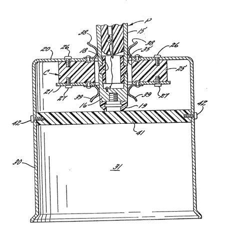
Detailed DescriPtio~ the Preferrecl Embodiment
~eferring now more particularly to the
drawings, Figures 1 and 2 illustrate the preferred
embodiment of a shielded capacitance standard,
generally indicated by the numeral 10. The shielded
capacitance standard 10 is used in conjunction with
capacitive sensitive probes for facilitating
calibration thereof. In the illustrated embodiment
(Figure 2), the capacitance sensitive probe P is
generally aylindrical in shape with electrodes
spaced apart by a dielectric. Briefly, probe P
comprises first and second electrodes 15 and 16
spaced apart by a dialectric spacer 18. A
dielectric tip 19 is attached to the electrode 16 so
as to space the electrode from the end of the probe
P. The electrodes are electrically connected to an
electronic circuit (not shown) for measuring the
frequency shift in an LC circuit. The probe P is
primarily intended for measuring the ground moisture
content of soil and to obtain optimum contact with
the soil the probe has a slight taper which will be
accommodated by the capacitance standard as
explained below.
The preferred embodiment of the
capacitance standard includes a capacitor C
comprising a metallic first plate 20 and a generally
parallel metallic second inner plate 21 spaced apart
by a dielectric 25. The dielectric 25 is attached
to the first plate 20 in an overlyiny manner by
conventional means such as screws 26. The second
plate 21 is similarly attached to the dielectric 25
in an overlying manner by screws 27. The
capacitance of the capacitor C is a fixed value
which is the result of a combination of the size and
200~
--6--
shape of the plates, the thickness of the
dielectric, the dielectric constant of matarial or
materials used in the dielectric and other factors
known to persons having ordinary skill in the art.
In the preferred embodiment, ~he plates are made of
stainless steel, aluminum or other corrosion
resistent metal~ The dielectric is formed from a
block of a hydrophobic polymer material having a
relatively high dielectric constant. Since the
polymer material is hydrophobic, haviny little or no
a~finity for water, its dielectric properties do not
fluctuate with fluctuations in ambient humidity. A
preferred polymer material having these properties
is polyethylene, or a polyvinylidene fluoride
material. These materials are relatively rigid and
durable so as to maintain a constant spacing between
the plates 20 and 21.
The shialded capacitance standard 10
comprises a metallic enclosure having a top portion
20 and a side wall portion 30 defining an enclosed
shielded space 31. The top portion 20 of the
enclosure also serves as the first plate of the
capacitor. ~he dielec~ric 25 and second plate 21
are disposed within the enclosed shielded space 31
so that the capacitor is shielded from outside
electrical fields which might affect the measurement
of the capacitance value of the capacitor. In the
preferred embodimant the upper portion 20 of the
metallic enclosure and the enclosing wall 30 are
integrally formed and define a generally cylindrical
enclosure.
As illustrated, a hole 35 is located in
the central portion of the first plate 20 and
extends through the dielectric 25 and the inner
plate 21 for receiving the probe P down into the
shielded space 31. Thus, when a probe P is inserted
into the hole as shown in Figure 2, the electrodes
:~ ~ o ~
15, 16 of the probe are loca~ed interiorly of the
shielded enclosure and are therefore shielded from
outside electrical fields as is the capacitor~
Contacts 38 are mounted on the upper surface of
plate 20 and are disposed around the hole 35 Eor
providing electrical contact between the electrode
15 and the plate 20. Similarly, contacts 39 are
mounted on the exposed under surface of inner plate
21 and are arranged around the hole 35 for
n contacting the electrode 16 of probe P. The
contacts have a shape generally similar to the shape
of a IIC'I and are made of spring steel or other
flexible conductive material to be spring ~iased
toward the hole. The contacts therefore bend and
conform to the dimension of the probe and
accommodate variations in the diameters of the
probes as well as the taper of the probe P. The
contacts are fixed to the plates by conventional
means such as rivets. In this arrangement, as
clearly shown in Figure 2, ~he capacitor C bridges
across the electrodes 15 and 16 so that a
capacitance measurement taken by probe P is that of
the capacitor.
To provide proper alignment of the
electrodes with the contacts, a stop 41 is mounted
within the shielded enclosure extending beneath the
hole at an appropriate distance to limit the depth
the probe may be inserted into the hole 35. The
stop is secured to the wall 30 by suitable fastener
means, such as bolts 42. In the preferred
embodiment, the stop 41 is formed of a nonconductive
dielectric material so as to be electrically
insulated from the probe, even if the probe should
be electrically conductive at the tip. The
dielectric material is preferably a polyethylene or
polyvinylidene fluoride material, although other
suitable materials may be used.
~008~
In use, several capacitance standards are
provlded having a range of capacitance values
covering the range o~ moisture contents which are to
be measured. The probes may be calibrated over the
range of moisture contents by measuring the
capacitance o each standard and e~,tablishing
therefrom appropriate cali~ration curves or
eguations relating the capacitance reading of the
probe to a moisture content reading.
The foregoing description is to be
considered illus~rative ra~her than restrictive of
the invention, and those modificatlons which come
within the meaning and range of equ.ivalence of the
claims are to be included therein.