Note: Descriptions are shown in the official language in which they were submitted.
2oos552
INFORMATION SEPARATION DEVICE
Field of the Invention
The present invention relates to an information
separation device which has a transformer operating as a
separating filter to separate transmitted alternating voltage
information signals from direct current power. The informa-
tion separation device has at :least one winding on the side
blocking direct current with a storage capacitor being
serially coupled to the winding.
Background of the Invention
Bus systems are known having various designs and
implementing various types of transmission (see DE-A-3 631
477). In bus systems digital data can be transmitted for
measuring or controlling or analog signals can be transmitted.
Bus systems are also suitable for voice transmission, as is
discussed in European Patent Application EP 88117678.8.
There are known systems that have stations which can
either process data or operate sensors, wiring accessories or
motor-driven equipment like venetian blinds. These stations
are coupled to a bus via a bus-coupler. The systems are
designed either in a centralized or decentralized manner.
Either digital data or analog signals can be transmitted over
the bus for measuring or controlling the signals. In addition
to the information, i.e., messages, sent to the stations,
power for the electrical apparatus of the system is also
supplied via the bus-coupler. In addition, the power
available to the end user is also to be supplied to energy
_1_
20365-3013
2008552
consumers such as motors, lights or heating devices.
The interplay between the bus and the bus-couplers,
the number of required transmission paths as well as the type
and operation of the devices effect the economic efficiency of
a bus system. There is a need for an information separation
device that operates especially economically.
Summary of the Invention
This and other needs are met by the present
invention which provides an information separation device
having a transformer operating as a separating filter
separating transmitted alternating voltage information from
direct current power. The transformer has a first side and a
second side, the first side having at least one first winding
and a capacitor coupled in series to the first winding, this
capacitor blocking direct current. The second side of the
transformer has a second winding with first and second ends
and processes received separated information. First and
second transistors are arranged parallel to the storage
capacitor in a transmitting branch, with the second winding
being coupled at its first between the first and second
transistors first and second diodes are arranged in a branch
parallel to the storage capacitor, the second winding being
coupled in series between the first and second diodes in phase
opposition to the first and second transistors in the
transmitting branch.
In this manner, power stored in the second winding
can be recovered and brought to the other side of the trans-
former, whereby the transformer is bypassed. With this method
-2-
20365-3013
CA 02008552 1999-09-22
of energy transport, the transformer is relieved so that it
can be more compactly and economically designed and allow the
point of operation to be more favorable.
In prior systems, separate individual winding's would
be necessary for transmission and for power recovery. In the
present invention, one winding is used for both functions.
According to an embodiment of the present invention,
one of the transistors in the transmitting branch is
controlled to be conductive for standby receiving during
breaks in transmission while the other is kept in the blocking
state, and the receiving signal is picked off from the end of
the second winding to which the conductively-controlled trans-
istors valve is not coupled. With this type of information
separation device, the single winding used for transmission
and power recovery is also used for the reception signals.
Usually, an additional individual winding is needed for this
purpose. Instead, the device according to the present inven-
tion for the transmission and reception signals with simultan-
eous power recovery from the winding does this with a single
winding. The information separation device of the present
invention is therefore suited for the transmission of messages
and for the transmission of power on a common line, especially
for a two-conductor bus. However, other transmission paths
and systems are also usable with the present invention.
-3-
20365-3013
CA 02008552 1999-09-22
In accordance with the present invention, there is
provided an information separation device comprising: a
transformer which separates transmitted alternating voltage
information from direct current power, the transformer having a
first side and a second side, said first side having at least
one winding and a capacitor coupled in series to said winding,
said capacitor blocking direct current; said second side of said
transformer having a winding with first and second ends and
processing received separated information; first and second
l0 transistors arranged in a transmitting branch parallel to said
capacitor, said winding of said second side of said transformer
being coupled at its first end at a point between said first and
second transistors; first and second diodes arranged in a branch
parallel to said capacitor, said winding of said second side of
said transformer being coupled in series at its first and second
ends between said first and second diodes in phase opposition to
the first and second transistors.
In accordance with the present invention, there is
further provided an information separation device comprising: a
20 means for separating transmitted alternating voltage from direct
current, said means for separating has a first side and a second
side; at least one winding, located at said first side of said
means for separating; a means for blocking direct current,
connected in series with said winding; a means for storing
power, located at said second side of said means for separating
and having a first and a second terminal; a first means for
switching, having an on state providing a positive voltage at
said first terminal of said means for storing power and a
negative voltage at said second terminal of said means for
30 storing power; a second means for switching, having an on state
providing a positive voltage at said second terminal of said
means for storing power and a negative voltage to said first
3a
20365-3013
CA 02008552 1999-09-22
terminal of said means for storing power; wherein said first
means for switching is on and said second means for switching is
off during a break in a transmission and said first means for
switching is off and said second means for switching is on when
a positive transmission signal is present.
Brief Description of the Drawi
FIG. 1 shows a circuit of an information separation
device constructed in accordance with an embodiment of the
present invention.
3b
20365-3013
2008552
FIG. 2 shows a circuit of an information separation
device constructed in accordance with another embodiment of
the present invention.
Detailed Description
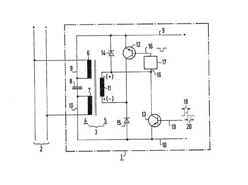
An embodiment of an information separation device 1
is shown coupled to a bus 2 in FIG. 1. This bus 2 also
carries direct current for the supply of the electrical appar-
atus systems of the station 1 and additional information
separation devices that can also be coupled in parallel on the
bus 2. The bus 2 also carries alternating voltage information
signals for the communication traffic. The information
separation device 1 has a transformer 3 operating as a
separating filter to separate transmitted alternating voltage
information from direct current power. On the side 4 of the
transformer 3 which is connected to the direct current power,
there are two windings 6 and 7 for reasons of symmetry. A
capacitor 8 is arranged in series between these windings 6, 7.
This capacitor 8 acts as a conductor for information signals
received. At the connection lines 9 and 10 of the capacitor
8, do voltage is held in reserve for the power supplying of
the information separation device 1.
The transformer 3 has one winding 11 on its informa-
tion processing side 5. Two transistors 12 and 13 and two
diodes 14 and 15 are provided on this information processing
side 5. Two transistors 12, 13 are coupled., in parallel to
the capacitor 8 in a transmitting branch. Two diodes 14, 15
are arranged in an additional branch that is also parallel to
the capacitor 8. The winding 11 is arranged in series between
-4-
20365-3013
2p08552
the diodes 14, 15. One end of the winding 11 is also coupled
between diodes 12, 13 and the other end between transistors
12, 15. The winding 11 is switched on by the diodes 14 and 15
in phase opposition to the transistors 12 a.nd 13 in the
transmitting branch.
When the capacitor 8 has a suitable capacity, i.e.,
is designed as a storage capacitor, it can, in the event of
short, external voltage interruptions, be bridged.
A connecting line 16 runs from a control electrode
of the transistors 12 via a two-terminal coupling network 17
to the transmitting branch containing the transistors 12 and
13. The two-terminal coupling network 17 can be, for example,
an ohmic resistor or an RC-element. The two-terminal coupling
network provides a negative control voltage on the control
electrode of transistor 12, which is a pnp-transistor in FIG.
1, when a positive transmission signal is present on the cont-
rol electrode of transistor 1:3, which is an npn-transistor in
FIG. 1, whereby both transistors 12 and 13 become conductive.
When a positive transmission signal 18 is present on
the transmission control line 19, the transistor 13 becomes
conductive so that negative potential reaches the control
electrode of the transistor 12, whereby a positive flow of
current flows from the capacitor 8 via the connection line 9,
the transits 12, the winding 11, of the transformer on the
information-processing side 5, over the transistor 13 and the
connection line 10 back to the negative potential side of the
capacitor 8. As oriented in the FIG. l, the winding 11 has
the plus voltage on bottom and the minus voltage on top.
During the break in transmission 20, a recovery of power takes
-5-
20365-3013
2008552
place.
As a result of the magnetic lag caused by the
winding 11 and its reversal of polarity at the end of the
transmission signal 18, a relatively high positive spike and a
corresponding negative spike are present on the winding 11.
For the recovery of power at the end of the transmission
signal 18 a positive flow of current then takes place across
the diode 14 via the connection line 9 through the storage
capacitor 8 and via the connection 10 of the storage capacitor
8 across the diode 15 back to the winding 11 of the trans-
former 3. By this means, power is carried back past the
transformer 3 to the storage capacitor 8, which is available
again (via connections 9 and 10) to act as the power supply
for the information separation device 1.
FIG. 2 shows another embodiment of the information
separation device 1 in which receiving-signals 21, illustrated
as symmetrical alternating voltage signals, arriving over the
bus 2 can be evaluated with the winding 11 of the transformer
on the information processing side 5. For this purpose, one
of the transistors 12, 13 in the transmitting branch is
controlled to become conductive for standby receiving during
breaks in transmission 20, while the other of the transistors
12, 13 remains in the blocking state. In the embodiment of
FIG. 2 the valve 12 becomes conductive for reception while
transistor 13 remains blocked during break. in transmission
20. The receiving signal 22 in the information separation
device 1 is taken off of the end of the winding on the inform-
ation processing side 5 of the transformer 3 via a receiving
line 23, to which end the conductively-controlled valve 12 is
-6-
20365-3013
2~085~~
not connected.
In order to conductively control the valve 12 for
standby receiving during breaks in transmission 20, negative
control voltage for the pnp-transistor, transistor 12, is
applied via a resistor 24 that is also coupled at its other
end to the control electrode of the transistor 12 via a diode
25, oriented so that the relatively high positive potential on
the upper connection of the winding 11 is supplied to the
control electrode in the phase for power recovery, so that the
transistor 12 is reliably blocked. The receiving signals 21
from the bus 2 lead to a negative receiving signal 22 in the
information separation device 1 on the secondary side of the
transformer 3 on the receiving line 23.
In this manner, for a bus that transmits power and
messages over one line, transmission signals can be evaluated
with one winding on the information processing side of a
transformer, to carry out the recovery of power and to process
information signals.
A '
20365-3013