Note: Descriptions are shown in the official language in which they were submitted.
2008669
This invention.relates generally to a memory module for
an information processing system and, in particular, to
a memory module having selectable operating modes
including a selectable data bus width and a selectable
memory device control signal generation.
BACKGROUND OF THE INVENTION:
A memory module for an information processing system
typically includes a substrate, such as a printed
circuit board, a plurality of memory device integrated
circuits, such as dynamic random access memories
(DRAMS), and associated logic for generating memory
timing and control signals, latching data, etc. One or
more of the memory modules are coupled to a system bus
of an information processing system and provide storage
of data and instructions for one or more central
processing units (CPUs) which are also coupled to the
system bus. In some systems the memory modules) may be
coupled to the system bus via a memory bus and a memory
control unit (MCUj, the MCU being interposed between
the system bus and the memory bus.
The system bus normally includes a data bus having a
predetermined number of signal lines for defining a
width of the bus. For example, a data bus may have 8,
16, 32, 64 or more signal lines for conveying an equal
,... i
..
2008669
2
number of data bits. Modern, high performance systems
are generally characterized by a data bus width of 64
bits (double-word) or 128 bits (quad-word).
The system bus normally also includes an address bus
for defining data storage address locations within the
memory module(s). The number of signal lines which
comprise the address bus is directly related to the
number of address storage locations which may be
directly addressed by the the bus. For example, 20
address signal lines can directly address approximately
one million address locations. Modern systems may have
28 or more address signal lines. For some system bus
architectures the address bus is provided as a discrete
bus while for other types of systems the address bus is
time shared, or multiplexed, with all or a portion of
the data bus. For these latter type of systems the
multiplexed signal lines can convey an address during a
first portion of a system bus cycle and convey data
relating to the address during a second portion of the
system bus cycle.
The system bus typically also includes a number of
control signal lines such as memory read and write
strobes, clock and bus cycle timing signal lines, etc.
Conventional practice in the design and manufacture of
memory modules is to provide a module suitable for. use
with only one wsystem bus or memory bus configuration. v
That is, the memory module is designed to accommodate a
fixed data bus width, such as 64 or 128 bits. It can be
appreciated that if a manufacturer of infonaation
processing systems provides different types of systems
~~ i
3 2008669
having different data bus widths that a memory module
having a fixed bus width would not be useable in two or
more different types of systems.
Also, DRAM devices are available in a number of
operating configurations including page mode and static
column mode. During a conventional page mode access
cycle a row address is applied to the device, a row
address strobe (RAS*) signal is asserted, a column
address is applied and a column address strobe (CAS*j
signal is asserted such that a particular address
location within the DRAM is.selected. The device is
repetitively accessed in the page mode by incrementing.
the column address and reasserting CAS* without
incurring the overhead of also changing the row address
and reasserting RAS*. Thus, a conventional page mode
type of DRAM page mode operation includes repetitive
assertions of CAS*. '
In a static column type of device the DRAM includes
circuitry which detects transitions of the column
address signals: With this type of device the
requirement of repetitively asserting CAS* is
eliminated in that applying a new column address, with
CAS* remaining asserted, is sufficient to initiate a
device read or write access cycle to the selected
address. In general, static column operation results
in a faster access cycle in that set-up and hold times
associated with CAS* are eliminated.
As can be appreciated, these two types of DRAM devices
have differing timing and control signal generation
requirements which generally preclude conventional
i
r
2008669
memory modules from operating with both types of
devices. That is, conventional memory modules are
typically designed to work with one type of device or
the other. In that DRAM devices are in great demand and
adequate supplies of a given type of device are not
always readily available it can be seen that a memory
module having the ability to operate with more than one
type of DRAM device without modification is a desirable
feature.
SUMMARY OF THE I ~NmTnN
The foregoing and other problems are overcome and other.
advantages are realized by a memory unit, constructed
and operated in accordance with the invention, for
storing information units and being interconnected
during operation with a memory control unit. The memory
unit includes a bus coupling the memory unit to the
memory control unit by a plurality of signal lines. The
memory unit further includes a latch for receiving and
storing an address from the bus, a first memory plane
for storing information units associated with an odd
address, a second memory plane for storing information
units associated with an even address, an input latch
for receiving from the bus an information unit
associated with a received address and output latches
for storing, prior to transmission to the bus, a stored
information unit associated with a received address.
The memory unit further includes logic, responsive ~,~ a
state of a first bus signal line, for enabling the
output latches to (a) simultaneously transmit to the
bus an information unit from both the first and the
second memory planes, or (b) sequentially transmit to
CA 02008669 2000-12-O1
772.15-1
the bus an information unit from one of the memory planes
followed by an information unit from the other one of the
memory planes.
Each of the memory planes further has an associated
5 counter for storing and :incrementing a portion of a column
address, the counters being responsive to a bus signal asserted
by the memory control unit. Up to 256 double-word write
accesses or up to 128 qu<~d-word read accesses can be achieved
by supplying an initial address and thereafter toggling the bus
1C signal to increment the counters. For page mode type of DRAMS
toggling the bus signal ;also results in a deassertion and a
reassertion of the CAS :~.ignal. For static column type of DRAMs
the transition of the address counter outputs is sufficient to
cause the DRAMS to begin a new access cycle.
The memory unit of the invention furthermore provides
status signals to the memory control unit including a match
signal to indicate that a particular memory unit lies within a
range of addresses associated with a provided address and a
signal which indicates, when asserted, that static column type
2U of DRAMS are installed. upon the memory unit asserting the match
signal.
The invention in its different aspects is defined in
the claims. By way of example, a first aspect may be
summarized as a memory unit for storing information units,
comprising: memory storage means for storing information units
at locations specified :by memory addresses, organized as a
first memory storage means and as a second memory storage
means; means for coupling to a memory bus having a plurality of
signal lines, the memory bus being coupled during use to either
a first type of memory control unit means or to a second type
of memory control unit means, said coupling means including
CA 02008669 2000-12-O1
772.15-1
5a
means for receiving a memory address over the memory bus from
the memory control unit means, said receiving means having an
output coupled to said memory storage means for applying the
received address to the memory storage means, said coupling
means further including means for receiving over the memory bus
from the memory control unit means an information unit for
storage at a location specified by a received memory address,
said coupling means further including means for transmitting to
the memory control unit means, over the memory bus, an
1G information unit read from a location specified by a received
memory address; first address generation means having a
plurality of outputs coupled to the first memory storage means;
second address generation means having a plurality of outputs
coupled to the second memory storage means; wherein: each of
15 the first and the second address generation means comprise
counter means coupled to the memory address receiving means,
each of the counter means including means for storing a portion
of the received memory address and means for incrementing the
stored memory address for consecutively accessing a plurality
2U of associated memory storage means storage locations; and
means, responsive to a first state of a first memory bus input
signal line and having an output coupled to said transmitting
means, for controlling said transmitting means to (a) transmit
in parallel a plurality of information units to a plurality (x)
25 of memory bus signal lines that are coupled during use to the
first type of memory control unit means, the first type of
memory control unit means having an (x)-bit interface that is
coupled to the memory bus for receiving information units from
the memory unit, and (b) responsive to a second state of said
3U first memory bus input signal line, for controlling said
transmitting means to sequentially transmit individual ones of
a plurality of information units to a plurality (y) of memory
bus signal lines that are coupled during use to the second type
CA 02008669 2000-12-O1
7725-1
5b
of memory control unit means, the second type of memory control
unit means having a (y)-bit interface that is coupled to the
memory bus for receiving information units from the memory
unit, wherein (x) is greater than (y).
Also by way of example, a second aspect may be
summarized as a memory unit for storing information units, the
memory unit including; memory storage means for storing
information units at locations specified by memory addresses;
means for coupling to a memory bus having a plurality of signal
1() lines, the memory bus being coupled during use to either a
first type of memory control unit means or to a second type of
memory control unit means, said coupling means including means
for receiving a memory address over the memory bus from the
memory control unit means, said receiving means having an
output coupled to said 'memory storage means for applying the
received address to the memory storage means, said coupling
means further including means for receiving over the memory bus
from the memory control means for receiving over the memory bus
from the memory control unit means an information unit for
storage at a location specified by a received memory address,
said coupling means further including means for transmitting to
the memory control unit means, over the memory bus, an
information unit read from a location specified by a received
memory address; means, responsive to a first state of a first
2~> memory bus input signal line and having an output coupled to
said transmitting means, for controlling said transmitting
means to (a) transmit in parallel a plurality of information
units to a plurality (x) of memory bus signal lines that are
coupled during use to the first type of memory control unit
means, the first type of memory control unit means having and
(x)-bit interface that is coupled to the memory bus for
receiving information units from the memory unit, and (b)
CA 02008669 2000-12-O1
772-15-1
5c
responsive to a second state of said first memory bus input
signal line for controlling said transmitting means to
sequentially transmit individual ones of a plurality of
information units to a :plurality (y) of memory bus signal lines
that are coupled during use to the second type of memory
control unit means, the second type of memory control unit
means having a (y)-bit. interface that is coupled to the memory
bus for receiving information units from the memory unit,
wherein (x) is greater than (y); and further comprising: match
generation means responsive to the received memory address for
generating a match signal on a condition wherein the received
memory address is within a range of memory addresses associated
with the memory unit, t:he match generating means comprising
first driver means having an output coupled to the memory bus
for asserting a memory :bus signal that indicates an occurrence
of the matched condition.
70840-175
2008669
The above set forth and other foatur~s of the invention
era made more apparent in the ensuing Detailed
Description of th~ Invention when read in conjunction
with the attached Drawing, wherein:
Fig. 1 is a block diagram of a portion of an
information processing syst~a showing a MCU coupled to
l0 a number of MLTs via a MEMBLTS:
Fig. 2a shows in greater detail ono embodiment of the
~~MBUS of ~'i,g. l:
Fig. 2b shows in greater detail a second embodiment of
the MEMBUS of Fig. l:
Fig. 2c is a block diagram partly in schematic foacm,
which shows in greater detail th~ control and timing
block Z6;
Fig. 3 shows the relative orientation of Figs. 3a, 3b and
3c;
Figs. 3a, .3b and 3c are. each a portion Of a simplified
block diagram of th~ MU of the invention:
Fig. 4 shows in greater detail curtain signals of the
MU control bus which is a part of the MEMBUS:
Fig. 5 shows the signal timing for a double-word MU
read operation: '
2oossss
Fig. 6 shows the signal timing for a quad-word MU read
operation;
Fig. 6a shows an octal-word read cycle for a
double-word width system;
Fig. 6b shows a quad-word read cycle for a double-word
width system:
Fig. 7 shows the, signal timing for a consecutive
quad-word MU read operation;
Fig. 8 shows the signal timing for a byte write
operation; .
Fig. 9 shows the signal timing for a word/double-word
write operation:
Fig. 10 shows the signal timing for a consecutive
double-word write operation:
Fig. 11 shows the signal timing for a refresh
operation;
Fig. 12 shows the signal timing for a refresh operation
including a correction: and
Figs. 13a, 13b and 13c are timing diagrams which
illustrate the operation of certain signal lines in
different configurations of systems.
~ i
2008669
s
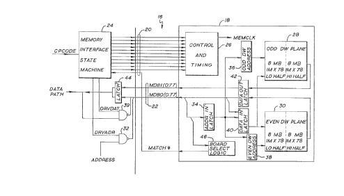
Referring first to Fig. 1 there is shown in block
diagram form a portion of an information processing
system 10. System 10 includes a system bus 12 which
couples together a number of bus connections including
a memory control unit (MCU) 14. Other bus connections,
such as a CPU (not shown) provide data to the MCU 14 to
be written to memory and also receive data read from
memory. Coupled to MCU 14 via a memory bus (MEMBUS) 16
are one or more memory units (MUs) 18. For example, in
the illustrated embodiment up to eight MUs 18 (MUO-MU7)-
can be coupled to the MCU 14 via the MEMBUS 16. MEMBUS
16 can be seen to comprise two groups of signal lines
including a control bus 20 and a data/address bus 22.
Referring to Fig. 2a there is shown the memory bus 16
in greater detail. The control bus 20 can be seen to
comprise a plurality of signal'lines which are sourced
by, for example, a memory interface state machine 24 on
the MCU 14. The memory interface state machine 24 is
responsive to a memory access type opcode which is
generated by a bus connection and which is sent over
the system bus 12 to the MCU 14. The opcode defines a
particular type of memory access such as a double-ward
read, a quad-word read, or a word or double-word write.
The memory interface state machine 24 decodes the
opcode and provides the necessary sequence of control
signals to the MUs 18. A control and timing logic
block 26 on the MU 18 receives the control bus 20
signals and, in synchronism with a memory clock
(MEMCLK), generates a plurality of internal timing
2Q48669
9
signals for the MU 18. The MU 18 can be further seen
to include an odd double-word memory plane 28 and an
even double-word memory plane 30. Planes 28 and 30 are
each comprised of a plurality of memory devices which
are preferably DRAMS. In the illustrated embodiment
each of the planes 28 and 30 is differentiated into an
upper and a lower half, each half having eight
megabytes of storage organized as one megabyte by 78
bits. Sixty-four of the bits comprise a data
double-word and the remaining 14 bits are error
detection and correction (ECC) syndrome bits. A memory
address is provided to the planes 28 and 30 from the
MCU 14 via a memory address driver 32 which is.
controlled by a drive address (DRVADR) signal generated
by the memory interface state machine 24. It should be
noted that in this embodiment of the invention that the
address bits are time multiplexed with a portion of the
data bus 22. The address is latched in the MU 18 by an
address input latch 34 and is provided to two address
logic blocks 36 and 38, block 36 being associated with
the odd double-word plane 28 and block 38 being
associated with the even double-word plane 30. At a
subsequent time in the memory access cycle the memory
interface state machine 24, for a write type of memory
access, generates a drive data signal (DRVDAT) which
drives, via a driver 39, the contents of an interl
data path to the MEMBUS data/address bus 22. It shd~ld
be noted that for the illustrated embodiment of the
invention that a single write cycle may be up to 64
data bits (double-word) in width (plus ECC syndrome
bits) while a single read access cycle may be up to 128
bits (quad-word) in width. During a write type of
access the data driven to MDBO <00:77> is received by a
' 10
data input latch 40 and is provided therefrom to one of
the planes 28 and 30 while a write strobe (WSTB) signal
is gated to the proper plane for writing. During a
memory read type of access the data outputs from the
planes 28 and/or 30 are provided to a data output latch
42 which drives the data/address bus 22. The data is
received by a latch 44 on the MCU 14 and is provided
therefrom to the internal MCU 14 data path. The MU 18
also includes a unit select logic block 46 which
decodes a portion of the address input to determine
whether a particular MU 18 is selected by (matches) the
provided address. The unit select logic block 46
returns a signal MATCH* to the MCU 14 if a MATCH.
condition is detected.
Fig. 2b illustrates the MU 18 in use with a MCU 14'
which employs a single 78-bit data/address bus 22.
Thus, for this type of MCU 14' both the write and the
read data paths are of equal width. In accordance with
one aspect of the invention the MU 18 includes an
additional data latch 48 which is employed to multiplex
the data output of the odd double-word plane 28 onto
the MDBO (00:77) bus 22. The operation of latch 48 is
controlled by the control and timing block 26, as are
the other latches and logic previously described, which
in turn is responsive to particular ones of the control
bus 20 signals as will be described.
It can be seen that the MU 18 provides either a fist
data bus width or a second data bus width which is
twice that of the first width. Thus, the MU 18 can be
employed with at least the two types of MCU 14 and 14'
2008669
without requiring circuit changes to be made to the l~t~
18.
Referring now to the block diagrams of Figs.2c, 3a, 3b and
3c there is shown the MU 18 in greater detail.
Specifically there is shown in Fig. 2c the control and
timing block 26 in greater detail and in Figs. 3a, 3b and
3c the internal address and data paths and also the
board address match logic. In Fig. 3a it can be seen
the MD80 <00:77> bus is coupled to the address input
latch 34 which can further be seen is comprised of a
buffer 34a and latch 34b. During the address portion
of the memory bus cycle 28 bits of address are applied.
on the MD80 signal linen and are latched by latch 34b
for application to the even double-word address logic
38 and the odd double-word address logic 36. The odd
double-word address logic 36 can be seen to include a
counter 36a and a row and column select multiplexer
36b. The even double-word address logic 38 is
comprised of an adder 38a, a counter 38b and a row and
column select logic 38c. Counters 36a and 38b are each
an eight-bit counter which are preloaded with eight
bits of the latched column address (LA(20-27)).
Counters 36a and 38b each have an input ( INCADDR) for
incrementing the counter value by a value of one for
accessing consecutive double-words from their
respective memory planes. Ths adder 38 is provided for
initially prsincrementing tho evon double-word column
address by a value of one when are. ADp signal, LA 28 w '.
1, is asserted. This preincrsment is accomplished when
a starting memory address bogies from the odd
double-word plane. It should be noted that two bits of
the latched address (LA28 and LA29j are not applied
,,~-~, i
12 2008669
directly to the memories. Bit 29 is applied to the
control block 26 and selects within a memory plane the
even or odd word while bit 28 is employed for selecting
either the even or the odd memory planes 28 and 30 for
access.
By example, and assuming that an initial address refers
to the even word plane, LA<26-29> may equal 0100
2'
This results in the least significant four bits of each
of the counters 36a and 38b being loaded with a value
of 0001~2~, it being remembered that bits LA 28 and 29
are not applied to the counters. Thus, both planes 28
and 30 are provided with an address having LSBs of-
0001~2~. If. the access is a multiple quad-word read
access, both planes retrieve data from the provided
address. After a first memory read access the counters
36a and 38b are both incremented by the assertion of
INCADDR such that both have a value of 0010~2~ for
accessing the next consecutive double-word.
However, if LA28 of the initial address points to the
odd double-word plane 28, such as an address of
0110~2~, both counters will again have an initial value
of 0001~2~. In this case of starting an access from
the odd double-word plane, the adder 38a first adds a
one to the even memory plane 30 column address befpre
the address is stored in counter 38b such that the even
double-word plane counter 38b does not fall behind the
odd plane counter 36a. That is, the odd double-word
plane is accessed at address 0001~2~ while the even
double-word plane is initially accessed at address
0010~2~. After incrementing both counters 36a and 38b
the next odd plane address from counter 36a is 0010
C
13 zoossss
while the next even plane address from counter 38b is
0011 ~ 2 ~ .
The multiplexers 36b and 38c each apply two sets of il
bits of address to the DRAM double-word memory planes
28 and 30 which, in conjunction with the appropriate
RAS* and CAS* signals, are strobed into the memories
for selecting a particular address location. The
assertion of the RAM COL* signal switches the output of
multiplexers 36b and 38c from the row address to the
column address provided by the counters 36a and 38b,
respectively. It should be realized that ten of these
eleven address bits are strobed directly into the one-
megabyte DRAMS and that in other embodiments of the
invention that more or less than this number of bits
are provided depending on the density of the individual
memory devices. For example, if four megbyte DRAMs are
employed all eleven of the address bits are used.
Data input latch 40 is employed during memory write
cycles and is a 64 data bit, plus 14 ECC syndrome bit
width latch, the outputs of which are applied to the
data input terminals of the memory devices of the two
memory planes 28 and 30.
Each of the double-word memory planes 28 and 30 has a
data output latch associated , herewith, namely ~:
78-bit latches L4 42a and L6 42b. Latches,L4 42a and
L6 42b are employed when the MU 18 is utilized with the
MCU 14 of Fig. 2a for simultaneously providing up to
128 bits, or one quad-word of data, for memory read
cycles. Each of the latches L4 42a and L6 42b has an
associated 78-bit output driver 50 and 52,
' 77215-1
14 2008669
respectively, coupled to an output thereof for driving the MDBO
and MDB1 buses, respectively.
In accordance with one aspect of the invention the
odd double-word memory plane 28 further has the 78-bit latch L5
48 coupled to its output, the latch 48 having an output coupled
to the input of the even double-word memory plane driver 50.
Thus, for those types of applications which employ a 64 bit, as
opposed to a 128 bit, memory data bus the latch 48 is utilized
to multiplex the output of the odd double-word memory plane 28
l0 on to the MDBO<00:77> bus.
The MU 18 further includes a memory logic array (MLA)
54 which is utilized to determine if a particular bus address
selects the MU 18 for a read or write cycle. A base address
input is compared to a portion of the address from buffer 34a.
If the address is determined to be within a range of addresses
which correspond to a particular MU 18 an output of a
comparator 56 asserts the MATCH* signal which is provided on
the memory bus 16 to the MU 14. The MLA 54 further functions
to provide a base address output to a next consecutive MU 18 in
a manner which is disclosed in U.S. Patent 5,307,469 which
issued on April 26, 1994.
Fig. 4 shows in greater detail the memory control bus
20 of Fig. 2a and Fig. 2b. The function of the various signals
shown in Fig. 4 are better understood by also referring to the
timing diagrams of Figs. 5-12 which show a variety of memory
access types.
i
15 zoo8sss
The MEMCLOCK* signal is provided from the MCU 14 to the
MU 18 and establishes a reference clock signal for the
MU 18. The CLOSE* signal captures and latches the
address appearing on MDBO<02:31> at the beginning of a
memory operation. As can be seen in Fig. 5, the CLOSE
signal is asserted when the memory address is set up on
MDBO at the beginning of a memory access cycle. CLOSE
remains asserted until the end of the memory access
cycle. DTOUT* and DTIN* are provided from the MCU 14
and convey a four bit code to the MU 18. The four bit
code provided by the DTOUT* and DTIN* signals are
employed during read and write operations and is used
by the MU 18 to enable the MU 18 buffers and other.
circuitry for writing to the MU 18 or for reading from
the MU 18. Table 1 illustrates the use of DTOUT* and
DTIN* in conjunction with other signals.
,....
16 2oo~ss9
DESC RIPTIONF DTOUT* AND DTIN*
O
DTOUT* DTIN* QDBS* BDWD* LA28
0 X 0 1 0 Enables latch ~ driver
outputs (42a & 50) to send
data to MCU for memory
reads
0 X 0 1 1 Enables latch ~ driver
outputs
(42b ~ 52) to send read
data
to MCU for memory reads
0 X 0 0 X Enables latch & driver
outputs
'(42a ~ 50 b 42b & 52)
to send
read data to MCU for memory
reads
0 0 1 X X Enables latch 6 driver
outputs (48 ~ 50) to send
read
data to MCU for memory
reads
0 1 1 X X Enables latch ~ driver
outputs
(42a & 50) to send read
data
to MCU for memory reads
1 0 X X X Enables buffer & latch
outputs (34a ~ 40) to drive
data into MU array for
writes
1 1 X X X No buffer or latch outputs
enabled
i
i l~ zoo8sss
The row address strobe (RAS*) signal is generated by
the MCU 14 and is provided via the control and timing
block 26 to the memory devices on the MU 18 to strobe
in the row address provided from the multiplexers 36b
and 38c. The column address strobe (CAS*) is generated
by the MU 18 for both read and write access cycles. It
should be noted that if the memory unit has static
column type DRAMS that CAS* remains asserted during
multiple memory access cycles. A write strobe (WRSTB*)
is generated by the MCU 14 for write-type access cycles
and is provided, as can - be seen in Fig. 8,
substantially coincidentally with the provision of
write data~on the memory bus 16.
The control bus 20 includes a BWD* signal and a BDWD*
signal. As can be seen in Figs. 5-12, the BWD* signal
is utilized for all memory accesses of a double-word or
greater in width. The BDWD* signal is used for all
memory accesses which are a quad-word in width. BDW*
and BDWD* control, via the control and timing block 26,
which of the memory planes 28 and 30 receive RAS*, CAS*
and WRSTRB*. For a byte or word write cycle (Figs. 8
and 9) neither BDW* or BDWD* is generated, the memory
plane section being accomplished by LA<29>. For a
double-word operation LA<29> is ignored and BDW* and
LA<28> control the memory plane selection. For an-
operation greater than a double-word, LA 29 and LA 28
are ignored and BWD* and BDWD* control memory plane
selection. For this case LA 28 controls the proper
sequencing of the planes.
18 2oosss9
A refresh (RFRSH*) signal is periodically generated by
the MCU 14 in order to initiate a refresh cycle on the
MU 18. As can be seen in Fig. 11, the refresh cycle is
performed as a read operation, having both RAS* and
CAS* asserted, which enables the MCU 14 to read the
data at the refresh location and to perform error
"sniffing" and correction if necessary. In Fig. 12 it
can be seen that the refresh cycle indicated a bit in
error and that corrected data is written back to the MU
18 during the time that the WSTRB* signal is asserted.
The MATCHED* signal is returned to the MCU 14 only by
the MU 18 which generates a matched condition with the_
MCU 14 provided address. Furthermore, a STATMATCH*
signal is provided back the MCU 14 simultaneously with
the provision of the MATCHED* signal only for those MU
18s which employ static column DRAMS. The STATMATCH*
signal can be utilized by the MCU 14 to modify its
internal timing in that the STATMATCH* signal being
asserted generally indicates that a faster memory
access is possible.
The AHCMATCH* signal is output from the matched MU to
the MCU 14: the assertion of AHCMATCH* being caused by
the generation of MATCHED* and also a MU jumper or
switch which indicates that DRAMS having a specified
speed are installed. AHCMATCH* is a status signal, to
the MCU 14 which indicates that the MU is adding o~te
half of a MEMCLK cycle to the memory access to
accommodate the timing requirements of the DRAMS. For
example, if faster access DRAMs are installed the
jumper may not be set and AHCMATCH* is therefore not
asserted.
i
2oosss9
19
As was previously discussed, page mode DRAMs are
characterized as requiring multiple assertion of CAS*
in order to accomplish consecutive memory accesses. In
accordance with one aspect of the invention the NEXT*
signal is utilized for page mode DRAMS in order to
cause successive assertions of the CAS* signal. It
should be remembered that the counters 38b and 36a can
also be incremented by NEXT* between accesses in order
to increment the column address. Therefore, the
assertion of the NEXT* signal is employed for multiple
read and write type of accesses for page mode DRAMs as
well as for static-column. DRAMS. However, the
assertion of NEXT*, for static column DRAMs, increments-
the address but does not affect CAS*.
The Next Enable (NEXTENA*) signal is employed, when
asserted, to enable the gating of the NEXT* signal onto
the MU 18. The NEXTENA* signal can be hard wired on
the control bus 20 to either an enabling or a disabling
logic state. The assertion of NEXTENA* indicates that
the MU 18 is coupled to an MCU which generates the
signal NEXT* to perform multiple memory accesses.
Further in accordance with the invention there is
provided a quad data bus (QDBS*) signal which specifies
to the MU 18 whether the MEMBUS 16 is a double-word (,~4,.
bit) or a quad-word (128 bit) type bus. As with the
NEXTENA* signal the QDBS* signal can be tied to a logic
signal on the MEMBUS 16. When the QDBS* signal is
asserted the MU 18 is notified that it is installed in
a quad-word bus type of system. When the QDBS* signal
is not asserted the MU 18 is notified that it is
installed in a double-word bus type of system and that
,'~ (_
2oosss9
latch L5 48 is required to multiplex the odd
double-word plane 28 output onto the MDBO bus.
As can be seen in Fig. 2c the NEXTENA* signal enables
5 the generation of an ENABLECAS* signal via gate 62, F/F
64 and gate 66. The output of F/F 64 is a registered
NEXT* (RNEXT*) signal. The ENABLECAS* signal is
asserted when NEXT* is asserted by the MCU 14 in
conjunction with the NEXTENA* signal and also when the
10 MU 18 provides a signal STATCOL which indicates that
static column DRAMS are not installed. The ENABLECAS*
signal is provided to a Memory Array Control (MAC)
block 68 for enabling the assertion of certain CAS<0:7>
signals to the memory planes 28 and 30. If STATCOL
15 indicates that static column DRAMS are installed
ENABLECAS* is generated and the transitions of the
address inputs to the DRAMs, provided from counters 36a
and 38b via multiplexers 36b and 38c, provide the
required DRAM activation to access a next column
20 address. The assertion of RAS* by the MCU 14 further
initiates the assertion of certain ones of the
RAS<0:7>* memory strobes which initiate the memory
access cycle. At the end of a particular RAS* cycle a
signal RASEND is asserted by MAC 68 to gate 70 which,
regardless of the state of ENABLECAS*, generates the
INCADDR signal to counters 36a and 38b. If NEXTENA* is
asserted the INCADDR signal is generated from RNXT*.
- Figs. 13a, 13b and 13c are timing diagrams which
illustrate the operation of these signal lines in
different configurations of systems. Specifically,
Fig. 13a shows a double-word width data bus system
having page mode DRAMs and a maximum operation size of
an octal-word read. Fig. 13b illustrates a quad-word
i l
a 1 X008669
width data bus system having static column DRAMs. Fig.
13c illustrates a quad-word width data bus system
having page mode DRAMs. In these three Figs. 13a-13c
it should be noted that the terminal rising edge of the
increment address (INCADDR) signal is a don't care
state in that the operation has already ended.
MAC 68 includes a number of Control Bus 20 inputs
including WRST*, BWD*, BDWD*, DTIN* and DTOUT*. The
state of these signals is decoded by the MAC 68 for
generating the required ones of the memory strobe
signals. A portion of the MAC.68 is a Latch Control 72
which decodes certain of the input signals for.
generating various latch controlling outputs, including
L4CONT, LSCONT and L6CONT. By example, if QDBS* is
asserted then LSCONT is not generated, QDBS* indicating
that the MU 18 is installed in a quad-word wide MEMBUS
16 system. Conversely, if QDBS* is not asserted then
LSCONT is generated for multiplexing the odd
double-word memory plane output to the even double-word
bus, namely MDBO<00:77>. The MAC 68 also controls the
generation of the ADD signal to adder 38a to initially
add a one to the even double-word counter 38b as
previously described.
It can be appreciated that inasmuch as counters 36a and
38b are both eight bit counters that the operation of
Control Bus 20 in conjunction with Control and Timing
block 26 enables up to 128 consecutive quad-word read
cycles or up to 256 consecutive double-word write
cycles. These consecutive read or write accesses are
accomplished by providing the initial address and
,i
22 2oosss9
thereafter repetitively asserting the NEXT* signal from
the MCU 14:
Referring to Fig. 5 there is shown the operation of the
Control Bus 20 and certain MU 18 and MCU 14 signals for
a double-word read cycle. The MEMCLOCK signal provides
a reference clock, cycles of which are shown numbered
consecutively. At the beginning of the read cycle the
address from MCU 14 is stable at the rising edge of
MEMCLOCK 2 and the CLOSE* and RAS* signals are
asserted. The BWD* signal is also asserted for
indicating that a double-word.operation is in progress.
A row address is provided by the appropriate.
multiplexes 36b or 38c and at rising edge of MEMCLOCR3
the row address is strobed into the DRAMS by the RAM
RAS* signal. The multiplexes thereafter switches to the
column address provided from the associated counter 36a
or 38b and RAM CAS* is generated at MEMCLOCK4 for
strobing into the addressed DRAMs the column address.
At MEMCLOCK5 the MCU 14 asserts DTOUT* to enable output
drivers etc., thereby enabling the MU 18 output data
path, including the appropriate data latch. Data read
from the addressed memory plane is driven to the
appropriate MDB bus 22. During MEMCLOCK6 the MCU 14
latches the data and at the end of MEMCLOCK6 CLOSE* is
deasserted, thereby terminating the MCU 14 access.
Fig. 6 illustrates a quad-word read cycle wherein the
QD bus is used, this cycle being similar in operation
to the double-word read of Fig. 5. However, both the
MDBO and MD81 buses are employed. Also, it can be seen
that the DBwD* signal is asserted coincidentally with
BWD* for indicating that both double-word memory planes
2008669
23
28 and 30 are being accessed. The diagram of Fig. 6
illustrates the quad-word MEMBUS 16 configuration, the
QDBS* signal (not shown) being asserted from the
backplane. If the double-word MEMBUS 16' 'of Fig. 2b is
employed the latch L5 48 is employed to provide the odd
memory plane double-word to MDBO in the MEMCIACRB. Of
course, the deassertion of the CLOSE* is delayed until
the end of MEMCLOCK 8 in order to accommodate the
additional time required to transfer the odd memory
plane double-word to the MCU 14. Fig. 6a illustrates
an octal-word read cycle and Fig. 6b a quad-word read
for the double-word width bus.case. The RCLOSE* signal
is a registered CLOSE* signal.
Fig. 7 illustrates two consecutive quad-word read
operations, it being realized that up to 128 quad-word
reads may be accomplished in such manner. The memory
access proceeds up to MEMCLOCK5 in a manner as
previously described. At MEMCLOCK5 the NEXT* signal is
asserted to indicate that a second quad-word read cycle
is desired. The rising edge of NEXT* at MEMCLOCK6
causes the generation of the INCADDR signal thereby
incrementing the column address counters 36a and 38b.
If static column type DRAMS are installed RAM CAS*
remains asserted and the change of state of the column
address initiates the next DRAM access cycle. If page
mode type DRAMs are installed RAM CAS* is deasserted,
as indicated in dashed outline, for one MEMCLOCK cycle
after which RAM CAS* is once more asserted to initiate
the second DRAM access. DTOUT* is asserted a second
time in order to retrieve the second quad-word of data.
If more than two quad-words of data are required each
2oosss9
24
quad-word is accessed by the assertion of NEXT* with an
assertion of DTOUT*.
Fig. 8 illustrates a byte write operation. This type of
write operation is achieved by initially performing a
word or a double-word read of the memory plane having
the byte to be written, merging within the MCU 14 the
byte into the word or double-word and writing back the
merged word or double-word to the memory plane. This
portion of the cycle is accomplished from MEMCLOCK1 to
MEMCLOCK7. At MEMCLOCK7 DTIN* is asserted and at
MEMCLOCK8 WRSTRB* is asserted. The double-word
containing the newly merged byte of data is also driven.
to MDBO<00:77> at MEMCLOCK8. It can be noted that RAM
CAS* remains asserted throughout this read-modify-write
type of access.
Fig. 9 illustrates a word or a double-word type of
write cycle. BWD* is not asserted for a word write
cycle but is asserted, as shown in dashed outline, at
MEMCLOCK2 for the double-word case.
Fig. 10 illustrates a consecutive double-word write
access. A first double-word is driven to MDBO<00:77>
during MEMCLOCK4 in conjunction with WRSTB*. This first
double-word is stored in either the odd or even memory
plane depending on the state of the address (LA 28)
driven during MEMCLOCK2 and MEMCLOCK3. A second
double-word is driven at MEMCLOCK6 along with WRSTRB*
and the second double-word is stored in the memory
plane not previously written. NEXT* is asserted at
MEMCLOCK7, the rising edge of which at MEMCLOCK8 causes
the column address to increment via counters 36a and
,,..,~
25 2UO8669
38b. The third and fourth double-words are driven,
along with an associated WRSTB*, during MEMCLOCKB-12
for storage within the memory planes. Both BWD* and
BDWD* are asserted at MEMCLOCK2 and DTIN* is asserted
at MEMCLOCK3. If an additional double-word write access
were required NEXT* would be reasserted at MEMCLOCKil
with CLOSE*, RAS* and DTIN* remaining asserted.
Fig. 11 illustrates a refresh operation which is
periodically initiated by the MCU 14 for refreshing the
DRAMs. The refresh operation is performed as a word or
double-word read operation similar to that of Fig. 5.
The word or double-word of data, including ECC syndrome.
bits, which is read from the refreshed location is
processed by error detection and correction circuitry
within the MCU 18 to detect and correct single bit
errors or to detect multiple bit errors. During a
refresh cycle the RFRSIi* signal is asserted by the MCU
14 in conjunction with CLOSE*, RAS* and BWD*. Fig. il
shows the case where no errors are detected.
Fig. 12 illustrates a refresh operation wherein a bit
of the word or double-word is found to be in error. As
can be readily seen, the operation of this refresh
cycle during MEMCLOCK1-8 is identical to that of Fig.
11. In that a bit is in error the error is corrected by
the MCU 14 and a word or double-word write cycle is
initiated at MEMCLOCK8 in order to write the corrected _
word or double=word back into the memory location from ~ .
which it was read. This MCU 14 initiated write cycle
can be seen to be identical to that of Fig. 9 with BWD*
asserted.
2008669
26
While the invention has been particularly shown and
described with respect to a preferred embodiment
thereof, it will be understood by those skilled in the
art that changes in form and details may be made
therein without departing from the scope and spirit of
the invention.