Note: Descriptions are shown in the official language in which they were submitted.
200~903
- 1 -
DUAL RAIL DILATED SWlTCHING NETWORKS
Ba.l~ ' of the Invention
This invention relates to optical switching networks and, more
S~ to optical switching network r ~'~ -~ `. that rcduce crosstallc noise
5 through judicious routing of signals.
Wideband optical signals can be switched with electronic control using
Clc~,LIw~)Lic waveguide couplers using TiLiNbO3 ~va~ S id~,~ on a planar LiNbO3
crystal. The basic switching element is a coupler with two active inputs and twoactive outputs. Depending on the amount of voltage at the junction of the two
0 ~'VAV~ 5 hl~ which carry the two input signals, the two inputs can be coupled to
either of the two outputs. Several all ' c~ have been proposed to construct an
NxN switch with the 2x2 directional coupler as the basic ~ ~ These
a~ are essentially analogs of similar A~ for electronic switching
and illt~,l. networks. However, due to the difference in . l IAI ~ of
15 the electronic and optical switching elements, p, ~ ~ of the optical
;t~,Luu~., is significantly different.
Specifically, ~ of signals in optical systems is difficult. This
difficultv leads to the desirc to reduce losses and eliminate noise sources so that the
need for ~ ;.... can be ~iimir~i~h~l In light of this desire, some al~llit~ ul"~20 that are useful when realized with electronics are less favored for optical n-Ali7~ti~-n~
Tho attenuation of light passing through a waveguide optical coupler
switch has several Cullll~ (a) fiber-to-switch and switch-to-fiber coupling loss,
(b) y~ a~aLiul~ Ioss in the medium, (c) loss at waveguide bends, ând (d) loss at the
couplers on the substrate. Often, the last factor ~ ' and, therefore, a
25 substantial part of the attenuation in a switch fabric is directly ~lupolLi-~ lal to the
number of couplers that the optical path passes through.
Optical crosstallc results when two signals interact with each other.
There are two primary ways in which signals flowing in optical paths can interact in
a planar substrate. First, the channels (wa~,guid~,~) carrying the signals could cross
30 each other in order to imbue a particular topology and the interaction occurs in the
llc;r-hbu,l.~,od of the crossover. Secondly, two paths sharing a switching element
experience some undesired coupling from one paLh to the other. We call the former
path crossover crosstalk, and the latter swi~ch crossover crosstalk The easiest way
to reduce palh crossover crosstallc is to reduce the size of the n~i~hh,~rh~ 1 within
35 which the interaction occurs. This can be a~ c ~ " ~ by keeping the i.lt~
angles above a certain minimum amount. A more difficult approach is to make the
.... .. . ... _ , . _ .. _ _ . ,
-2- 2008903
interaction nc;ghlvol l.ood precisely long enough to couple the signal entirely from one
path to the other and back with path crossova crosstalk reduced to a negligible level, swi~ch
crossovas remaim as the major source of crosstalk in optical switching networks constructed
out of clc~lluu~J~ic waveguide couplers.
The effort to reduce crosstalk is hence directed at the switch design, at the
number of switches that a particular architecture requires in the optical path, and at the
signal flow patterns within the network.
In the IEEE Transacrions on ~ , Vol. COM-35, No. 12, December,
1987, we published an article title "Dilated networks for Photonic Switching". The article
presents a number of networks wherein the third approach to reducing crosstalk is
diselosed. We eall this the dilated networks approaeh. Speeially, we disclosed a design for
the Benes network that, while ~ v the Iciallall~CdblC non-blocking . l, " ,,. I rl ;~1 i
of the network insures that no 2x2 switch in the network has optical signals applied
COl~ Lly to both its inputs. We also mentioned that a CUllv~JUlldillg design for the
Omega network is possible.
What we have not described, however, is a method for modifying the
structure of any given network to create a corresponding network that is dilated.
Summarv ûf the Invention
~n acculda.l~6 with one aspect of the invention there is provided a network
for routing signals: . v a plurality of routing elements, each comprising a first pair
of input leads, a second pair of input leads, a first pair of output leads amd a second paid
oE output leads; and an illLtl. u..lle~.liu~ wherein said first pair of input leads
of one of said routing elements is connected to a pair of output leads of another one of
said routing elements, and said second pair of input leads of said one of said routing
25 elements is connected to a pair of output leads of stiU another one of said routing
elements.
In d~ ~ uldallce with another aspect of the invention there is provided a
method for ereatirlg an altered version of a given network that employs single rail 2x2
switches and includes single rail input signals and smgle rail output signals, comprising the
30 steps of: employing a dual rail switch in said altered version of a given network in place of
a smgle rail switch in said given network, said dual rail switch comprising two input pairs
-2a- 20~8903
of leads and two output paid oE leads; employing a pair oE links in said altered version oE a
given network in place of a single link in said dven network; and employing a combiner
stage as the ultimate stage oE said altered version oE a given network to combine pairs oE
output signals in a ~ ' stage of said altered version oE a given network to form5 single rail output signals or said altered version of a dven network that parallel said single
rail output signals of said dven network.
In acc.,.Jdl.~ c with the principles oE our invention, our method can be
applied to any dven switching network design that employs 2x2 switches the method yields
a l;u~ u~iJillg dilated switching network design. The dilated switcbing network diEEers
10 Erom the oridnal switching network in only two ,lldla~ Leli~i~. First our dilated network
guarantees that at no point in the network can two active signals ~:u~ ly appear at
the two inputs (or two outputs) of a 2x2 switch. This eliminates crosstalk. F~ tin~
crosstalk extracts a price, however, and that price is the second difEerence between the
networks. Specifically, the number oE 2x2 switches in our dilated network (a
15 Ull~ ollJillg connection links) is ~ l U~ dL.,l,~ twice the number oE switches in the
oridnal network
Our method calls Eor three steps: first, replacing each 2x2 switch with a dual
rail switch that contains a pair oE 2x2 switches; second, replacing each link that connects
an output lead oE one switch to an input lead oE another switch with a pair oE links that
20 connect a pair oE output links oE one dual rail switch to a pair oE input links oE another
dual rail switch; and third, combining pairs of output leads at the last stage oE the network
tp ~olrd :Ing:e O~ltpllt lcads
2~0~9Q3
- 3 -
Brief Description of the Drawin~ _
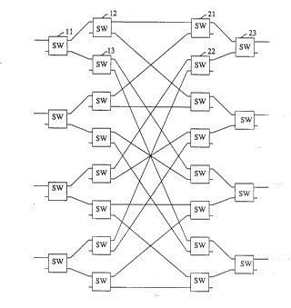
FIG. 1 illustrates a crossbar switch design using 2x2 switches;
FIG. 2 presents our dual rail 2x2 switch;
FIG. 3 presents a slight variation on the dual rail switch of F~G. 2;
FIG. 4 shows a dilated switching network realization for the Omega
network with 8 inputs and outputs;
FIG, 5 shows an undilated and a dilated realization of a diamond alray;
FIG. 6 shows an undilated and a dilated realization of a Banyan
network; and
FIG. 7 shows an undilated and a dilated realization of a mesh-connected
crossbar.
Detailed Description
The only condition on deriving a dilated version of a network is that no
switch should c~ 'y carry two active signals, regardless of the p~
15 that is being realized. If every switch in the network has only one of its inputs
connected, or only one of its outputs connected, then the network is dilated, bydefinition. We call such an ;...~ a "fan-in/fan-out" ;, .~ II A
fan-in/fan-out l l of a four line crossbar is shown in FIG. 1. ~lements
11, 12, and 13, for example, are one-to-two splitter elements. Though structurally
20 they are 2x2 switches, each accepts an optical signal at only one input, As
ihlt~ .~, they combine to develop four outputs. At any instant, no more than
one of the four outputs can carry an optical signal. The four outputs of elements 12
and 13 are connected to two-to-one combiner elements such as element 21.
Structurally, the combiner elements are also 2x2 switches, but they are arranged with
25 the I ' " 3 that the control signals will insure that whatever optical signal is
received at a combiner's input, it will be delivered to the combiner's selected output.
The ~isa.lv ~ inherent in the fan-in/fan-out dilation of FIG. 1 is, of
course, the large number of switches that is required. For an NxN crossbar, for
example, the number of required 2x2 switches is 2N(N- 1). This number is not the30 minimum number of switches with which an NxN network can be; ~ .1 As
shown in our ar~ ' article by way of a counter example, we created a
Benes network with a number of 2x2 switches on the order of Nlog2N.
Neither the FIG. 1 a~ ulc nor the Benes a~,lf. ~ e are
~a~i~ra~,~uly for all A~ ..c What would be useful, and what the instant
35 invention offers, is the ability for artisans to select a particular network topology
based on their specific set of system ~ .n~ ,e l~l": c, . . ~ and then perrnit the
.... ... .... .... .. .... .. . _ . ... ..... _ .. . _ ... _ _ .. _ . _ _ _ _ . . ..
2008903
- 4 -
doveloped network to be converted to a dilated realization. In accordance with the
principles of our invention, a canonical ;~ ,l "- ~ 11 approach can be employed
to achieve a dilated version of any ,.~r. . ~ ;fm network uo.~ u~,t~;l from 2x2
switches.
Under the condition that no switching element carry at any instant an
optical signal in both its input ports and/or both its output ports, the simplest
switching function of two inputs is shown in FIG. 2. That is, in accordance with the
principles of our invention, the FIG. 2 circuit is a direct substitute of a u~lv.,.lliulldl
2x2 switch. Just as the Cul~v~ lal 2x2 switch has a "pass-thru" state and a
10 "crossover" state, so does the circuit of FIG 2. We call the Al I A.l~, .11. ~1 of FTG. 2 a
dual rail switch.
In FIG. 2, each of the two inputs signals is assumed to comprise two
rails. One rail carries an active signal, while the other one does not. Each input pair
(the two rails) is connected to a different 2x2 switch. In FIG. 2, one input pair is
applied to input leads 31 and 32 of switch 30, while the other input pair is applied to
input leds 33 and 34 of switch 4Q As drawn, the active inputs (marked by " I ") are at
leads 31 and 33. Given that at most one of the two input leads of a 2x2 switch carry
a signal, the switching state of switches 30 and 40 is well defined. Specifically,
when the acive signals are at the same spatial sense (i.e., leads 31 and 33 active or
leads 32 and 34 active), then the states of switches 30 and 40 are reversed from one
another. Conversely, when the active signals are at a crossed spatial sense (leads 31
and 34 active or leads 32 and 33 active) then the states of switches 30 and 40 are
identical (i.e., both "crossover", or both "pass-thru"). A more detailed
of the states of switches 30 and 40 is presented in the table below.
~OOt~903
- 5 -
input input connection switch switch
31 32 33 34 type 30 40
0 1 0 pass-thru pass-thru pass-thru
0 1 0 crossover crossover crossover
5 1 0 0 1 pass-thru pass-thru crossover
0 0 1 crossover crossover pass-thru
0 1 1 0 pass-thru crossover pass-thru
0 1 1 0 crossover pass-thru crossover
0 1 0 I pass-thru crossover crossover
10 0 1 0 I crossover pass-thru pass-thru
FIG. 3 presents a variation on the dual rail switch of FIG. 2~ Its only
difference is in the spatial sense that the outputs exhibit for different spatial senses of
the input. Specifically, the FlG. 3 dual rail switch forces the two output pairs to have
a like spatial sense. Either the top rail of both output pairs is active, or the bottom
15 rail of both output parrs is active.
In accordance with the principles of our invention, any network
topology or al~.l it~ulc that employs 2x2 switches can be realized in a dilated forrn
by (1) replacing the single rail 2x2 switches of the network with the dual rail
switches of FIG. 2 (or FIG. 3), (2) .,U.~ ,Lil.g the dual rail switches with pairs
20 of lines in a manner that essentially replaces the single line . : of the
undilated network with line pairs, and (3) insuring with d~ n control signals
as described above that each pair of lines has, at most, one lead that carries active
signal i..r~ lio-l. The latter, of course, is an operational ~ rather than a
structural one.
FIG. 4 illustrates the use of our approach in connection with the network
known as the omega network (with the input shuff~e deleted for sake of sirnplicity).
The dual rail switches are marked by dashed blocks 41-52. In blocks 41-44 only one
input of each input pair is connected to the incoming signal. The other inputs are
simply not used. This insures the first of the ICI~,U', Cl~ for blocks 41-44; that of
30 no more than one active input at each pair of inputs to each 2x2 coupler within the
dual rail switch. The IC~Iuil~ that no pair of outputs should contain a signal in
both of the output leads is satisfied by a judicious application of control signals to
the couplers within the dual rail switches, as described above. The final stage of the
network, which in the case of FIG. 4 is dual rail switches 49-52, the output pairs
35 contain an active signal in only one of the leads. Each of the output pairs should be
combined to a single output lead and, accordingly, FIG. 4 includes combiners 53-60
200~39~)3
- 6 -
which serve this function. It may be noted that switches 41~4 could be CU~ u~,~Gd
from switches that are simpler than the dual rail switch of FIG. 2. Conversely, the
combiner switches 53-60 can be realized with tho dual rail switches used elsewhere
in the network. It is simply a designer's choice.
S FIG. 4 dopicts a very small network; only 8 inputs and outputs. Because
of its small size, the . t;vi~y pattem perhaps is not obvious from the figure itself
but, of course, the omega network is well known in the a}t. N.,~ ;.cl~, for the
sake of ~ , the description below presents the Cullll~livi~y pattern of the
omega network in "closed form". The ~ , G developed for the omega
10 network is also used in connection with other networks that are described infra.
The omega network is one of a class of networks that require log2N
stages of switching elements for an N input and N output network. The ~UlI.._~,IiVi~y
of the switching elements can be described by fl~c~ in~ each stage with a variable,
such as i, ranging from 0 to (log2N)-l. Each input and output lead of a stage is15 labeled from 0 to N ~starting, for example, from the top of the figure), and the label
is expressed in binary form. A specific input link is thus identified by
I(p,_lp}2pl_3 Pj P2PlPo)i.
where I = log2N, i is the stage number and I designates the link as an input link.
Similarly, a specific output link is identified by
20 (PI-IP~2Pl-3' Pj P2PIPo)i.
where O designates the link as an output link.
The: 'vi~y pattem for the undilated omega network is
O(PI-IPI-2P~3 ' Pj ' ' ' P2PIPo)i~I(P}2PI-3 ' ' Pj ' ' ' P2PlPoPI-I)i+l.
where ~ designates a connection between the links identified on the two sides of the
25 arrow. Note that it merely is a circular left shift.
The dilated omega network of our invention has twice as many links
between the switching stages as there are in the undilated omega network.
Accordingly, the link labels require an additional bit, Pl- The UU~ iVi~y pattern of
the dilated network is therefore,
30 (PIPI-lPl-2Pl-3 Pj'' P2PIPo)i~I(Pl-lPl-2Pl-3 Pj' P2PIPlPo)i+
With respect to the above-mentioned control signals, the table
describing the behavior of the FIG. 2 dual rail switch is couched in terms of the
spatial sense of the incoming signals. However, it may be noted that the spatialsense of the signals throughout the remainder of the network is strictly a function of
35 the route selected for the signal. Since the control circuitry is aware of the desired
routing, the actual control signals of the cûuplers in each of the dual rail switches can
~ 200~90~
- 7 -
easily be ascertained.
Expanding on the above, the control of networks that employ 2x2
switches can be external or embedded in the signals that flow through the netwo}k.
Typically, for the latter approach the signals are arranged in packets that contain a
5 fixed number of ;"r.., ... -~;.. bits, and each packet contains a header section which
holds the destination address of the packet. That destination address controls the
packet's routing. In some networks, the packets' ,1, 1:.. - ;.,..~ directly control the
routing. In others, the routing is dependent on other packets. For example, in aBatcher network where each 2x2 switch is called upon to sort the two incoming
lO packets, the destination address of both packets needs to be known before the state of
the 2x2 switch can be ~tf~ f A
,~rplir~tir,nc with external routing control typically relate to "circuit
switching" situations. Circuit switching is used, for example, when a call is
established from point A to point B and the call remains in effect for a relatively
lS long period of time. Centralized external switching is also possible with packetized
data. In such situations, the external circuitry (rather than the distributed control
lli~nre within each switch) develops the necessary routing signals. It is also
possible for the external circuitry to mimic the routing algorithm that is other~vise
;"~ --t~ J within the routing switches.
~deed, in some dl.l.li- -l;.~ ~ it may be even advull~g~ D to separate
the routing control function from the actual routing of signals. For example, inwaveguide e~ .l";~ the routing control is electronic whereas the
signals and the switching element are optic. Even though the bandwidth of the
; . ~ r.~ ;. ." signal modulated upon the optic carrier is very high. the packet rate may
25 be quite reasonable for electronic ;."I~lr ".- - ~ "C ~ ly, it is possible to
create an electronic circuit that basically deals only with the address portions of each
packet and evaluates the necessary routing control;, r " . 1 l -l ;~ This electronic
circuit can be . li7f ~1 or it can be distributed. Indeed, it can be distributed and
appear identical in its of the distributed control circuitry portions to
30 the network that it intends to control. We call this ~.,~"~,..1....l1 of the control
circuitry, a "shadow network". With a shadow network ~ 'G' ~ ~f ~ even sorting
can be easily ~
To illustrate the above control principles, FIG. 4 includes, by way of
example, a particular illt~,l.,l - pattern of four input signals to particular
35 output ports; to wit, inputs A, B, C, and D at input ports ll, l2, 13, and I4, are to be
connected to output ports O4, 5. 2. and O7, I~ ,ly. The figure also depicts
. .. . . . . . . ... . . ... . _ _ .. . _ . . . _ ... , _ _ _
- 8 - 2008903
the states of the relevant switehes.
FIG. S presents the undilated and the dilated struetures of the diamond
array. In the dilated version, the inputs are applied to the dual rail switches that are
situated at the top left diagonal; to wit, switehes 61, 62, and 63. These switches, and
5 the switches on the diagonal ~ ly below and to the right (i.e., switches 64
and 65) ean be thought of as the i=0 stage. With sueh an A l l ~ll l~;.,. l l. .11, the input
Li~ of the diamond array in the first stage ~i=0) ean be said to be:
a) input signals are injeeted into input links 0, and 2 of stage O (two inputs in dilated
switeh 61), input links 8, and 10 of stage O (two inputs in dilated switeh 62), and
10 input links 16, and 18 of stage O (two inputs in dilated switch 63);
b) output links 2-3 (switch 61) and 8-9 (switeh 62) are connected to input links 4, 5,
6, and 7 of stage O (switeh 6~+), and output links 10-11 (switeh 62) and 16-17 of
stage O (switeh 63) are eonneeted to input links 12, 13, 14 and 15 of stage O.
Output links 0, 1, 4, 5, 6, 7, 12, 13, 14, 15, 18 and 19 are eonneeted to the next stage.
15 ~n~rAli7~nE the co.l.lc~,livi~y of the diamond array is not aeeounting for the edge
links 0, 1, 18 and 19:
1) 0(8n+j)i for j=0,1,2,3 ~ I(8n+j--2)j for all non-negative 8n+j-2;
2) 0(8n+j)i for j=4,5 ~ I(8n+j-2)j+1; and
3) (8n+j)i for j=6,7 ~ I(8n+j+2)i+l .
FIG. 6 depiets the undilated and the dilated struetures of the banyan
network. The ~ ~Livily patt m of the undilated network at any stage i is
(PI-lPl-2 Ph2Pi+l plpo)i~I(pl-lpl-2 Pi+~Po PlPi+l)i+l- It is
basically a swap of bits pO and Pi+l . In the dilated banyan,
(PIPl-l Pi+2Pi+l plpo)~I(pN+l PN ~ Pl Pi+l Pi+2Po)- Inotherwords,a
25 swap of bits Pl and Pi+~-
FIG. 7 illustrates the undilated and the dilated structures of the mesh-
conneeted crossbar network. The ~,u...._.,LiviLy of the mesh-connected crossbar is
most easily defined in terms of rows and columns. Eaeh dilated switch has one pair
of links connected to its neighbor in the same row, and one pair of links connected to
30 its neighbor in the same column.
The above figures illustrate fully dilated networks, but a skilled artisan
would elcarly recognize that a partially dilated network ean be easily obtained by
simply i ~ ; e only a portion of a given network with dual rail switches. The
simplest way to create a partially dilated network is to divide the given network into
35 a dilated portion preeeded by an undilated portion. It is simplest because noadditional ~ are necessary. However, reversing the A l l ~ is not
200~903
much more difficult. It merely requires the inclusion of a combining stage after the
dilated portion and beforc the undilated portion.