Some of the information on this Web page has been provided by external sources. The Government of Canada is not responsible for the accuracy, reliability or currency of the information supplied by external sources. Users wishing to rely upon this information should consult directly with the source of the information. Content provided by external sources is not subject to official languages, privacy and accessibility requirements.
Any discrepancies in the text and image of the Claims and Abstract are due to differing posting times. Text of the Claims and Abstract are posted:
| (12) Patent: | (11) CA 2009178 |
|---|---|
| (54) English Title: | RADIATION DETECTOR |
| (54) French Title: | DETECTEUR DE RAYONNEMENT |
| Status: | Deemed expired |
| (52) Canadian Patent Classification (CPC): |
|
|---|---|
| (51) International Patent Classification (IPC): |
|
| (72) Inventors : |
|
| (73) Owners : |
|
| (71) Applicants : | |
| (74) Agent: | GOWLING WLG (CANADA) LLP |
| (74) Associate agent: | |
| (45) Issued: | 1999-03-09 |
| (22) Filed Date: | 1990-02-02 |
| (41) Open to Public Inspection: | 1990-08-03 |
| Examination requested: | 1993-08-11 |
| Availability of licence: | N/A |
| (25) Language of filing: | English |
| Patent Cooperation Treaty (PCT): | No |
|---|
| (30) Application Priority Data: | ||||||
|---|---|---|---|---|---|---|
|
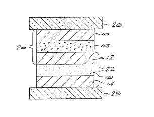
A composite radiation detection and indicating device
comprises first, third and fifth layers of a transparent
conductive material, a second layer of semiconductive
diamond between the first and third layers, and a fourth
layer of liquid crystal material between the third and
fifth layers. The layers are sandwiched together so that
a diodic structure having a radiation-dependent charge
storage characteristic is defined by the first, second
and third layers, and a liquid crystal display element
is defined by the third, fourth and fifth layers. The
invention extends to a radiation detector including the
composite device, together with an oscillator for
applying a charge to the diodic structure, and a sensor
for monitoring the decay of the stored charge. A voltage
is applied to the liquid crystal display element to cause
it to change state when the charge stored by the diodic
structure decays below a predetermined limit.
Cette invention concerne un composite détecteur-indicateur de rayonnement formé d'une première, d'une troisième et d'un cinquième couches de matériau conducteur transparent, d'une seconde couche de diamants semiconducteurs entre la première et la troisième couches et d'une quatrième couche de cristaux liquides interposée entre la troisième et la cinquième couches. Les couches sont pressées ensemble pour former une structure diode à caractéristique d'accumulation de charge fonction du rayonnement détecté, définie par les première, deuxième et troisième couches, et un élément de visualisation à cristaux liquides défini par les troisième, quatrième et cinquième couches. Cette invention concerne également un détecteur de rayonnement intégrant le composite susmentionné ainsi qu'un oscillateur servant à appliquer une charge à la structure diode et un capteur servant mesurer la décroissance de la charge accumulée. Une tension appliquée à l'élément de visualisation à cristaux liquides y engendre un changement d'état lorsque la charge accumulée dans la structure diode chute sous une valeur limite prédéterminée.
Note: Claims are shown in the official language in which they were submitted.
Note: Descriptions are shown in the official language in which they were submitted.
For a clearer understanding of the status of the application/patent presented on this page, the site Disclaimer , as well as the definitions for Patent , Administrative Status , Maintenance Fee and Payment History should be consulted.
| Title | Date |
|---|---|
| Forecasted Issue Date | 1999-03-09 |
| (22) Filed | 1990-02-02 |
| (41) Open to Public Inspection | 1990-08-03 |
| Examination Requested | 1993-08-11 |
| (45) Issued | 1999-03-09 |
| Deemed Expired | 2001-02-02 |
There is no abandonment history.
| Fee Type | Anniversary Year | Due Date | Amount Paid | Paid Date |
|---|---|---|---|---|
| Application Fee | $0.00 | 1990-02-02 | ||
| Registration of a document - section 124 | $0.00 | 1990-12-12 | ||
| Maintenance Fee - Application - New Act | 2 | 1992-02-03 | $100.00 | 1991-11-19 |
| Maintenance Fee - Application - New Act | 3 | 1993-02-02 | $100.00 | 1992-11-16 |
| Maintenance Fee - Application - New Act | 4 | 1994-02-02 | $100.00 | 1993-12-01 |
| Maintenance Fee - Application - New Act | 5 | 1995-02-02 | $150.00 | 1994-11-30 |
| Maintenance Fee - Application - New Act | 6 | 1996-02-02 | $150.00 | 1995-11-29 |
| Maintenance Fee - Application - New Act | 7 | 1997-02-03 | $150.00 | 1996-12-23 |
| Maintenance Fee - Application - New Act | 8 | 1998-02-02 | $150.00 | 1997-11-19 |
| Final Fee | $300.00 | 1998-11-19 | ||
| Maintenance Fee - Application - New Act | 9 | 1999-02-02 | $150.00 | 1998-11-20 |
Note: Records showing the ownership history in alphabetical order.
| Current Owners on Record |
|---|
| DE BEERS INDUSTRIAL DIAMOND DIVISION (PROPRIETARY) LIMITED |
| Past Owners on Record |
|---|
| JONES, BARBARA LYNN |

