Note: Descriptions are shown in the official language in which they were submitted.
y
t
7536
COLOR BALANCED IMAGE DETECTOR SYSTEM
BACKGROUND OF THE INVENTION
This invention relates to the detection of
light from a subject to obtain data suitable for the
formation of an image of the subject and, more
particularly, to the scanning of light past groups of
photodetectors arranged in rows transverse to a path of
the scanning, and wherein each group of photodetectors
is responsive to a separate portion of a spectrum of
the light.
The term "light" as used herein includes the
visible spectrum as well as invisible spectra such as
ultraviolet light and infrared light. The
photodetectors employed in the selection of the light
are fabricated generally of semiconductor materials
responsive to radiation of a specific part of the
electromagnetic spectrum such as infrared detectors or
detectors of visible light. It is common practice
today to construct an array of photodetectors upon a
common substrate of semiconductor material.
An array of photodetectors is particularly
useful in the scanning of light emitted by or reflected
from a subject to obtain data of the subject which can
be used in the construction of an image of the subject.
By scanning the light of the subject past a set of .
photodetectors, each of the photodetectors provides a
I
signal in response to the incident light. Preferably,
'the scanning is accomplished along a path perpendicular
to a line array of the photodetectors. For each scan
line, the amplitudes of the signals as a function of
time represents one line of pixels (picture elements)
in an image of the subject.
Typically, the output signal of each
photodetector is connected to electronic circuitry
which samples the output signal at a rate synchronized
with a rate of the light scanning so as to provide a
predetermined number of signal samples for each line
scanned. Signal processing circuitry extracts the
various signal samples from the photodetectors, and
arranges the samples to form an image of the subject.
Various forms of filtering may be employed on each
signal sample, or on a succession of the samples to
reduce the influence of noise so as to enhance the
image.
A problem arises in that detector elements have
a responsivity to light which varies with the frequency
of the light. The effects of the varying responsivity
are compounded by the fact that, in the case of
illumination of the subject by an external source of
light, the source of light may have an intensity which
also varies as a function of frequency. As a result,
these systems are limited in their capacity to produce
accurately a multicolored image of the subject.
For example, one method of producing a
multicolored image is to employ red, green and blue
filters in front of the, array of photodetectors to
obtain images in the primary colors of red, green, and
blue. The three images are combined to produce the
desired multicolor image. However, in view of the
foregoing variation in illuminating light and in
detector responsivity as a function of light frequency,
2
6
the relative intensities of the images in the primary
colors may be in error. An attempted correction of the
situation to produce uniformity by attenuating the
signal of the color image having an excessive intensity
simply worsens the signal-to-noise ratio with a
resultant degradation of the multicolor image.
SUMMARY OF THE INVENTION
The foregoing problems are overcome and other
advantages are provided by an imaging system employing
plural sets of detectors to provide color balanced
detection and imaging of a scanned subject. In a
preferred embodiment of the;invention, the subject,
such as a color photograph, is physically moved across
the field of view of the detectors to provide a
25 scanning of the subject line by line. Other forms of
scanning may be employed if desired. The detectors in
each set of detectors are sensitized to a specific
portion of the spectrum. In the case of a viewing of a
color subject in the visible portion of the spectrum,
red, green, and blue filters may be employed with
respective ones of the detector sets to sensitize the
respective detectors to the primary colors which will
be employed in the construction of a color image of the
subject.
In accordance with a feature of the invention,
plural sets of detectors provide compensation for
spectral variations in illumination of the subject, in
attenuation of the filters, and in sensitivity of the
photodetectors for accurate rendition of color in the
image. This is accomplished by arranging the
detectors, in each of the detector sets, in an array of
rows and columns. The columns are parallel to the _
scanning path, end the rows are transverse to the
scanning path. The detectors are constructed of
photosensitive CCD~s (charge coupled devices) which
3
operate by producing a quantity of electric charge in
response to a reception of incident light. The amount
of charge produced in a cell of the CCD array is
dependent on.the intensity of the incident~light, and
increases with increasing intensity.
A useful feature of the two-dimensional CCD
array, wherein individual cells of the array are
arranged in rows and columns, is the fact that charge
can be transferred from cell to cell along a row of the
20 array as well as from cell to cell along a column of
the array. Suitable gating circuits are available for
accomplishing the transfer of quantities of charge from
cell to cell. Also, an electrode structure is included
with each cell to activate the cell for responding to
light only during a specific sampling interval of time.
The foregoing feature of a CCD array is used
to advantage in the construction of the invention by
limiting the amount of charge produced at each sampling
of incident light to an amount of charge which is well
below the maximum amount of charge which can be held in
a CCD cell. For example, in a set of detectors having
twelve active rows of CCD cells, the scanning optics is
arranged to transmit the incident Light to induce an
increment in charge of a CCD cell which is no greater
than one-twelfth of the total charge capacity of a
cell. In the case of a detector set having sixteen
active rows of detector elements, the foregoing charge
limitation is limited to one-sixteenth of the maximum
charge which can be stored in a CCD cell.
Scanning of the subject past the detector
arrays is synchronized with~the sampling so that the
first detector element, or CCD cell, in each row
receives data from the same pixel of the subject. As
the pixel advances from row to row, the charge produced
in the cell of a previous row is transferred by the
4
gating circuitry to the cell of the next row. This
results in a summation of the charges produced by
successive samplings of the aforementioned pixel as the
pixel is scanned past successive rows of detectors in a
detector set. The resultant charge accumulated at the
last row of detectors has a much higher signal-to-noise
ratio (sNR) than would be the case for detection of a
pixel by a single detector. In the case of a detector
system employing three sets of detectors, respectively,
for the red, the green, and the blue primary colors,
the foregoing summation of charge occurs in each column
of the detector arrays in each of the detector sets.
The invention attains uniformity on color
responsivity by employing a different number of active
detector rows in each of the detector sets. It is
noted that, as a convenience in manufacture, each of
the detector sets may be constructed of the same number
of detector rows, for example, sixteen rows. Only a
relatively small number of these rows are to be
activated to detect light from that portion of the
spectrum having a relatively strong intensity of light
while, in the case of a portion of the spectrum having
a relatively weak light, a relatively large number of
the rows are activated. Typically, the red portion of
the spectrum produces the strongest illumination and
the blue portion of the spectrum produces the weakest
illumination. Accordingly, the smallest number of
active detector rows is in the red set of detectors and
the largest number of activated rows is in the blue set
of detectors.
In each of the foregoing sets of detectors, in
addition to the rows of CCD's which may serve as
detectors of light, .there is an additional row of CCD's
which receive the sum charge from each of the column of
CCD cells, this last row of CCD cells being employed as
5
CA 02009286 1999-08-27
-,
an analog shift register for transferring the sum charges from
cell to cell along the row, thereby to extract output signals of
the detection process from the array. A set of output signals
is extracted for each scan line in each CCD array. The red,
green and blue signals may be processed as by filtering and
scaling, if desired, for enhancement of the resultant image.
These signals are then employed, in accordance with well-known
image processing technology, to construct a multicolor image of
the subject.
The invention may be summarized as a color balanced
detector system comprising: plural sets of detectors, each of
said detectors detecting light from a subject, the detectors of
each of said detector sets detecting a spectral portion of the
light different from the spectral portion of the light detected
by the detectors of another of said detector sets; means for
scanning light from successive portions of the subject to said
detector sets along a predetermined scanning path; and wherein
each of said detector sets comprises a plurality of detectors
arranged in an array of rows and columns, the columns being
parallel to said scanning path and the rows being transverse to
said scanning path, each of said detectors providing a signal in
response to a detection of light; means synchronized with said
scanning means for triggering said detectors to provide their
respective signals in synchronism with the scanning along said
scanning path; means for summing signals provided by said
detectors in each column to provide a column signal for each
column of a detector set; and means for retrieving column
signals of the respective detector sets to provide imaging data
of said subject.
6
CA 02009286 1999-08-27
BRIEF DESCRIPTION OF THE DRAWING
The aforementioned aspects and other features of the
invention are explained in the following description, taken in
connection with the accompanying drawing wherein:
Fig. 1 is a stylized diagrammatic view of an imaging
system incorporating the invention, the view showing alternative
modes of scanning a subject to be viewed by plural arrays of
detectors;
Fig. 2 shows diagrammatically an array of charge-
coupled devices employed as detectors with interconnection of
the devices by gating circuitry;
Fig. 3 shows three sets of detectors employed
respectively in three detector assemblies of Fig. 1, Fig. 3
showing diagrammatically the activation of different numbers of
rows of detectors in each of the assemblies, the assemblies
being responsive to different colors of the spectrum;
Fig. 4 demonstrates graphically the accumulation of
charge in columns of the detectors of Fig. 3, each of the
detectors being charge-coupled devices connected for summing
charges of six cells, twelve cells and sixteen cells,
respectively, of the red, the green, and the blue arrays of Fig.
3;
6a
Fig. 5 is a diagrammatic view of an imaging
system of Fig. 1, constructed in accordance with a
preferred embodiment of the invention, wherein a
subject is transported by a drum past a viewing port of
the CCD detector assemblies
Fig. 6 is a block diagram of electronic
circuitry employed in the imaging system of Fig. 5;
Fig. 7 shows a case enclosing the system of
Fig. 5t
Fig. 8 is a graph shawing spectral responsivity
of a charge-coupled device to light;
Fig. 9 shows spectral output power of a lamp
which may be employed in the imaging system: and
Fig. 10 shows spectral responses of filters
which may be employed in construction of the detector
assemblies. ..
DETAILED DESCRIPTION
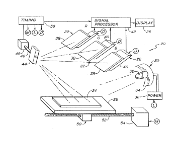
Fig. 1 shows an imaging system 20 employing
plural detector assemblies 22 positioned for viewing a
subject 24 to produce an image of the subject 24 on a
display 26. The subject 24, which may be a multicolor
photograph or other picture, by way :of example, is
supported on a table 28 and is illuminated by light of
a lamp 30. By way of example, the lamp 30 may comprise
an incandescent bulb 32 positioned in front of a
concave reflector 34 for directing rays of light
towards the subject 24.. The bulb 32 is energized with
electric current from a power supply 36.
Each of the detector assemblies 22 includes a
filter 38 and a circuit module 40 mounted behind the
filter 38. The characteristics of the filter 38 differ
for each of the detector assemblies 22, there being a
red (R) filter 38 for a first of the assemblies 22, a
green (G) filter 38 for a second of 'the assemblies 22,
and a blue (B) filter 38 for a third of the assemblies
7
38. In practice, the circuit modules 40 would have the
same physical size. However, in order to emphasize the
inventive feature wherein different numbers of rOwS Of
detectors are activated for each of the colors in order
to compensate for differences in spectral responsivity,
the module 40 shown behind the red filter is shown
having a narrow configuration, the module 40 behind the
green filter is shown having a medium-size width, and
the module 40 behind the blue filter is portrayed with
a maximum width. The circuit modules 40 output signals
in response to the reception of incident light, the
signals outputted by the modules 40 being applied to a
signal processor 42 for generation of the image to be
presented on the display 26.
25 Tn order to demonstrate the scanning aspect of
the imaging system 20, two possible modes of scanning
are shown in Fig. 1, namely, a mirror 44 and associated
optics (not shown) which is rotated about a shaft 46 of
a motor 48, and a lead screw drive 50 which translates
the table 28 in response to rotation of a lead screw 52
by a motor 54. Rotation, or pivoting, of the mirror 44
and translation of the table 28 are synchronized with
operation of the detector assemblies 22 and the signal
processor 42 by a timing unit 56 which provides timing
signals for driving the motors 48 and 54 and for
operating the circuit modules 40 and the processor 42.
If desired, a timing signal, outputted by the unit 56
at terminal L may be employed for activating the power
supply 36 for lighting the lamp 30 a predetermined
amount of time prior to operation of either of the
scanning devices to insure that the temperature of the
bulb 32 has stabilized for a uniform spectral output to
the light. Signals from the timing unit 5s to the
motor 54 and to the detector assemblies 22 are
indicated, respectively, by terminals labeled M and D.
8
It is to be understood that, in practice, only
one of the scanning devices of Fig. 2 would be employed
in the operation of the system 20. For example, if
scanning is to be'done by operation of the mirror 44,
then the lead screw drive 50 and the table 28 would
remain stationary. Alternatively, if scanning is to be
done by translation of the table 28, then the mirror 44
would remain stationary while the lead screw 52 would
rotate to translate the table 28 and the subject 24.
Yet a third configuration of the scanning device, with
use of a rotating drum, is to be employed in the
preferred embodiment of the invention as will be
described subsequently with reference to Fig. 5.
Fig. 2 shows details in the'~construction of a
circuit module 40 of Fig. 1. Each of the modules 40 is
constructed in the same fashion. The module 40 '
comprises a plurality of CCD registers 58 positioned
transversely to a direction of a scanning of a light
beam incident upon a detector assembly 22 (Fig. 1) in
response to a scanning of the subject by either the
mirror 44 or the~drive 50 (Fig. 1). The direction of
scanning is indicated by an arrow 60. In Fig. 2, the
subject 24 is shown as having an arbitrary shape, and
further includes two rows of four pixels each. The
pixels are presented as little circles identified by
the legends A1-A4 in the first,row, and B1-B4 in the
second row. Tn the preferred embodiment of the
invention, 16 of the registers 58 are employed in the
CCD array of detectors, with each register having 2048
cells capable of detection of light. A further
register is employed for extracting signal samples
obtained from the detection of light by cells of the
CCD array. The signal samples are obtained from a
plurality of the other sixteen registers.
9
a ~~~~~~i
By way of example, and to simply the
description, the portrayal of the circuit module 40 in
Fig. 2 shows a total of only four registers 58 each of
which has only four cells. In the uppermost register
58, the cells are identified by the legends J2-J4: in
the next register 58, the cells are identified by 'the
legends K1-K4; and in the following register the cells
are identified by the legends L1-L4. These three
registers are employed for the detection of light. The
last of the registers 58, at the bottom of the array of
Fig. 2, has cells identified by the legends M1-M4, and
is employed fo.r extracting signal samples from the
module 40. Also included within the circuit module 40
is a set of gates 62, 64, 66, and 68 which are driven
by a gate driver 70. An amplifier 72 is connected to
an output terminal of the fourth register 58 fox
applying signals outputted by the fourth register 58 to
the signal processor 42.
Tn operation, the gate 62 applies a signal via
line 74 to activate an electrode assembly (not shown)
in each of the cells J1-J4 to render these cells
responsive to incident light for detecting the light
during a sampling interval of time designated by an
electrical pulse signal on line 74. Similarly, the
gate 64 applies a sample pulse.signal via a line 76 to
activate the corresponding electrode structures (not
shown) of the cells K1-K4, and the gate 66 similarly
applies, via line 78, an electric pulse signal to the
electrode structures of the cells L1-L4 to initiate
sampling of incident light by the cells. Circuitry of
the gate 62 also extends between the first two
registers 58 for transferring charge between a first
cell in each column to a second cell in each column.
Thus, upon activation of circuitry within the gate 62,
charge in the cell J1 is transferred into the cell K1,
la
~~~:~r~~~
charge in the cell J2 is transferred to the cell K2,
with similar charge transfers being accomplished
between the cells J3-K3 and J4-IC4. In a similar
fashion, circuitry of the gate 64 and of the gate 66
~5 provides for further transfer of charge among the cells
of the individual columns, namely, successive transfers
of charge among the cells K1-L1-M1 through K4-L4-M4.
Circuits of the gates 62, 64, 66, and 68 are activated
by the driver 70 in response to signals of the timing
unit 56. The array of the charge-coupled devices of
the four registers 58 in conjunction with the circuits
of the gates 62, 64, 66, and 68 operate in accordance
with a gating procedure known as a three-phase gating
operation.
With reference also to Figs. 3 and 4, there are
shown further aspects in the summation of signals in
the various columns of the array of Fig. 2. Fig. 3
shows three detector arrays of the three detector
assemblies 22 of Fig. 1, namely, the red assembly, the
green assembly, and the blue assembly. In the red
array, shown at the top of Fig. 3, there axe only six
of the registers 58 exposed to incident light,.the
remaining ten registers being covered from the light so
as to render them nonresponsive to the incident light.
In the green array, shown in the middle of Fig. 3,
there are twelve rows of registers 58 exposed for
detection of incident light. In the blue array at the
bottom of Fig. 3, there are sixteen rows of registers
58 exposed for the selection of incident light. The
bottom register of Fig. 2 containing the cells M1-M4 is
represented in each of the three arrays of Fig. 3 as a
solid line at the bottom of the array to simplify the
drawing in Fig. 3.
The aspect of summation for integration of the
signals obtained from each pixel of the subject for
11
~~~~~~i
forming the corresponding pixel of the image may be
explained with reference to Figs. 2, 3, and 4.
Consider the pixel A1 (Fig. 2) in the subject 2~.
During an early part of the scan, the pixel A1 reflects
light of the lamp 30 to be detected by the cell J1 of
the charge-coupled device of the register 58. The cell
J1 produces an electric charge proportional to the
reflectivity of light from the pixel A1. The resulting
charge produced in the cell J2 is transferred by the,
gate 62 to the cell K1. Subsequently, as the scanning
motion of the rays of light continue, rays of light
from the pixel A1 impinge upon the cell K1. At this
point in time, the driver 70 activates circuitry of the
gate 64 to energize the electrode structure of all of
the cells of the second register 58, thus enabling the
cell K1 to sample the light from the pixel A1.
Upon a sampling of the light of pixel A1 by
cell K1, additional charge is produced by the cell K1.
The~total charge now present in the cell K1 is equal to
the sum of the charges produced by the detection
operations of cells J1 and ~cl. Thereafter, the gate 64
transfers the~charge from K1 to the cell L1, this being
followed by a further sampling of light of the pixel A1
with the further production of charge to produce a
total charge accumulation in the cell.Ll equal to the
sum of the charges produced by the detection of light
from the pixel A1 by the cells J1, K1, and L1.
At the time when the cell K1 is being activated
to sample light of the pixel A1, the cell J1 is being
activated to sample light of the pixel B1. Therefore,
the sum of charges appearing in cell L1 at the
conclusion of three sampling intervals of the pixel A1
is succeeded in next sampling interval with a sum of
the charges from the sampling of the pixel 81. Similar
comments apply to the summation of pixel signals via
12 _
the columns J2-K2-L2, J3-K3-L3, and J4-K4-L4. At the
conclusion of the sampling of the respective rows of
pixels by the third register 58, the resultant
accumulated charges are transferred by the gate 66 to
the corresponding cells M1-M4 of the fourth register
58. Thereupon, -the gate 68 is activated by the driver
7o in response to timing signals from the timing unit
56 to strobe the cells M1-M4 to shift the charges
through the fourth register 58 and via the amplifier 72
to the signal processor 42. Thus, the accumulated
charge in cell M4 is transferred out by the amplifier
72, the accumulated charge in the cell M3 is
transferred into the cell M4., the accumulated charge in
the cell M2 is transferred into the cell M3, and the
I5 accumulated charge of the cell M1 is transferred into
the cell M2. Subsequent transfers allow the various
quantities of charge to move sequentially through the
cells of the fourth register 58 to~be stored in the
processor 42 for subsequent use in forming the image.
The charges of the fourth register 58 are cleared out
completely prier to the next sampling interval, so as
to be ready to receive charges from the next row of
pixels.
The summation of the relatively high intensity
red signals is accomplished within six scanning
intervals by use of the six registers 58 shown at the
top of Fig. 3. The summation, or integration, of the
six signal samples is represented graphically in the
left hand trace of the graph of Fig. 4. The signal
samples, herein, are understood to be the charges
produced in the CCD cells in response to the viewing of
a sample of the incident light. The weaker green
signals outputted by cells of the green array are
attained through twelve steps of summation, indicated
in the middle trace of Fig. 4, and are produced by use
13
of the twelve registers 58 of the green array.
Similarly, the weakest blue signals are accumulated via
sixteen steps, shown in the right hand trace of Fig. 4,
and are produced by summation of the samples attained
by the sixteen rows of the blue array at the bottom of
Fig. 3.
As noted in Fig. 1 and Fig. 3, the detector
arrays of the three assemblies 22 are arranged side-by-
side. Therefore, the pixel A1 (Fig. 2) is first
20 detected by elements of the red assembly 22, and
thereafter by elements of the green assembly 22, and
finally by the elements of the blue assembly 22. Thus,
the signal processor 42 receives red image data, green
image data, and blue image data. The image data of the
various pixels of the three different colored images
are placed in registration by the processor 42, in
accordance with well-known image processing operations,
to provide an output colored image on the display 26,
as by illuminating red, green and blue phosphors of a
television type of screen (not shown) in the display
26.
With reference to Fig. 5, there is shown an
imaging system 20A which is a preferred embodiment of
the system 20 portrayed in Fig. 1. The principles of
the invention set forth in the description of the
system of Fig. 1 apply also to the embodiment of Fig.
5. The system 20A of Fig. 5 comprises a bed 80 upon
which the subject 24 is advanced for viewing by a CCD
detector assembly 82. At an aperture 84 in the bed 80,
there are located interfacing surfaces of a drum 86 and
two rollers 88 and 90 which press against the drum 86
in the absence of the subject 24, and which squeeze the
subject 24 against the drum 86 during presence of the
subject 24 at the aperture 84. The drum 86 is driven
by a stepper motor 92 connected to the drum 86 by a
14
belt 94 driven by an output pinion 96 of the motor 92.
The surface of the drum 86 provides a secure friction
grip with the subject 24.so as to advance the subject .
24 in a line-by-line fashion in response to successive
rotational increments of the motor 92. Tnterrupters 98
and 100 are provided for signaling locations of edges
of the subject 24. Each of the interrupters 98 and 100
may be constructed in a well-known fashion employing an
LED (light-emitting diode) transmitter and receiver for
generating an electric signal designating the presence
or absence of an LED beam of light due to the absence
of or presence, respectively, of the subject 24.
Light illuminating the subject 24 is provided
by the lamp 30, previously described in Fig. 1. Rays
of light from the lamp 30 are reflected off of a planar
mirror 102 and pass through a polarizer 104 onto the
site where the subject 24 is to be viewed. The viewing
site is located midway between the two rollers 88 and
90 on the front surface of the subject 24, as the
subject 24 presses against the surface of the drum 86.
It is noted that the subject 26 is placed initially on
the bed 80 manually, and guided manually through the
first interrupter 98 up to the roller 88, at which
point the roller 88 with the drum 86 grab the leading
edge of the subject 24 to automatically feed the
subject 24 through the viewing site. Rays of light
reflected from the subject 24 propagate along an
optical path undergoing reflection sequentially at two
mirrors 106 and 108 and pass through a second polarizer
210 and a focusing lens 112 to impinge upon the CCD
detector assembly 82.
The two polarizers 104 and 110 are useful in
enhancing the SNR by excluding unwanted scattered light
from scratches that may be on the subject 24> The
concavity of the reflector 34 of the lamp 30 provides
for a uniform illumination of the successive scan lines
of the subject 24, and the lens 112 brings the scan
lines successively to a sharp focus upon the array of
CCD cells in the CCD detector assembly 82. Output
signals of the CCD detector assembly 82, produced upon
detection of the pixels of the successive scan lines of
the subject 24, are applied to a suitable signal
processor (not shown in Fig. 5) for developing of an
image as has been described in Fig. 1.
Fig. 6 shows electrical circuitry connected to
elements of the system 20A shown in Fig, 5. Fig. 6
shows the CCD color detector assembly 82, the lamp 30,
the interrupters 98 and 100, and the stepper motor 92
disclosed in Fig. 5. rn Fig. 6, red, green and blue
output signals of the detector assembly 82 are
multiplexed by a multiplexes 114 and applied to an
analog-to-digital converter 116. The converter 116
provides for nine-bit digital signals. The circuitry of
Fig..6 further comprises a digital signal processing
unit 118, a look-up table (read-only memory) 120, an
optional color enhancement and sharpening unit 122, a
sCSI (small computer system interface) 124, a
microcontroller or computer 126, a timing unit 128 for
operation of CCD circuits in the assembly 82, and LED
(light-emitting diode) 130 and a calibration button
132. The signal processing unit 118 provides for
brightness correction, uniformity correction, and
resolution control. This is accomplished by use of the
nine-bit digital words from the converter 116.
Resolution control can be attained in one
dimension by advancing the subject 24 a greater
distance between successive line scans and by advancing
the charge at a higher rate proportional to the
increase in scanning speed. Resolution in a direction
transverse to the direction of movement of the subject
16
~
~~~:~r~~l~i
24 can be reduced by skipping over adjacent cells of
the CCD registers 58 (Fig. 2). By averaging pairs of
the cells, the resolution is cut in half. This permits
the resolution to be selected in accordance with needs
of a user of the imaging system. Output signals of the
processing unit 218 are converted to 8-bit bytes at the
look-up table 120, and then applied to the enhancement
circuit 122 to be outputted via the SCSI interface 124,
the interface 124 being suitable for outputting data to
certain computers (not shown) employing such interface
for display of an image on a screen of the computer.
Control of motion of the subject 24 is
accomplished in accordance with the following
procedure. The first interrupter 98, upon sensing the
leading edge of the subject 24, signals the controller
126 to activate the stepper motor 92 in the forward
direction for advancing the subject 24 along the bed
80. With reference also to Fig. 7, the forward driving
of the motor 92 draws the subject 24 into an entrance
port 134 of a case 136 which encloses the system 20A.
The subject 24 continues to pass along the bed 80 on a
path through the second interrupter 100, the drum 86
continuing to advance the subject 24 until the leading
edge thereof has passed through both of the
interrupters 98 and 100.
A predetermined time after the interrupter 98
shows the absence of the subject 24, the controller 126
responds by reversing the direction of the motor 92,
and by operating the motor 92 in a relatively low
speed, Line-by line scanning mode. The controller 126
activates the timing unit 128 to operate the CCD
registers of the assembly 82, and to conduct the
imaging operations in the manner taught with respect to
Fig. 1. In the system 2OA, the imaging operations
include signal processing by the processingwnit 118
17
~~~~~~F'
and the enhancement unit 122. Operation of the units
118 and 122 is directed by the controller 126. As the
subject 24 proceeds in the reverse direction along the
bed 80, the subject 24 passes through the interrupters
100 and 98. Upon clearing the interrupter 100, the
stepper motor 92 is stopped within a predetermined time
interval by the controller 126, at which point in time
the subject 24 extends from the port 134 of the case
136.
The LED 130 is located on the front side of the
case 136. The calibration button 132 is mounted
alongside the LED 130. The controller 126 operates the
LED 130 to light the LED when the system is ready to
receive the subject, the LED 130 being off during
scanning of the subject 24. The controller 126 causes
the LED 130 to blink at the conclusion of a scanning
process. The calibration button 132 signals the
controller 126 to operate the scanning process with a
test subject. If desired, the lamp 30 may include a
halogen gas activated~by a tungsten filament, and may
include an infrared filter to prevent excessive heating
of the subject 24.
Figs. 8, 9, and 10 show variations in response
as a function of wavelength of the light. Fig. 8 shows
the variation in responsivity of a CCD fabricated of
silicon as a function of wavelength, the responsivity
being based on the number of amperes of CCD current
generated per watt of detected radiation. The
responsivity peaks at a region between blue and green
light. Fig. 9 shows variation in the relative power
outputted by the lamp employed for illuminating the
subject. 'fhe radiation emitted by the lamp has a peak
power at approximately 700 nm (nanometers) wavelength
and drops to zero at approximately 360 nm wavelength.
This corresponds to a relatively high intensity in the _.,
18
red portion of the spectrum and relatively low
intensity at the blue portion of the spectrum. Fig. 10
shows the transmission characteristic of a bandpass
filter employed for blue light, a bandpass filter
employed for green light, and a pair of two filters,
namely a law pass filter and a high pass filter, which
are combined to provide a single passband for red
light. on the vertical axis, 100 percent represents
complete transparency, with the lower values indicating
attenuation at optical signals propagating through the
filters.
A combination of the responsivities of the
foregoing three graphs are employed to determine the
amount of compensation required by the three sets of
CCD registers disclosed in Fig. 3, wherein a larger
number of registers are required to detect light when
the light is of a low intensity, and wherein a smaller
number of registers are activated to detect light when
the light is of a relatively high intensity. The
foregoing teaching of the invention provide a more
uniform production of images with respect to the
various color components while maintaining a high
signal-to-noise ratio for accurate production of an
image of the subject.
It is to be understood that the above described
embodiment of the invention is illustrative only, and
that modifications thereof may occur to those skilled
in the art. Accordingly, this invention is not to be
regarded as limited to the embodiment disclosed herein,
but is to be limited only as defined by the appended
claims.
19