Note: Descriptions are shown in the official language in which they were submitted.
FJ-7636
- 1 2009315
AMPLIFYING CIRCUIT
BACKGROUND OF THE INVENTION
l. Field of the Invention
The present invention relates to an amplifying
circuit including a bias circuit, and more particularly,
to bias circuits for making the characteristics of a
plurality of amplifying transistors coincide.
In the case of a balanced amplifier in which
an input is divided into two branches which are
respectively amplified by amplifying transistors such as
field effect transistors (herein after referred to as
FETs), and the outputs thereof are combined to obtain a
desired output, or in the case of supervising an input
level of a mixer by dividing the output of the balanced
amplifier into two branches, one of which is input into
the mixer for effecting a frequency conversion and the
other of which is measured, it is necessary to coincide
the output power of the two FETs. The adjustment for
this is effected by setting the drain voltages VDs and
the drain currents ID of the FETs.
To achieve this effect, a bias circuit is
desired in which the drain currents ID can be kept
constant and the drain voltages VDs can be changed
independently from the drain currents ID I and the
number of adjusting points is kept as small as possible.
2. Description of the Related Arts
In a conventional balanced amplifier, the
drain current and the drain voltage of each FET are
respectively adjusted by variable resistors, however,
there are problems in that a large number of expensive
variable resistors are necessary and the adjustment of
the drain currents is troublesome, as later described in
more detail with reference to the drawings.
In another conventional balanced amplifier,
the drain current and the drain voltage of each FET are
automatically determined by employing a bias transistor.
~ - 2 - 2009315
In this case, however, the drain voltage cannot be
determined independéntly from the determination of the
drain current, as later described in more detail with
reference to the drawings.
SUMMARY OF THE INVENTION
Accordingly, an object of the present invention is
to provide an amplifying circuit with a bias circuit
which can determine the drain voltage independently from
the determination of the drain current while the drain
current is kept constant, with a small number of
adjusting points and at a low cost.
To attain the above object, there is provided,
according to the present invention, an amplifying
circuit comprising at least one amplifying transistor
for amplifying an input signal, and at least one bias
circuit for determining a current passing through the
amplifying transistor and for determining an output
voltage at the output of the amplifying transistor. The
bias circuit comprises a current determining circuit
including a current determ;ning transistor, connected to
the amplifying transistor, for determining a current
passing through the amplifying transistor, and a voltage
determining circuit including a voltage determining
transistor, connected to the amplifying transistor, for
determining an output voltage at the output of the
amplifying transistor, the output voltage being
determined independently from the determination of the
current.
By the current determining transistor, the current
passing through the amplifying transistor is determined.
By the voltage determining transistor, the output
voltage of the amplifying transistor is determined
independently from the current passing through the
amplifying transistor.
3 5 BRIEF DESCRIPTION OF THE DRAWINGS
The above object and the features of the present
invention will be more apparent from the following
_ 3 _ 20093~
description of the preferred embodiments with reference
to the drawings, whérein: -
Figure lA is a circuit diagram showing anexample of a conventional amplifier circuit including
two amplifying FETs and two bias circuits;
Figure lB is a block diagram showing a mixer
and a monitor to which the outputs of the amplifier
circuit shown in Fig. lA are applied;
Figure lC is a block diagram showing a hybrid
circuit for combining the outputs of the amplifier
circuit when the amplifier is used as a balanced
amplifier;
Figure 2 is a circuit diagram showing another
example of a conventional amplifier circuit including a
bias circuit;
Figure 3 is a circuit diagram showing an
example of an amplifier circuit employing variable
resistors in the bias circuits, considered before
conceiving the present invention;
Figure 4 is a circuit diagram showing an
amplifier circuit including a bias circuit according to
an embodiment of~the present invention;
Figures 5A and 5B are circuit diagrams showing
an amplifier circuit according to an embodiment of the
present invention; and
Figure 5C is a block diagram of a mixer and a
monitoring circuit to which the outputs of the amplifier
circuit are applied according to the embodiment of the
present invention.
DESCRIPTION OF THE PREFERRED EMBODIMENTS
For better understanding of the present invention,
conventional amplifier circuits and the problems therein
will first be described with reference to Figs. lA, lB,
lC and 2.
Figure lA is an example of the construction of a
balanced amplifier. In the figure, a high frequency
input signal applied to an input terminal IN is divided
2009315
-- 4
by a hybrid circuit (Hl) 11 into two branches which are
amplified by two amplifying transistors (FETl and FET2)
12 and 13. As an application of the balanced amplifier,
one of the outputs at the output terminals OUT1 and OUT2
may be applied as an input signal of a mixer (RF/IF) 102
in a heterodyne receiver having a radio frequency
amplifier (RFA) 101, the mixer (RF/IF) 102 for
converting the radio frequency into an intermediate
frequency, an intermediate frequency amplifier
(IFA) 103, and the other output at the output
terminal OUT2 being monitored by a monitoring unit 104,
as shown in Fig. lB. As an another application of the
balanced amplifier, the output signals at the output
terminals OUT1 and OUT2 are combined by a hybrid circuit
(H2) 105, as shown in Fig. lC, to obtain a desired
output signal.
Referring back to Fig. lA, a resistor 14 having
a resistance R1 and a variable resistor 15 having a
variable resistance VRl are connected in series between
a power supply voltage VGG and ground. The gate voltage
of the transistor 12 is determined by the resistors 14
and 15. Therefore, the gate voltage of the
transistor 12 can be adjusted by adjusting the variable
resistor 15. The drain current passing through the
transistor 12 is determined by its gate voltage.
Once the drain current ID is determined, the drain
voltage VDs at the output terminal OUTl is determined by
adjusting a variable resistor (VR3) 18 connected between
the power supply voltage VDD and the drain of the
transistor 12. In this case, in bias setting circuits
consisting of a resistor R1 and a variable
resistor VRl , and a resistor R2 and a variable
resistor VR2 , the drain currents ID are respectively
set to predetermined values by adjusting the gate
voltages vGs by means of VRl and VR2 , and the drain
voltages VDs are respectively set by adjusting the
variable resistors VR3 and VR4 provided in the drain
_ 5 _ ~ n~ 9
circuits.
Similarly, the drain current passing through the
other transistor 13 can be determined by adjusting a
variable resistor (VR2) 17, and the drain voltage of the
transistor 13 can be determined by adjusting a variable
resistor (VR4) 19.
In the circuit shown in Fig. lA, there are various
problems as follows.
(1) When one of the outputs is input into the
local oscillator circuit and the other output is
monitored as shown in Fig. lB, or when the two outputs,
are combined to obtain a desired output, the two output
powers should be the same. In the circuit shown in
Fig. lA, the drain currents are set by adjusting the
variable resistors 15 and 17 separately, and the drain
voltages are set by adjusting the variable resistors 18
and 19 separately. In other words, the drain currents
cannot be set by adjusting a single variable resistor.
This is because the field effect transistors 12 and 13
do not always have the exact same characteristics due
to variations in their manufacturing processes.
Therefore, there are a number of adjusting points
in the circuit shown in Fig. lA. Further, it is
necessary to measure the drain currents. Accordingly,
the circuit shown in Fig. lA has a disadvantage in that
the adjustment and the measurement of the drain currents
are troublesome.
(2) The circuit shown in Fig. lA requires a number
of variable resistors. Since variable resistors are
expensive, it is not preferable to use a number of them.
(3) Even after the drain currents are set to a
desired value by adjusting the variable resistors 15 an
16, when a high voltage signal is applied at the input
terminal IN, a gate current IG flows due to a forward
bias between the gate and the N channel so that the gate
voltage VGs changes, and accordingly, the drain
current ID changes. In particular, when the output
20~93 1 S
signal of the amplifier shown in Fig. lA is applied to
the mixer 102, and output signal of a local oscillator
(not shown) is applied to the input terminal IN of the
amplifier shown in Fig. lA, and, to make the output
power level of the amplifier constant, the input level
of the amplifier, which is the output level of the local
oscillator, is often made so high that the output level
of the amplifier is saturated. In this case, when the
output level of the local oscillator fluctuates due to
temperature changes and so forth, the gate current IG
changes so that the gate voltage VGs changes, and
accordingly the drain current ID changes. As a result,
the fluctuation of the output level of the local
oscillator is undesirably amplified.
Because of this, it has been desired to obtain
a bias circuit in which the drain voltage VDS can be
changed independently from the drain current ID while
the drain current ID is kept constant.
Figure 2 is a circuit diagram showing another
example of a conventional amplifier circuit including a
bias circuit in which the gate voltage VGs is
automatically adjusted so as to make the drain
voltage VDs and the drain current ID constant. If two
outputs are necessary as in the balanced amplifier shown
in Fig. lA, two circuits each being the same as the
circuit shown in Fig. 2 may be provided.
In the circuit shown in Fig. 2, when the
positive power supply voltage VDD and the negative power
supply voltage VGG are constant, the drain voltage VDs
of the amplifying transistor (FET1) 21 is determined as:
DS B1
by applying a base voltage VB1 determined by the ratio
of resistors (R1 and R2) 23 and 24 connected in series
between the power supply voltage VDD and the negative
power supply voltage VGG. The current passing through a
resistor 26 having a resistance R4 connected between the
drain of the amplifying transistor 21 and the positive
- 200931 5
-- 7
power supply voltage VDD is shunt through the field
effect transistor (FET1) 21 and a pnp transistor (Tr1)
22, however, most of the current flows through the field
effect transistor 21. Therefore, the drain current ID
is determined by dividing the voltage between the
positive power supply voltage VDD and the drain
voltage VDs , by the resistance R4. In this case, the
gate voltage VGs is automatically adjusted by the
transistor Tr1 in such a way that the drain voltage VDs
becomes the above mentioned value. Namely, when the
drain current ID is increased, the drain voltage VDs
which is the same as the emitter voltage of the
transistor 22 is lowered, so that the collector voltage
of the transistor 22 and thus the gate voltage of the
transistor 21 is lowered, resulting in a decrease of the
drain current ID so that the drain voltage VDS is
raised.
In the circuit shown in Fig. 2, the drain
voltage VDS is set by the ratio between the resistors R
and R2 ~ and the drain current ID changes when VDS
changes. Namely, once the drain voltage VDs is
determined, the drain current ID can be set
independently from the drain voltage VDS by changing the
resistance R4.
However, if the drain voltage VDs changes, the
drain current ID also changes. In other words, in the
circuit shown in Fig. 2, the drain voltage VDS cannot be
changed while the drain current ID is kept constant.
When the output of the amplifier shown in Fig. 2 is
applied to the input of the mixer 102 shown in Fig. lB,
it is often necessary to independently change the drain
voltage VDS while the drain current ID is kept constant.
Therefore, the amplifier shown in Fig. 2 cannot be
applied as an input circuit of the mixer 102.
Figure 3 is a circuit diagram showing an
example of an amplifier circuit employing tandem type
variable resistors in the bias circuits, considered
2009315
-- 8
before conceiving the present invention, in which
amplifying transistors (FET1 and FET1a) 31 and 31a are
field effect transistors intended to have the same
characteristics, transistors (Tr1 and Tr1a) 32 and 32a
are bipolar transistors, 33 to 36 are resistors having
resistances Rl to R4 , 35a and 36a are resistors having
resistances R3a and R4a. 37 and 37a are tandem type
variable resistors having resistances R5 and R5a which
are the same.
In the circuit shown in Fig. 3, since the
tandem type variable resistors 37 and 37a are inserted
in the drain circuits of the amplifying transistors
(FETl and FET1a) 31 and 3la, the drain voltages can be
changed independently from the respective drain currents
by adjusting the resistors 37 and 37a. Namely, the base
voltage of the transistors 32 and 32a is determined by
the resistors 33 and 34 connected between the power
supply voltage VDD and the negative power supply
voltage VGG. The emitter voltage of the transistor 32
is determined by the base voltage plus the emitter-base
voltage which is constant and approximately 0.6 V.
Thus, the drain current passing through the
transistor 31 is determined by dividing the voltage
between the emitter of the transistor 32 and the power
supply voltage VDD by the resistance R4 of the
resistor 36. The drain voltage of the transistor (FET1)
31 is then determined by adjusting the variable
resistor 37. Similarly the drain voltage of the
transistor 31a is determined by adjusting the variable
resistor 37a.
Therefore, in the circuit shown in Fig. 3, the
output voltage at the output terminal OUT1 or OUT2 can
be changed independently from the drain current ID / and
the drain current ID can be changed independently from
the output voltage. However, there is a problem in that
an increase in the cost cannot be avoided because two
variable resistors of the tandem type are necessary when
2009315
applied to a balanced amplifier and so forth, and the
respective variable resistors must be adjusted so that
the drain voltages of both the FETs are coincident, thus
requiring tandem type variable resistors having the same
characteristics.
In the present invention, such problems
in the conventional arts are intended to be solved,
and the present invention has an object to provide
a bias circuit in which a drain voltage VDs can be
set independently while the drain current ID of the
FET is kept constant, and which has a small number
of adjusting points so that it can be constructed
at a low cost.
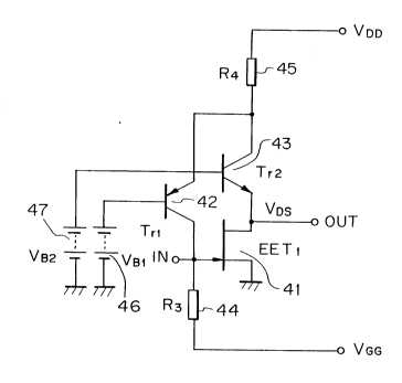
The principle construction of an embodiment of
the present invention is as shown in Fig. 4, in which an
amplifying transistor (FETl) 41 is an N channel field
effect transistor (FET) of a junction type, a pnp
transistor (Tr1) 42 is a drain current determining
transistor, and an npn transistor (Tr2) 43 is a drain
voltage determining transistor. The drain current
determining transistor 42 has a base connected to
receive a first bias voltage VBl from a first bias
voltage source 46, an emitter connected through a drain
current determining resistor 45 having a resistance R4
to a positive power supply voltage VDD , and a collector
connected to the gate electrode of the amplifying
transistor 41. The drain voltage determining
transistor 43 has a base connected to receive a second
bias voltage VB2 from a second bias voltage source 47, a
collector connected through the resistor 45 to the
power supply voltage vDD , and an emitter connected to
the drain of the amplifying transistor 41. The gate
electrode of the amplifying transistor 41 is connected
to an input terminal IN. The drain of the amplifying
transistor 41 is connected to an output terminal OUT.
The source electrode of the amplifying transistor 41 is
connected to ground. The gate electrode of the
- 10 - 209315
amplifying transistor 41 is connected through a
resistor 44 to a negative power supply voltage VGG.
The second bias voltage VB2 should be lower
than the power supply voltage VDD. The first bias
voltage VB1 plus the emitter-base voltage of the
transistor 42 should be lower than the second bias
voltage VB2.
In operation, the drain current of the
amplifying transistor 41 is set by adjusting the base
voltage of the transistor Tr1. Namely, the emitter
voltage of the transistor 42 is determined as VB1 plus
emitter-base voltage of the transistor 42, and the
current passing through the resistor 45 is determined by
dividing the voltage between VDD and the emitter voltage
of the transistor 42 by the resistance R4. The drain
voltage of the amplifying transistor 41 is set by
adjusting the base voltage of the transistor Tr2.
Namely, the drain voltage can be determined as the
voltage VB2 minus the base-emitter voltage of the
transistor 43, independent from the determination of the
drain current.
Figs. 5A is a circuit diagram of a balanced
amplifier according to an embodiment of the present
invention. In Fig. 5A, the same reference numerals as
those in Fig. 4 represent the same parts. Similar parts
as the parts 41 to 45 are respectively represented by
symbols 41a to 44a. There are two amplifying circuits,
one being formed by the parts 41 to 45 and the other
being formed by the parts 41a to 45a. A resistor 51
having a resistance Rl and a resistor 52 having a
resistance Rz are connected in series between the
positive power supply voltage VDD and the negative power
supply voltage VGG. The connecting point of the
resistors 51 and 52 is commonly connected to the bases
of the transistors 42 and 42a. By this arrangement, the
first bias voltage VBl in Fig. 4 is realized in Fig. 5A.
A variable resistor 53 having a variable resistance VR1
2009315
11
is connected between the positive power supply
voltage VDD and the negative-power supply voltage VGG.
The intermediate point of the variable resistor 53 is
commonly connected to the bases of the transistors 43
and 43a. By this arrangement, the second bias
voltage VB2 in Fig. 4 is realized in Fig. 5A.
The gate electrode of the amplifying
transistor 42 is connected to a first input
terminal IN1. The gate electrode of the amplifying
transistor 43 is connected to a second input
terminal IN2. The drain of the amplifying transistor 41
is connected to a first output terminal OUT1 , and the
drain of the amplifying transistor 41a is connected to a
second output terminal OUT2.
When the amplifying circuit shown in Fig. 5A is
used as a balanced amplifier, an input signal from an
oscillator circuit (not shown) and applied to an input
terminal IN is divided into two branches by a hybrid
circuit 58 as shown in Fig. 5B, and the two outputs
thereof are applied as the input signals to the input
terminals INl and IN2. One of the two output signals
output from the output terminal OUT1 may be applied as a
local oscillator input to a mixer 502 connected between
a radio frequency amplifier 501 and an intermediate
frequency amplifier 503, and the other output signal may
be monitored by a monitoring unit 504 as shown in
Fig. 5C.
In the circuit shown in Fig. 5A, by the
circuit including the transistors 41 and 41a, and the
resistors 44, 45, 51, and 52, the gate voltage of the
amplifying transistors 41 and 41a are automatically
adjusted so as to make their drain currents constant.
Also, the drain voltages are arbitrarily set by
adjusting the variable resistor 53.
Accordingly, by the circuit of Fig. 5A, the
respective drain voltages can be changed simultaneously
and with a good balance by adjusting the variable
- 12 - 200931 S
resistor 53 while the drain currents of the amplifying
transistors 41 and 41a are kept constant.
Any number of the amplifying field effect
transistors which should have the same characteristics
as those of the field effect transistor 41 may be
provided according to the present invention.
Note that, in the circuit of Fig. 5A, instead
of the N channel FETs, P channel FETs may alternatively
be used. Further, the polarities of the npn and pnp
bipolar transistors may be reversed with the reverse of
the polarities of the power supply voltages. Namely,
each transistor may be changed to npn type or pnp type,
and in this case the polarities of the power supplies
may also be changed.
Also, as the amplifying transistor 41 and 41a,
not only the junction type field effect transistors, but
also MOS FETs or bipolar transistors may be used. In
this case, the power supply VGG is not restricted to the
negative power supply but may be ground for example.
Also, when it is used in a balanced amplifier,
a mixer and so forth, it is a matter of course that
necessary high frequency circuits are connected to the
gate sides and the drain sides of respective FETs,
although they are omitted in Fig. 5A.
As described above, according to the present
invention, in a bias circuit in which the gate voltages
are automatically adjusted in such a way that the drain
currents of a plurality of FETs become a designated
value, since drain voltage determining transistors are
provided in series with the drain circuits of the FETs,
the drain voltages of the respective FETs can be
adjusted simultaneously with a good balance by means of
only one variable resistor while maintaining the drain
currents to be constant, so that the adjustment is easy
and the device is economical.