Note: Descriptions are shown in the official language in which they were submitted.
2~ 3432
PROGRAMMABLE DATA PACKET BIJ~
PRIORITIZATION ARRANGEMENT
Field of the Invention
The invention relates to an arrangement for storing a data word
5 in a buffer memory, and more particularly relates to an arrangement which
either stores an incoming data word in memory or discards the data word
based on the priority level of the data word.
BackRround of the Invention
In a packet switched network it is more economical to store
10 system control packets and client data packets in a common buffer, rather
than in dedicated buffers. However, it is possible that a common buffer
could overflow during periods of heavy data traffic, thereby resulting in the
loss of one or more system control packets. A loss of a system control
packet could lead to a degradation in the performance and reliability of the
15 packet switched network.
Sllmrn~ry of the Invention
The chance of possibly losing a system control packet due to a
buffer overflow condition is greatly reduced by ensuring that sufficient
space is reserved in a common buffer for the storage of system control
20 packets. Specifically, each incoming packet is assigned one of 2N priority
levels, with the highest level of priority being assigned to system control
packets. In addition, so-called "watermark" thresholds in the common
buffer, which may be programmed, or set, by the user, are associated with
respective priority levels. Thus, when a packet is received at a network
25 node, the watermark threshold associated with the packet's priority level is
compared with the number of buffer memory locations that are filled. The
packet is discarded if its associated watermark threshold is found to be
below that number to reserve space in the buffer for packets of higher
priority. Otherwise, the packet is stored in the buffer memory.
30 Brief Description of the Drawin~
In the drawing:
FIG. 1 is a broad block diagram of a packet switch node in
which the invention may be advantageously practiced;
FIG. 2 illustrates the layout of the fields of a data packet
35 transmitted and received by the node of FIG. 1;
- 2~ 32
- 2 -
FIG. 3 is a broad block diagram of the packet switch of FIG. 1
embodying the principles of the invention; and
FIG. 4 is a block diagram illustrating the relationship between
respective priority levels that may be assigned to a data packet and the fill
5 level of a buffer memory contained in the packet switch of FIG. 3.
General Description
FIG. 1 illustrates a broad block diagram of a packet switch node
comprising, inter alia, packet switch 10, node controller 20 and a data
terminal 15 communicating with central processor 25 via bus 4. The overall
10 operation of a switching node employing packet switch 10 is disclosed in
U.S. Patent 4,731,785 issued March 15, 1988 to J. J. Ferenc et al, which is
hereby incorporated by reference. Packet switch 10 is shown connected to
node controller 20 via a data bus 7, cable 8 and read enable lead 9. The
function of the latter connections will be discussed below in detail.
15 However, it suffices to say at this point that read enable lead ~ is used to
output to bus 11 information that is stored in a buffer memory of packet
switch 10. Bus 7 and the leads of cable 8 are used, on the other hand, to
change the values of respective watermark thresholds stored in packet
switch 10. The watermark thresholds may be inputted by, for example, a
20 system a~lmini.ctrator operating keyboard 5 of terminal 15, which is in
communication with central processor 25 via bus 4. Central processor 25, in
turn, includes the watermark thresholds in a data packet and transmits the
data packet to packet switch 10 via bus 6. Controller 20 which ultimately
receives the data packet unloads the new watermark thresholds from the
25 data packet and stores them in packet switch 10, as will be discussed below.
Specifically, packet switch 10 employs circuitry for storing in its
buffer memory information received via bus 6. Such information may be a
data packet comprising a plurality of data bytes, in which each data byte is
stored in the buffer memory in the order in which it is received. Similarly,
30 each data byte is outputted to bus 11 in the order in which it was stored in
the buffer memory. That is, packet switch 10 functions as a first-in, first-
out (FIFO) queue.
Packet switch 10 may also be thought of as being a circular
storage device, in which the data bytes of a packet are stored sequentially at
35 buffer memory locations 0, 1, 2,....N-1, respectively, where N denotes the
number of data bytes that may be stored in packet switch 10. After the
Z~ 3~
-
- 3 -
location with address N-1 has been filled, then the next location to be filled
will be address 0. Accordingly, successive buffer memorr locations may be
addressed using modulo N arithmetic, in which it is packet switch 10 which
supplies the write and read addresses. Packet switch 10 thus maintains an
5 internal write pointer register containing the address of the next available
buffer memory location to be filled, and maintains a read pointer register
containing the address of the next buffer memory location to be read.
Packet switch 10 also uses the contents of its read and write
pointer registers to calculate the number of buffer memory locations that
10 are filled, i.e., contain data bytes which have not yet been outputted to bus11. Packet switch 10 makes this calculation each time it stores an incoming
data byte in the buffer memory. However, in accordance with the invention,
the data byte is stored in the buffer memory only if the calculated number
is less than a watermark threshold associated with the priority level of the
15 data byte. As will be shown below, the priority level of a data byte is the
priority level that is assigned to the data packet containing the data byte.
It is noted that in a preferred embodiment of the invention,
packet switch 10 does not use the result of the foregoing determination
until all of the data bytes of a packet have been stored in the memory
~0 buffer. Packet switch 10 operates in this manner so that it does not store a
leading number of data bytes of an incoming packet in the buffer memory
and then discard the remaining data bytes of the packet.
(It is noted at this point that the act of discarding a packet does
not mean that the packet is lost. For example, it is well-known in the art of
25 data transmission that a sender will retransmit a data packet if it fails to
receive an acknowledgement from the intended recipient.)
As will be shown below, a data packet contains a so-called class-
of-service mark, or indicator, which identifies the packet's level of priority.
Packet switch 10, in accordance with an aspect of the invention, uses the
30 class-of-service mark to derive the applicable watermark threshold, that is,
the "fill" level in the buffer above which packet of the respective class of
service cannot be stored.
In a preferred embodiment of the invention, two bits of a data
byte are reserved to define a packet's traveling class-of-service mark, and,
35 hence, its priority level. Since two binary bits may be used to define four
binary, states, namely, 00, 01, 10 and 11, a packet's priority may then be
2~ 3~2
_.
one of four levels each associated with a respective watermark threshold in
the buffer. In an illustrative embodiment of the invention, only two priority
levels are used. For example, a user packet, such as a data packet
generated by a user, is assigned level 10 and a system control packet is
5 assigned level 11.
Detailed De~cription
Before discussing the way in which packet switch 10 implements
the invention, it would be best to discuss the structure of a data packet, as
shown in FIG. 2. Specifically, a flag (F) comprising a predetermined pattern
10 of binary bits precedes the first data byte of a packet. Within the system ofFIG. 1, the number of bits in a data byte is--illustratively eight bits--, and
the pattern of flag F is 01111110 . The first field (ADD) of a packet
comprises a variable number of 8-bit address bytes, which define the
address of the recipient's network node. Each byte in the ADDfield uses
15 seven of the eight bits. The remaining bit, bit zero, is used to identify theend of the ADD field. That is, bit zero of the last byte "a" of that field is set
to a binary one. Whereas, bit zero of each of the preceding bytes in the
ADDfieldis set to a binary zero.
The following field, the key (K) field, identifies the recipient of
20 the packet, i.e., a data terminal. The last two bits of the first byte (K1) of
the K field contain the packet's so-called traveling class-of-service mark.
As mentioned above, it is these bits which are used to determine the
packet's associated watermark threshold.
The CK1 field is a checksum taken over the ADD and K fields.
25 The contents of the DCfieldis used to identify the logical link presented to
the device addressed by the ADD and K fields. The data field (D) is of
variable length and may contain up to 260 data bytes. The final field, CK2
is a checksum taken over the DC and data fields. It is seen from FIG. 2
that the last field of a packet is followed by the aforementioned F flag,
whichis used to identify the end of the packet.
With the foregoing in mind, we now turn to a discussion of the
manner in which the invention is implemented in packet switch 10, as
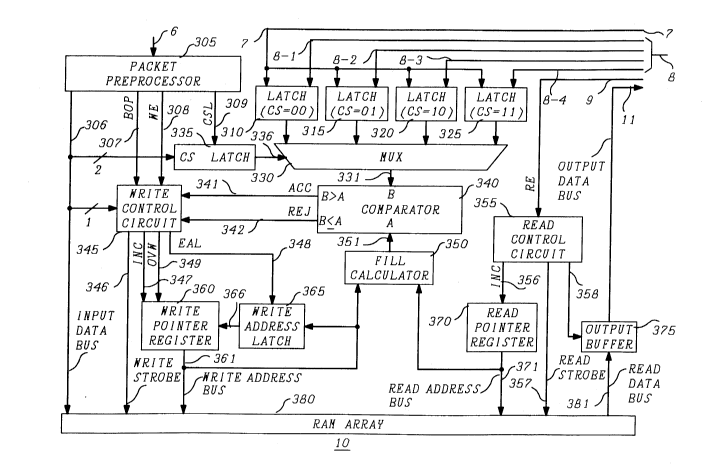
shown in FIG. 3.
In particular, preprocessor circuit 305 responsive to receipt of a
35 data byte via bus 6 checks the pattern of the bits contained therein to
determine if the bits conform with the pattern of the aforementioned F flag.
- 5 -
Preprocessor 305 discards the data byte if it finds that to be the case.
Otherwise, it temporarily stores the byte in a holding register (not shown)
contained in preprocessor 305. The data byte stored in the holding register
is the first byte of an incoming data packet, i.e., the first byte of the ADD
5 field. At this point, preprocessor 305 checks to see if bit 0 of the data byte is set, thereby noting the end of the ADD field.
Assuming that bit 0 is not set, then on receipt of the next data
byte, preprocessor 305 (a) outputs to bus 306 the data byte contained in the
holding register; (b) sets a BOP flag outputted to lead 307; (c) stores the
10 newly arrived data byte in the holding register; and (d) checks bit 0 of thatbyte to see if it denotes the end of the ADD field. Assuming that is the
case, then preprocessor 305 sets a flag so that it will identify the ~ext
incoming data byte that it receives as the K1 byte, and hence identify the
CS bits contained in that byte. Thus, preprocessor 305 temporarily stores
15 each data byte that it receives in the holding register and then outputs thatdata byte to bus 306 upon receipt of the next data byte. Preprocessor 305
continues in this manner until it receives the next F flag denoting the end
of the packet.
It is seen from the FIG. that BOP lead 307 extends to write
20 control circuit 345. Write control circuit 345 responsive to the assertion ofthe BOP flag on lead 307 outputs an enable address latch (EAL) signal to
lead 348 extending to write address latch 365. The EAL signal on lead 348
causes write address latch 365 to store in its internal register circuits (not
shown) the memory write address that appears on multibit bus 361. As will
25 be seen below, this action sets the stage for discarding the incoming packet
in the event that the packet's associated watermark threshold does not
exceed the number of RAM 380 memory locations that are filled following
the storage of the last of the packet's data bytes in ~2AM 380 (buffer
memory), which may be, for example, a so-called dual port RAM having
30 1024 memory locations of 12 bits each memory location.
The assertion of BOP lead 307 also causes write control
c;rcuit 345 to disregard the first data byte that preprocessor 305 outputs to
bus 306. Write control circuit 345 does this so that the address of packet
switch 10 is effectively "stripped off" the incoming data packet before the
35 latter is delivered to the next node in the data network. In fact, each
packet switch that is used to deliver a data packet to its final destination
2~9~3~
.
removes its address from the address field.
When packet preprocessor 305 outputs a data byte to multibit
bus 306 it also outputs a write enable (WE) signal to lead 308 extending to
write control circuit 345. Except in the case of the first data byte
5 identifying packet switch 10, write control circuit 345 responsive to the WE
signal increments write pointer register 360 via lead 347, thereby causing
the RAM 380 write address that register 360 outputs to multibit bus 361 to
increase by one. Write control circuit 345 then outputs to lead 346
extending to RAM 380 a write-enable strobe signal, thereby causing RAM
10 380 to store the data word appearing on bus 306 in the memory location
identified by the address on bus 361. Thus, except as noted above, write
control circuit 345 performs the foregoing each time preprocessor 305
outputs a data word to bus 306 and a write enable signal to lead 308.
Included in packet switch 10 is CS latch 335 which is used to
15 store a copy of the class-of-service (CS) bits when they appear on bus 306. It
is seen from the FIG. that two of the bit leads of bus 306 extend to CS latch
335. It is these bit leads which carry the CS bits when preprocessor 305
outputs the K1 byte to bus 306. At that time, preprocessor 305 also pulses
lead 309 extending to CS latch 335. CS latch 335 responsive to that pulse,
20 latches a copy of the CS bits into its two-bit register. CS latch 335 then
supplies the bits to multiplexer 330 via two-lead bus 336. The binary value
(00, 01, 10 or 11) of the CS bits is thus used to cause one of four watermark
thresholds stored in registers 310, 315, 320 and 325, respectively, to be
multiplexed via bus 331 to one input (B) of comparator 340.
Comparator 340 also receives at its other input (A) via bus 351
the number of RAM 380 memory locations that are filled, i.e, contain data
words which have not yet been read out of RAM 380. The number of filled
memory locations is determined by calculator circuit 350 using the well-
known technique of modulo subtraction operating on the binary value of the
RAM 380 write address appearing on bus 361 and the binary value of the
RAM 380 read address appearing on bus 371. The result of that calculation
is then outputted to bus 351.
Comparator 340, in turn, compares the watermark threshold
that it receives via bus 331 with the number that it receives via bus 351. If
35 the value of the threshold exceeds the number, then comparator outputs a
signal via lead 341 (ACC) as an indication that the data byte should be
2(~43~
_,
accepted. Otherwise, comparator 340 outputs a signal via lead 342 (REJ) as
an indication that the data word should be rejected (discarded). However, in
the illustrative embodiment of the invention, packet switch 10 does not
respond to either assertion until the last data word of the incoming packet
5 has been stored in RAM 380, as mentioned above.
In particular, when packet preprocessor 305 detects the end of a
packet in the manner described above, it appends a bit (EOP) to the last
byte of the CK2 field and then outputs the result to bus 30B. It is seen
from the FIG. that the bit lead of bus 306 which carries the EOP bit
10 extends to write control circuit 345. Write control circuit 345 responsive tothe trailing edge of the EOP bit and the assertion of the write strobe pulse
on lead 346 primes itself to receive the final result outputted by comparator
340 to either lead 341 or 342.
Specifically, write control circuit 345 allows the packet that was
15 just stored in RAM 380 to remain therein if comparator 340 outputs a signal
via accept lead 341. However, write control circuit 345 rejects the packet if
comparator 340 outputs a signal via reject lead 342. Write control
circuit 345 rejects (discards) the packet by transferring the contents of write
address latch into registers contained in write pointer register 360. Write
20 control circuit 345 does this by pulsing overwrite (OVW) lead 349 connected
to write pointer register 360. Write pointer register 360 responsive to the
pulse allows its register to be overwritten by the address priorly stored in
write address latch 365 and supplied to bus 366. In this manner, the
contents of write pointer register 360 is effectively returned to the address
25 that was contained therein just prior to the loading of the first data byte
(i.e., second byte of the ADD field) of the incoming packet in RAM 380.
A data packet stored in RAM 380 may be sequentially unloaded
therefrom word-by-word. Node controller 20 (FIG. 1) does this by sending a
read enable (RE) signal to read control circuit 355 via lead ~. Read control
30 circuit 355 responsive to that signal increments via lead 356 the address
contained in read pointer register 370. The value of the increment is, for
example, a binary one as represented by a pulse on lead 356. Thereafter,
responsive to the trailing of the RE signal on lead 9, read control circuit 355
outputs to lead 357 extended to RAM 380 a strobe pulse. Ram control
35 circuit 380 responsive to that pulse unloads and supplies to read data bus
391 the data byte stored at the location identified by the read address that
- 2~ 3
pointer 370 outputs to read address bus 371. Buffer 375 accepts the data
byte upon receipt of an enable signal from read control circuit via lead 358.
Buffer 375 then supplies the data byte to output bus 11. Thereafter, the
remaining data bytes of the packet are outputted to bus 16 responsive to
5 receipt of respective read enable signals from controller 20.
Turning now to FIG. 4, there is shown a functional block
diagram illustrating the relationship between the values of the class-of-
service bits and their respective watermark thresholds (WMT). As
mentioned above, the binary values of the class-of-service bits identify
10 respective priority levels in which the binary value 00 defines, for example,the lowest priority level---and in which the binary value 11 defines, for
example, the highest priority level. It is seen from the FIG. that the
priority levels 00 through 11 "point to" respective watermark thresholds
WMT 1 through WMT 4, as mentioned above. The numerical designations
15 310,315,320 and 325 associated therewith are the designations of the
registers shown in FIG. 3. A watermark threshold stored in one of those
registers defines, more or less, a RAM 380 fill level, as depicted by the
dashed lines shown in FIG. 4. For example, in a preferred embodiment of
the invention, the watermark threshold associated with priority level 11 has
20 a value of 1023.
As mentioned above, the watermark thresholds may be inputted
by a system administrator positioned at terminal 15. Central processor 25
responsive to receipt of the thresholds generates a system control packet
containing the (a) address of the node whose watermark thresholds are
25 being changed, for example, the node depicted in FIG. 1, (b) new value(s) of
the watermark thresholds(s), and (c) identity of the respective register 310,
315,320 and/or 325. The data packet is then delivered to controller 20 via
packet switch 10 and bus 6.
Upon receipt of the packet, controller 20 translates the address
30 of the register whose contents are to be changed, for example, register 310,
into one of four enable leads 8-1 through 8-4 connected to controller 20 via
multilead cable 8 (FIGs.1 and 3). Controller 20 then loads onto bus 7 the
new watermark threshold that is to be stored in that register and enables
the register's enable lead, i.e., lead 8-1. Register 310 responsive to the enable
35 signal on lead 8-1 accepts the data present on bus 7.
`- 20~ 3~
g
The foregoing is merely illustrative of the principles of the
invention. Those skilled in the art will be able to devise numerous
arrangements which although not explicitly shown or described herein,
embody those principles and are within its scope and spirit.