Note: Descriptions are shown in the official language in which they were submitted.
~ Q~450
DATA TRANSFERRING SYSTEM COMPRISING AN INPUT-OUTPUT
CHANNEL UNIT CAPABLE OF PREDICTING AN OVERRUN
IN A DATA PROCESSING DEVICE
Background of the Invention:
This invention relates to a data transferring
system for use in carrying out data transfer in a
steaming manner between a peripheral controller and an
5 input-output channel unit in a data processing device.
A data processing device of the type described,
comprises an interface between the peripheral controller
and the input-output channel. The interface comprises a
data line, a start informing signal line tnamely, an SCI
10 line~, a start informing acknowledgement signal line
(that is, an SEO line), a strobe pulse signal line (or,
an STI line), and a strobe pulse acknowledgement signal
line (namely, an STO line).
The peripheral controller comprises a control
15 circuit which comprises a strobe pulse signal generator
for producing a strobe pulse signal to deliver the
strobe pulse signal to the strobe pulse signal line.
2 ~ 4 5 Q
The control circuit further comprises a signal producer
for producing, during a preselected time interval, a
start code signal having a start code representative of
a start of the data transfer. The signal producer
5 produces a start informing signal of logic "1" level
during production of the start code signal. The start
informing signal is for use in informing the
input-output channel unit of production of the start
code signal. The signal producer delivers the start
10 informing signal to the start informing signal line.
Connected to the signal producer and the data line, a
first buffer memory periodically memorizes the start
code signal as a memorized code signal at a first period
which is determined by a strobe pulse acknowledgement
15 signal. The first buffer memory delivers the first
memorized code signal to the data line.
The input-output channel unit comprises a first
receiver connected to the start informing signal line
for receiving the start informing signal as a received
20 informing signal. Connected to the first receiver and
the start informing acknowledgement signal line, a first
transmitter transmits the received informing signal to
the start informing acknowledgement signal line as a
start informing acknowledgement signal to deliver the
25 start informing acknowledgement signal to the control
circuit. A register is connected to the data line and
the first receiver. Enabled by the received informing
~Q ~9450
signal, the register registers the memorized code signal
as a registered code signal.
Connected to the strobe pulse signal line, a
second receiver receives the strobe pulse signal as a
5 received pulse signal. A second transmitter is
connected to the second receiver and the strobe pulse
acknowledgement signal line to transmit the received
pulse signal to the strobe pulse acknowledgement signal.
A second buffer memory is connected to the data
10 line and to a main memory. The first and the second
buffer memory are for use in transmitting transfer data
between the main memory and a peripheral device
connected to the second buffer memory through the data
line under control of the strobe pulse signal and the
15 strobe pulse acknowledgement signal after transfer of
the start code signal.
In the data transferring system which carries
out the data transfer in a streaming method, each of the
strobe pulse line and the strobe pulse acknowledgement
20 line is not put into an interlock state when the
transfer data are transferred between the peripheral
controller and the input-output channel unit.
Therefore, when an overrun detecting circuit detects an
overrun in the input-output channel unit, the
25 input-output channel unit stops delivery of the strobe
pulse acknowledgement signal to the strobe pulse
acknowledgement signal line. The input-output channel
unit further informs the peripheral controller of
4 2~ fl9450
occurrence of the overrun. When the peripheral
controller is informed that the overrun occurs in the
input-output channel unit, the peripheral controller
carries out a command retry processing in which a
5 leading part of a transfer command memorized in the main
memory is again transferred from the main memory to the
peripheral controller.
The overrun mainly occurs in the input-output
channel unit due to shortage of a memory capacity of the
10 second buffer memory when access contention takes place
between the input-output channel unit and other
input-output channel units for the main memory.
Therefore, the input-output channel unit may
again start accessing for the main memory when a
15 predetermined time interval lapses after occurrence of
the contention. Inasmuch as the data transfer is
suspended or stopped by stopping delivery of the strobe
pulse acknowledgement signal from the input-output
channel unit to the strobe pulse acknowledgement signal
20 line when the overrun occurs, the command retry
processing which needs a long time should be carried
out.
When a small amount of the transfer data is
transferred between the input-output channel unit and
25 the peripheral controller, the data processing device is
almost not influenced. When the transfer data has a
long length, the data processing device is influenced in
the fol~owing manner.
2 0 Q ~ ~ 5 0
It will be assumed that the transfer data has an
8 MB (megabit) length and that the transfer data is
transferred at an effective transmission rate which is
equal to 3 MB per second. In this case, it is necessary
5 in general to finish the data transfer at a time
interval which is equal to 8/3 seconds. However, it is
necessary in a worst case to finish the data transfer at
another time interval of 16/3 seconds. Inasmuch as a
long time is waisted in the worst case, the data
10 processing system may be put into a system down state.
In order to inhibit the system down state of the data
processing device, the data processing device may be
provided with a specific signal transmission line
between the input-output channel unit and the peripheral
15 controller. Such provision of the specific transmission
line results in an increase of hardware of the data
processing device.
Summary of the Invention:
It is therefore an object of this invention to
20 provide a data transferring system which is capable of
preventing an overrun which occurs in an input-output
channel unit.
It is another object of this invention to
provide a data transferring system of the type
25 described, which comprises the input-output channel unit
capable of predicting the overrun in order to prevent
the overrun.
~00~450
It is still another object of this invention to
provide data transferring system of the type described,
which has a decreased hardware.
Other objects of this invention will become
5 clear as the description proceeds.
On describing the gist of this invention, it is
possible to understand that a data transferring system
is for use in carrying out data transfer between a
peripheral controller and an input-output channel unit
10 in a data processing device comprising a data line, a
start informing signal line, a start informing
acknowledgement signal line, a strobe pulse signal line,
and a strobe pulse acknowledgement signal line. The
peripheral controller comprises: strobe pulse signal
15 generating means for producing a strobe pulse signal and
for delivering the strobe pulse signal to the strobe
pulse signal line; signal producing means for producing,
during a preselected time interval, a start code signal
having a start code representative of a start of the
20 data transfer and for producing, during production of
the start code signal, a start informing signal for use
in informing the input-output channel unit of production
of the start code signal, the signal producing means
being for delivering the start informing signal to the
25 start informing signal line; and first memorizing means
connected to the signal producing means and the data
line for periodically memorizing the start code signal
as a memorized code signal at a first period determined
7 ~Q 0~50
by a strobe pulse acknowledgement signal and for
delivering the memorized code signal to the data line.
The input-output channel unit comprises: first receiving
means connected to the start informing signal line for
5 receiving the start informing signal as a received
informing signal; first transmitting means connected to
the first receiving means and the start informing
acknowledgement signal line for transmitting the
received informing signal to the start informing
10 acknowledgement signal line as a start informing
acknowledgement signal; registering means connected to
the data line and the first receiving means and enabled
by the received informing signal for registering the
memorized code signal as a registered code signal;
15 second receiving means connected to the strobe pulse
signal line for receiving the strobe pulse signal as a
received pulse signal; second transmitting means
connected to the second receiving means and the strobe
pulse acknowledgement signal line for transmitting the
20 received pulse signal to the strobe pulse
acknowledgement signal line as the strobe pulse
acknowledgement signal; and second memorizing means
connected to the data line, the second receiving means,
and a main memory. The first memorizing means is
25 connected to a peripheral device. The first and the
second memorizing means is for use in transferring
transfer data between the main memory and the peripheral
device through the data line after the registering means
2 0 ~\ ~ 4 5 0 ~
registers the memorized code signal. The first and the
second memorizing means is for memorizing the transfer
data as first and second memorized data at the first
period and a second period determined by the received
5 pulse signal.
According to this invention, the input-output
channel unit comprises: overrun predicting means
connected to the second memorizing means for predicting
occurrence of an overrun on the basis of an amount of
10 the second memorized data to produce an overrun
prediction signal. The first transmitting means is
connected to the overrun predicting means for
transmitting the overrun prediction signal to the start
informing acknowledgement signal line. The peripheral
15 controller comprises: strobe inhibiting means connected
to the start informing acknowledgement signal line, the
strobe pulse signal generating means, and the strobe
pulse signal line and responsive to the overrun
prediction signal for inhibiting delivery of the strobe
20 pulse signal to the strobe pulse signal line during a
predetermined time interval.
Brief Description of the Drawing:
Fig. 1 is a block diagram of a data processing
device comprising a data transferring system according
25 to an embodiment of this invention; and
Fig. 2 is a block diagram of a strobe inhibiting
circuit of the data processing device illustrated in
Fig. 1.
5 0
Description of the Preferred Embodiment:
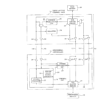
Referring to Fig. 1, a data transferring system
10 according to a preferred embodiment of this invention
is for use in carrying out data transfer between a
5 peripheral controller 11 and an input-output channel
unit 12 in a data processing device. Between the
peripheral controller 11 and the input-output channel
unit 12, the data processing device comprises a data
line 13, a start informing signal line 14, a start
10 informing acknowledgement signal line 15, a strobe pulse
signal line 16, and a strobe pulse acknowledgement
signal line 17. The start informing signal line 14, the
start informing acknowledgement signal line 15, the
strobe pulse signal line 16, and the strobe pulse
15 acknowledgement signal line 17 are called in the art an
SCI line, an SEO line, an STI line, and an STO line,
respectively.
The peripheral controller 11 comprises a control
circuit 18 comprising a strobe pulse signal generator 19
20 for producing a strobe pulse signal 20 to deliver the
strobe pulse signal 20 to the strobe pulse signal line
16 through a strobe inhibiting circuit 21 and a strobe
pulse signal driver 22. The strobe inhibiting circuit
21 will later be described. The control circuit 18
25 further comprises a signal producer 23 for producing,
during a preselected time interval, a start code signal
24 having a start code representative of a start of the
data transfer. The signal producer 23 produces a start
20 Q~50
informing signal 25 of logic "1" level during production
of the start code signal 24. The start informing signal
25 is for use in informing the input-output channel unit
13 of production of the start code signal 24. The
S signal producer 23 delivers the start informing signal
25 to the start informing signal line 14 through a start
informing signal driver 26.
Connected to the signal producer 23 and the data
line 13, a first buffer memory 27 periodically memorizes
10 the start code signal as a first memorized code signal
at a first period which is determined by a strobe pulse
acknowledgement signal 28. The first buffer memory 27
delivers the first memorized code signal to the data
line 13 through a data driver 29.
The input-output channel unit 12 comprises a
first receiver 30 connected to the start informing
signal line 14. The first receiver 30 receives the
start informing signal 25 as a received informing
signal. Connected to the first receiver 30 through an
20 OR circuit 31 and to the start informing acknowledgement
signal line 15, a first transmitter or driver 32
transmits the received informing signal to the start
informing acknowledgement signal line 15 as a start
informing acknowledgement signal to deliver the start
25 informing acknowledgement signal to the control circuit
18 through a start informing acknowledgement signal
receiver 33. A register 34 is connected to the data
line 13 through a data receiver 35 and to the first
~0 ~50
receiver 30. Enabled by the start informing signal 25,
the register 34 registers the first memorized code
signal as a registered code signal.
Connected to the strobe pulse signal line 16, a
5 second receiver 36 receives the strobe pulse signal 20
as a received pulse signal. A second transmitter or
driver 37 is connected to the second receiver 36 and the
strobe pulse acknowledgement signal line 17. The second
transmitter 37 transmits the received pulse signal to
10 the strobe pulse acknowledgement signal line 17. A
strobe pulse acknowledgement signal receiver 38 receives
the received pulse acknowledgement signal as the strobe
pulse acknowledgement signal 28.
The input-output channel unit 12 further
15 comprises a second buffer memory 39 connected to a main
memory 40 and to the data line 13 through the data
receiver 35. The second buffer memory 39 is connected
through another data transmitter or driver 41 to the
data line 13 which is connected to the first buffer
20 memory 27 through another data receiver 42.
An inhibit gate circuit 43 is connected to the
first and the second receivers 30 and 36. The inhibit
gate circuit 43 inhibits delivery of the received pulse
signal to the second buffer memory 39 when receives the
25 received informing signal of logic "1" level from the
first receiver 30. When the received informing signal
becomes to have a logic "0" level after the first
memorized code signal is registered in the register 33,
12 ~ ~ Q~50
the inhibit gate circuit 43 delivers to the second
buffer memory 39 the received pulse signal delivered
from the second receiver 36.
The strobe inhibiting circuit 21 is connected to
5 the signal producer 23 and the start informing
acknowledgement signal receiver 33.
On transmitting the start code signal 24 from
the peripheral controller 11 to the input-output channel
unit 12 through the data line 13, the strobe inhibiting
10 circuit 21 receives the start informing signal of logic
"1" level and the start informing acknowledgement signal
of logic "1" level. On reception of the start informing
signal of logic "1" level and the start informing
acknowledgement signal of logic "1" level, the strobe
15 inhibiting circuit 21 never inhibits delivery of the
strobe pulse signal 20 to the strobe pulse signal line
16 in the manner which become clear as the description
proceeds.
When such transferring operation of the start
20 code signal 24 comes to an end, each of the start code
signal line 14 and the start code acknowledgement signal
line 15 becomes to have a logic "0" level. In this
case, the strobe inhibiting circuit 21 also never
inhibits delivery of the strobe pulse signal 20 to the
25 strobe pulse signal line 16 in the manner which will
later become clear. As a result, it is possible to
carry out the data transfer between the input-output
5 0
13
channel unit 12 and the peripheral controller 11 in the
following manner.
The first buffer memory 27 is connected to a
peripheral device 44. The first and the second buffer
5 memories 27 and 39 are for use in transferring transfer
data between the main memory 40 and the peripheral
device 44 through the data line 13 after the register 34
registers the memorized code signal. The first and the
second buffer memories 27 and 39 are for memorizing the
10 transfer data as first and the second memorized data at
the first period and a second period determined by the
received pulse signal.
Connected to the second buffer memory 39, an
overrun predicting circuit 45 predicts occurrence of an
15 overrun with reference to an amount of the second
memorized data to produce an overrun prediction signal
46 of logic "1" level. More specifically, the overrun
predicting circuit 45 produces the overrun prediction
signal 46 when the amount of the second memorized data
20 is increased up to an upper threshold amount and when
the amount of the second memorized data is reduced to a
lower threshold amount which is lower than the upper
threshold amount. Each of the upper and the lower
threshold amounts is decided in consideration of an
25 amount of the transferred data carried on the data line
13.
The overrun prediction signal 46 of logic "1"
level is delivered to the strobe inhibiting circuit 21
14 ~ 4 5 0 ~
through the OR circuit 31, the first transmitter 32, the
start informing acknowledgement line 15, and the
receiver 33. Responsive to the overrun prediction
signal 46 of logic "1" level, the strobe inhibiting
5 circuit 21 inhibits delivery of the strobe pulse signal
to the strobe pulse signal line 16 during a
predetermined time interval which is described in the
preamble of the instant specification.
Referring to Fig. 2, the strobe inhibiting
10 circuit 21 comprises a delay circuit 47 connected to the
receiver 33. The delay circuit 47 delays the overrun
prediction signal 46 (Fig. 1) by a delay equal to the
predetermined time interval to produce a delayed
prediction signal of logic "1" level. Responsive to an
15 inverted signal of the delayed prediction signal, the
overrun prediction signal 46, and an inverted signal of
a logic "0" level signal, an NAND circuit 48 produces an
NANDed signal. Responsive to the NANDed signal and the
strobe pulse signal 20, an AND circuit 49 produces an
20 ANDed signal. With this structure, the strobe
inhibiting circuit 21 inhibits delivery of the strobe
pulse signal 20 to the strobe pulse signal line 29 in
response to the overrun prediction signal 46.