Note: Descriptions are shown in the official language in which they were submitted.
~t' ~J ~%'~d59L8
This invention relates to spin-on glass, and more
particularly to a method of applying cumulative thick layers
of spin-on glass, especially inorganic or quasi-inorganic
spin-on glass, to a substrate without cracking.
Spin-on glasses (SOGs) are proprietary liquid
solutions containing siloxane or silicate based monomers
dissolved in various kinds of solvents or alcohols. During
coating and curing, monomers are polymerized by condensation
and release water, alcohol and other solvents.
l0 The cured material is a thin solid film having
mechanical, chemical and electrical properties that depend on
the starting solution, and the coating and curing process.
A primary use of SOGs is in the planarization of
dielectrics in the fabrication of semi-conductor devices. As
will be explained in more detail below, in the fabrication
process trenches are formed in the dielectric layer.
Especially at high packing densities it becomes important to
fill in these layers to provide an even surface, a process
known as "planarization".
Among many of the dielectric planarization
techniques, SOG planarization is a particularly attractive
method; it is relatively simple, economical and is capable
of high throughput. SOG planarization is used over
polysilicon, refractory metals, polycides, silicides,
aluminum and aluminum alloys, copper, and gold, where the
main goal is to smooth or eliminate steps in the surface and
enhance step coverage by the dielectrics and interconnects.
SOG planarization can take three farms:
1) Complete etchback.
2) Partial etchback.
3) Non etchback.
- Z -
~.C'~Cr'~~~g
Major manufacturing restrictions of the
complete/partial etchback techniques impose the non-etchback
approach as tape preferred one in a production environment.
In this approach, SOG becomes a permanent part of
the dielectric. Film properties are then of prime
importance. Since SoG is generally a more porous material,
when compared to LPCVD, APCVD, LACVD, PhACVD or PECVD oxides,
it is more prone to water absorption. This water absorption
reduces the bulk resistivity of the SOG and increases the
power consumption of the semiconductor device due to current
leakage between adjacent tracks of the same level of
interconnect. For this reason, among others, SOG does not
contact directly these tracks and is sandwiched between two
denser LPCVD, APCVD, LACVD, PhACVD or PECVD dielectric films.
Interconnections are required between the upper and
lower tracks, requiring the use of contacts or vias, and the
SOG is then in direct contact with the interconnects at those
locations. If too much water is present in the SOG, problems
such as via poisoning can occur.
2.0 There are more than one hundred different SOG
solutions on the market. These are classified in two major
families:
~ Quasi-inorganic SOGs
- Siloxanes (methyl-, ethyl-, phenyl-,
butyl-, doped or undoped)
~ Purely-inorganic SOGs.
- Silicates (doped or undoped)
Purely inorganic silicate SOGs are prone to severe
cracking. The quasi-inorganic siloxane SOGs have a more
flexible structure due to the presence of some organic
radicals which prevent complete cross-linking of the SiOXCyHZ
matrix under condensation. The flexible structure reduces
..
P ",
the tendency of an organic SOG to crack, but unfortunately
the presence of the hydrogen atoms in the quasi-inorganic
SOGs impairs the dielectric properties and essentially rules
them out for use in sensitive CMOS devices.
Furthermore, the organic radicals are not stable at
high temperatures and are not compatible with oxygen plasma
photoresist strippers, which tend to transform the quasi-
inorganic SOG to an purely inorganic SOG by burning the
organic bonds and producing volatile compounds like H2o,
.. COxHy, and silanol Si-OH. While inorganic SOGs are
preferred, which are not degraded by the photoresist
strippers, the cracking problem has imposed severe
restrictions on layer thickness and thus the degree of
planarization that can be achieved.
Planarization technology becomes increasingly
important when the scale of integrated circuits shrinks to
micron and sub-micron region.
Various techniques have been proposed to reduce
cracking in inorganic SOG layers, but in all cases the
maximum thickness of the crack-free layer obtainable is
severely limited. U.S. Patent No. 4,801,560 to Motorola
discloses that a thicker glass layer can be obtained by
depositing the spin-on glass in multiple layers separated by
chemical vapour deposition oxide. This patent suggests that
up to 30,000 Angstroms of glass can be deposited between the
layers as opposed to 4,000 Angstroms previously attainable.
However, the patent relates exclusively to carbon-containing,
or quasi-organic Sots. The patent states that without the
carbon, the spin-on glass layer becomes highly stressed and
easily cracked, and further states that without carbon it is
not possible to form a multi-layer structure as the layers do
not bond adequately together.
An object of this invention is to permit the
- 3 -
CA 02009518 2000-03-06
formation of thick spin-on glass layers, particularly
inorganic spin-on glass layers, with reduced cracking.
According to the present invention there is
provided an in-line method of planarizing a substrate with a
metallic interconnect layer formed thereon, comprising
sequentially depositing a plurality of spin-on glass
component layers on the substrate to form a composite
planarization layer, the spin-on glass component layers
comprising a mixture of a silanol polymer (SiXOy(OHPZ) or an
l0 organosilanol (SiWOx(OH)y(OC2H5)Z), phosphorus organometallic
catalyst (PWOX(OH)y(OR)Z), water, and a mixture of alcohols,
each component spin-on glass layer being subjected to in-
line heat treatment at a temperature of 300°-425°C. prior to
application of the next component layer for a time, which is
in the order of 60 seconds, that is just sufficient to
15 connect the organometallic catalyst and reduce residual
carbon atomic concentration after connection of the
organometallic catalyst to less than 1~ without destroying
the underlying interconnect layer.
20 The invention is particularly applicable to
inorganic spin-on glasses, which are preferred in semi-
conductor applications and for which the cracking problem is
most severe. Surprisingly, the invention allows composite
crack-free inorganic layers of 10,000 Angstroms or more to be
formed. This is as the result of the catalyst connection and
complete elimination of residual volatile solvents prior to
25 the application of an overlying layer, which surprisingly
occurs if the spin-on glass layer is heated to a temperature
of at least 300°C, and preferably at least 350°C.
While the invention can be most usefully applied to
inorganic spin-on glasses, it can also be applied
3o beneficially to quasi-inorganic spin-on glasses, where
improvement in the adhesion between the layers will occur.
- 4 -
CA 02009518 2000-03-06
Although spin-on glass can be applied for many
purposes, the primary use of the invention is in the
planarization of dielectric layers in semi-conductor devices,
including CMOS devices.
Another aspect of the invention provides a device
having a spin-on glass layer, wherein the spin-on glass is
inorganic or quasi-inorganic and said spin-on glass layer
comprises a composite layer of thickness t consisting of n
15
- 4a -
contiguous thin layers, each having a thickness of
approximately t/n.
The invention will now be described in more detail,
by way of example only, with reference to the accompanying
drawings, in which:-
Figures la to lh show the various stages in the
fabrication of a semi-conductor device with a conventional
planarization layer;
Figure 2a shows a planarized device with reduced
line spacings, showing crack formation in the SOG layer;
Figure 2b shows a wafer similar to Figure 2a with a
composite SOG layer in accordance with the invention:
Figure 3a shows a 200 nm. single SOG layer;
Figure 3b shows a 210 nm. composite SOG layer
consisting of three 67 nm. thin layers; and
Figure 4 is a chart of a differential thermal
analysis experiment performed to identify the temperature
required to connect the organometallic catalyst material,
densify the network, and evaporate the volatile by-prducts
such as ethanol.
Referring to Figures la to 1h, in a conventional
planarization process a first layer of interconnect material,
preferably aluminum, 1 (Figure la) is deposited on a
substrate 2 and etched away to expose tracks 1a, 1b (Figure
1b). A layer of dielectric 3 (which can be LPCVD, APCVD,
LACVD, PhACVD, PECVD, for example) is applied over the tracks
la, lb (Figure lc) and planarized with a spin-on glass layer
4 (Figure 1d). This planarization with a spin-on glass layer
is typically done with a dedicated SAG processor as follows:
- 5 -
(i) The wafer is transported from a sending
cassette to a coating chamber.
(ii) A few ml of a SOG solution is dispensed at the
centre of the wafer.
(iii) The wafer is spun at a given RPM to spread the
solution uniformly and permit volatile
compounds evaporation and film solidification.
(iv) The wafer is sequentially transport to in-line
hot plates for in-line cures at relatively low
temperature, typically lower than 250°C.
(v) The wafer is stored in a receiving cassette.
(vi) When all the wafers have been received in the
receiving cassette, they are sent together for
high temperature treatment, typically higher
than 425° to 450°C.
A second dilectric layer 5 is applied (Figure 1e)
and contact holes 6 (Fig. 1f) are formed in the dielectric
layers 3, 5 to expose the tracks la, 1b (Figure 1f). A
second layer of interconnect material 7 is deposited on the
resulting structure (Figure 1g), and the intervening material
of the second level of interconnect etched away to form the
finished interconnect tracks 7a, 7b.
As will be seen in Figure 1h, the planarization is
not perfect due to the limitation on the possible thickness
of the SOG layer 4. At wider line spacings, such as is shown
in figure 1h, incomplete planarization can be tolerated.
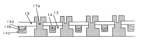
Figure 2a shows a high density device, which
employs narrower line spacings. Aluminum tracks 17a, 17b,
17c, 17d are separated by dielectric layers 13, 15 planarized
with SOG layers 14. Unfortunately, the formation of cracks
8 in the deeper SOG layers 14, due to surface tension and
capillary effects, has limited the application of this
technique to such high density devices.
~~'r~;i~l.~3
Since the second layer of dielectric is deposited
directly over the cured SOG, good planarization requires a
high viscosity SoG solution, and this implies the
accumulation of a very thick SOG layer in the valleys.
During the high temperature cure, film contraction occurs,
film stress increases, and cracking results.
To prevent this cracking problem, a very flexible
and high carbon content quasi-inorganic SOG has been tried,
but this technique has proved unacceptable because of an
important field inversion problem due to the effect of the
hydrogen contained in the organic bonds of the quasi-
inorganic SOGs on the characteristics of the CMOS
semiconductor devices, and such SOGs cannot be used in CMOS
devices. As a result there has been a tendency to avoid SOG
planarization altogether in these devices despite its
inherent advantages.
It has been found that, surprisingly, the cracking
problem that occurs, especially within inorganic SOGs, can be
eliminated by forming a multi-layer composite structure
provided that each layer of the composite structure is heated
0 0
to at least 300 C, and preferably at least 350 C prior to the
application of the next layer. The reasons for this are that
after the application of each coat, the organometallic
catalyst is connected, volatile by-products of that
connection can evaporate and mutual bonding of the layers is
enhanced by the absence of solvents, such as water and
alcohols, which could be released during the final curing
process. If a subsequent layer is applied with these
substances absent in the underlying layer it is possible to
form a coherent composite structure because internal volatile
pressuriztion does not occur and the layers become well
bonded together.
In Figure 2b the composite SOG layer 14, which is
210 nm. thick, consists of three thin layers 14a, 14b, 14c,
_ -r
~~~'~~J1~
each 67 nm. thick. The SOG solution applied in the
planarization step is a phosphorus doped SOG solution. This
is a mixture of a silanol six,0y(OH)z, or an organosilanol
polymer, SiwOx(OH)y(OC2H5)z, a phosphorus organometallic
polymer of PwOx(OH)y(OR)z, water, and a mixture of alcohols,
R-oH. This solution is stable when contained in a sealed
bottle.
After dispensing and spinning, the alcohols and
water evaporate and this permits the formation of a very
porous solid by silanol condensation which results in more
water formation:
SiOH H HOSi Si (H20) HOSi
O O O O O O
Si. O SiOH + HOS'i -> Si O Si O Si
O O O O (H20) O (H20) O
Si O SiOH HOSi Si O Si O Si
This porous solid then contains dissolved water,
alcohols and the not-yet-bonded phosphorus organometallic
compound. The wafer coated with this porous solid is
normally sequentially~transported to in-line hot platES for
the evaporation of the alcohols and water.
Chemical bonding between the phosphorus
organometallic compound and the porous solid does not
normally occur during this heat treatment with the in-line
hot plates because typical in-line temperature is limited to
about 250°C.
When exposed to higher temperature (>400°C), the
phosphorus organometallic molecule connects to the porous
solid and causes a substantial volumetric shrink,
densification, and the formation of water, H20, and alcohols,
g _.
~~~~J1~
such as ethanol, C2H50H. This process can be represented as
follows:
H
O Si. O Si O H
O
O O H
H
O
O Si O Si O H + H P : ->
O
C
C
O
O O H O
H
O Si O Si O H H
(H20)
O S1 O S1
O O O
H H
O Si O Si O + H C C O
P: O H
O O O H H
O Si O Si
(Ha0)
The liberation at this stage of a large and highly
volatile molecule such as ethanol in this densifying porous
solid is responsible for the generation of a high stress in
the solid. Gas pressure increases in the closing pores due
to the high temperature used and volatility of these by-
products.
The pressurization of the layer is not homogeneous
due to the fact that it is harder for the ethanol produced at
the bottom to diffuse over the larger distance to reach the
surface and escape. The stress is then larger at the bottom
of the layer.
This ethanol diffusion from the bottom of the layer
is particularly difficult because the surface of the film
densifies faster than its interior; the thicker the film the
~Cr'~591.8
more difficu7.t the ethanol diffusion up to the surface and
the more difficult the crack prevention becomes.
When the internal pressurization causes a local
mechanical stress which exceeds the mechanical strength of
the solid, cracks form and propagate.
During high temperature exposure, water and ethanol
must diffuse through the solid layer up to the surface from
which it will evaporate. Diffusion theory states that:
d - (Dt) ',
where d is the thickness of the layer and t is the curing
time. The time required to reach the surface is therefore
proportional to the square of the film thickness:
t - Dd2
By using multiple thin layers, instead of a single
thick layer, the elimination of dissolved water and alcohol
is much easier, and cracking can be eliminated. For example,
if instead of using a single d = 200 nm SOG layer, three
layers having a thickness d' of 67 nm are used, and if a
complete SOG cure is carried between each application, the
time t' required to eliminate the dissolved water and
alcohol, per coat, is:
t~ _ D(dv)2 _ D(d/3)2 _ D(d)2/9 _ t/95
if three coats are applied, the total required time is 3t' _
t/3. By using multiple thin coats, the SOG cure can be
greatly improved. In fact, if the curing time per coat, t',
is kept equal to the full curing time, t, a dryer and higher
quality SOG film is obtained, larger cumulative thickness is
possible, and tighter IC geometries are achievable. Three
layers have been described, but the larger the number of
coats, the better the final result and crack prevention.
~(J43~~~,~
EXAMPLE
A test structure was made as illustrated in Figure
2b with various photolithographically patterned aluminum
lines and spacings. Three 67 nm layers of TOK OCD-2P-37313-
SG, 4.0 wt% P205 SOG were applied, with each layer cured at
350°C for a time sufficient to eliminate the dissolved water
and alcohol. In this case t' = 60 seconds per coat, and the
overall time 3t' was 180 seconds.
As shown in Figure 3b, the resulting composite SOG
layer was crack free.
COMPARISON EXAMPLE
A single 200 nm SOG layer was formed on an
identical structure as shown in Figure 2a. The SOG layer
consisted of TOK OCD-2P-80327-SG, 4.0 wt% P205 SOG. A single
cure of 60 seconds was carried out after the layering in
accordance with prior art practice. The wafer was then split
so as to cleave the SOG, and cracks were observed as shown in
Figure 3a.
In order to determine the temperature needed to
2o ensure organometallic catalyst connection, volatile by-
product evaporation between each coat and then adequate
bonding between the multiple SOG layers, a gravimetric-
calorimetric Differential Thermal Analysis (DTA) experiment
was carr~_ed out to identify the temperature at which
connection of the organometallic material in the SOG to the
porous self matrix occurred. The SOG used was OCD-2P-37313-
SG.
Figure 4 is a chart showing the results.
For such DTA analysis some SOG solution was dried
at a temperature of 140~C for about three hours, cooled in
11
room air for many hours, and installed in the DTA apparatus.
Tts temperature was raised from 25°C to 1000°C at a fixed
rate of 10°C/min. The upper curve represents the weight loss
of a SOG film and the lower curve shows the heat loss/gain of
the SOG as its temperature is increased.
The low temperature endothermic peak associated
with a 10.00% weight loss shows that a quite large quantity
of absorbed gas is released from the open pores at low
temperature (62°C); This is mainly moisture and ethanol.
The high temperature (327°C) peak associated with a l6.Oo
weight loss is the peak of interest. It corresponds to the
connection of the phosphorus organometallic molecule to the
porous network, to volumetric contraction and to ethanol
connection by-product evaporation. This graph indicates that
a temperature of about 350°C is needed to connect the
organometallic, densify the matrix, and evaporate the newly
formed ethanol by-product.
Temperatures as low as 300°C can be used, but 350°C
is preferred to ensure good connectivity densification and
evaporation.
The confirmation of total ethanol elimination was
done by means of nuclear analysis:
Elastic Recoil Detection (ERD) using high energy
(30 MeV) 35C1 ions, mylar absorber, and time of flight (TOF)
analyzer can easily detect light elements such H and C in
thin films. This technique was used to analyze and compare
the SOG films obtained after in-line cure on the SOG
processor and after high temperature cure in a controlled
oven.
For the SOG used, the presence of the phosphorus
organometallic molecule was detected by the carbon present in
its ethoxy group. This carbon content (limit of detection
1? _
~~~'r~;~~..~
less than 0.01 atomic %) was about 2.0 atomic %. If the
molecule connects to the solid, its ethoxy group forms
volatile ethanol and the carbon content is reduced. The
lower the carbon content, the better the confirmation of the
organometallic molecule connection (the better crack
prevention).
A 67 nm film was coated and cured in-line with a
hot plate at 350 C to permit ethoxy group connection and
volatile ethanol formation. Another coat of the same
thickness was applied and cured the same way. Finally, a
third identical coat was applied and cured. The three coat
sandwich (200 nm) was then heated in a two-step high
temperature oven in nitrogen at a temperature not exceeding
425 C (noted as high T #1 and high T #2), and analysed. The
measured atomic concentrations were as given below:
PROCESS STEP C H N O Si P
after in-line <0.0 10.48 <0.0 61.88 26.8 00.83
cur
at 350 C
after high T #1 <0.0 10.38 00.04 61.54 27.3 00.73
after high T #2 <0.0 10.38 00.04 61.71 26.8200.64
It can be seen that the phosphorus is present after
the in-line cure but no carbon is detected. The phosphorus
organometallic molecule's ethoxy groups, -C2H5, became cross
linked with the densifying solid's silanol groups, Si-OH, to
permit the connection of the phosphorus and the generation of
volatile ethanol, C2H50H, which escaped completely from the
solid.
The comparison of the carbon and hydrogen
composition after "in-line cure", after "high T #1" and
after "high T #2", shows that the volatiles that could cause
film cracking were already removed after the in-line cure of
the three coats on the SOG processor due to the in-line 350 C
~~~~J1~
hot plate. This result is extremely important.
Undesirable residual hydrogen is bound to silicon
and phosphorus though oxygen to form -Si.OH and P.OH
radicals.
Although the invention is especially applicable to
inorganic SOGs, since it is inorganic SOGs that cause the
most severe cranking problems and inorganic SOGs that are
most desirable for planarization layers in CMOS devices, the
invention can be beneficially applied to quasi-inorganic SOGs
to reduce cracking and permit organic volatile by-products to
be reduced.
The number of thin layers can be varied. As a
general rule, the great the number of layers, the better the
end results.
The SOG layers can be heated with in-line high
temperature hot plates, or alternatively an in-line oven, an
in-line plasma cure device, an in-line microwave device, or
an in-line ozone device, or an in-line UV-ozone device, to
permit connection of the catalyst and elimination of the
organic by-products. The important point is that the
volatile substances are eliminated between the application of
each SOG layer.
While the invention has primarily been described in
connection with the planarization of dielectric layers in the
fabrication of integrated circuits, it can be applied in
other fields, namely:
To other steps in the manufacturing of IC's:
Planarization
Diffusion source
. Dielectric Layer
Diffusion Barrier
Encapsulation
Adhesion Layer
Buffer layer
1~
Antireflective layer
Corrosion protection layer
Etc...
To other semiconductor devices:
. Emission diodes
Liquid crystal display
Electro chromic display
Photodetectors
Solar batteries
. Sensors
To other fields:
Optical fibers
Corrosion protection
Adhesion promoters
. Friction reduction
Optical/thermal reflectance adjustments
_ ~r~ _