Note: Descriptions are shown in the official language in which they were submitted.
2009744
This invention relates to the field of semiconductor microprocessors,
particularly those processors which are able to access data in an external
memory.
~CKGROUND OF THE INVENTION
The present invention covers a pipelined floating-point load
instruction which may be implemented within the bus control unit of a
microprocessor. The microprocessor utilized with the present invention is
the Intel 860TM Microprocessor, frequently referred to as the N10TM
processor. (Intel is a registered trademark of Intel Corporation).
The N10 processor is a 32/64-bit IEEE compatible floating-point
processor, a 32-bit RISC integer processor and a 64-bit 3-dimensional
graphics processor. Using a numerics processor optimized for both vector
and scalar operations, it represents the industry's first integrated high
performance vector processor incorporating over one million transistors and
providing about 112 of the performance of the Cray1, all on a single chip.
All processors have some form of load instruction that can access
information from either an external memory or an internal data cache.
Access to externally stored data is usually made via an external data bus
controlled by the internal logic of the processor. The rationale of using a
data cache is to provide efficient access to frequently used information,
thereby accelerating processing speed. In processors that utilize a data
cache, normal load instructions will operate most efficiently if the data
information is resident fn the onchip cache. That is, if the data is not In
the
cache there is a penalty in performance when axessing the data.
Typically, when external data is referenced using a normal load
1
2009744
instnrction it is stored in the cache. The reason for this is that, under
normal
conditions, data which has just been referenced is very likely to be
referenced again in the near future. The data access penalty is minimized
by providing the most frequently accessed information in the internal data
cache while reserving external memory for seldomly referenced or reused
information. It is the principle of locality which makes the data cache a
useful tool since programs tend to reference certain data repeatedly in the
- near future.
A problem arises however, when a processor is required to deal with
very large data structures or, in any event, data structures that are much
bigger than that which the data cache can normally hold. As an illustration
of the difficulty that can arise, a processor is often required to perform a
variety of floating-point operations, such as matrix inversion,
multiplication,
etc., which require manipulation of huge data matrices. In prior art
processors when the data is not in the onchip data cache, the processor
must freeze execution and request access from external memory. During
the time that execution is frozen, the processor is prevented from issuing
any new addresses to memory. In other words, the processor must wait for
the data for the first operation to arrive from external memory, before
continuing its operations. As a result, this type of access to external
memory can take six clock cycles or longer. Thus, a substantial delay is
introduced into the processing speed of the system when frequent access to
external memory is mandated by the size of the data structures involved.
Another problem related to the handling of large data structures
arises when the externally accessed data is brought into the processor. As
external data is delivered to the processor, it is written into the cache --
usually replacing previously resident data. However, it should be
remembered that some external data (most commonly in the case of large
data structures) is infrequently referenced information, Le., it is not
expected
to be reused, while the replaced data in the cache is information that is very
likely to be referenced repeatedly in the near future. Therefore, the
2
''"~ 2009744
processor is tossing out data that needs to be reused in favor of data that
will in all likelihood only be referenced once. As a consequence, an
inordinate amount of time is spent recalling the replaced cache data. This
increased accessing time is another reason why prior art processors run at
a much slower rate than is achieved by the present invention.
As will be seen, the present invention implements a pipeline structure
which is capable of processing memory operations at a much faster rate
(essentially at the full bus bandwidth) without any delay of waiting for the
processor to generate the next address. By using this pipelined structure,
the processor associated with the present invention can continue issuing
addresses without having to wait for the arrival of the data from external
memory. This capability enhances the presently described microprocessor
when compared to prior art processors.
To achieve this performance, the present invention provides a
pipelined floating-point load instruction to rapidly access data stored in
external memory. This pipelined floating-point load software instruction,
which is more easily referred to as "PFLoad" or "PFId", may be used by a
programmer to access data which is stored either in the onchip data cache
or in an external memory system. The instruction is optimized for the
situation in which the data is not already residing within the processor's
internal data cache. This situation is referred to as a "cache miss" or,
phrased alternatively, a "PFLoad miss". The opposite casein which the
data that is to be loaded is already stored within the data cache -- called a -
"cache hiY -- is also handled by the present invention.
Additionally, the PFLoad instruction of the present invention does not
replace data already resident within the data cache, but rather directs the
newly accessed data to a storage location within the floating point unit of
the processor. The PFLoad instnrction will be discussed in conjunction
with its current implementation in the bus control unit of the N10 processor.
3
''~' 2009744
A specialized microprocessor instruction optimized for accessing
floating-point data stored in an external memory system is described. The
invention utilizes the pipelined architecture of the microprocessor to
efficiently retrieve external data that is unlikely to be reused again in the
near future; transferring the data directly to a floating-point data latch.
Frequently referenced data resident in the onchip data cache remains
undisturbed.
The pipelined floating-point load instruction of the present invention
includes a first-in-first-out (FIFO) memory for accumulating the accessed
data. In conjunction with the FIFO, a first circuit means is provided for
delivering the data from external memory to the FIFO, and a second circuit
means is provided for transferring the data from the FIFO to the floating-
point data latch. The second circui! means also couples data from the data
cache back to the FIFO in the event of a cache hit (i.e., the referenced data
actually resides in the data cache). Finally, a bus control means is
provided, coupled to the first and second circuit means, for controlling the
pipelined flow of data from the external memory system to the floating-point
unit.
One object of.bpresent invention is to provide a pipe~ned
instruction which is capable of processing memory operations at a much
faster rate than prior art processors. As such, the present invention can
continue issuing addresses without having to wait for the arrival of the
actual data from external memory.
Another object of the present invention is to provide access to
external data without replacing data already resident in the onchip data
cache. By doing so, the present invention minimizes total accessing time;
thereby increasing operation speed.
A further object of the present invention is to provide an efficient and
fast means for handling arithmetic operations involving very large data
4
2009744
structures.
Accordingly, in one of its aspects, the present invention resides in a
microprocessor having a pipelined architecture, a data cache coupled to a
floating-point unit along an internal bus, and a bus control unit which
controls access to an external memory along an external bus, an apparatus
for controlling the pipelined loading of floating-point data in said
microprocessor comprising: a first circuit means for storing floating-point
data in a pipelined manner as it is received from said external memory; a
bi-directional bus coupling said first circuit means to said internal bus,
said
.bi-directional bus transferring the floating-point data stored in said first
circuit means to a floating-point data latch via said internal bus; and
control
means for controlling said first circuit means and said data cache so that
floating-point data previously stored in said first circuit means may be
pipelined to said floating-point data latch without contention of said
internal
bus by said data cache, and further wherein floating-point data received by
said first circuit means is not otherwise written into said data cache.
In a further aspect, the present invention resides in a processor
having a pipelined architecture, a data cache coupled to a floating-point unit
along an internal bus, and a bus control unit which controls access to an
external memory along an external bus, and apparatus for controlling the
pipelined loading of floating-point data into said processor comprising: a
first buffer coupled to said external bus for receiving floating-point data
from
said external memory; a first circuit means for storing floating-point data in
a pipelined manner as it is received from said external memory by said first
buffer; a first bus coupled to said first circuit means and to said internal
bus
for transferring the floating-point data stored in said first circuit means to
a
5
B
-.., 200 9~4~
floating-point data latch in the event of a cache miss; a second bus
coupling said data cache to said first circuit means such that floating-point
data residing in said cache is returned to said first circuit means when a
cache hit occurs; and a control means for controlling said first buffer, said
first circuit means, said first, second and internal buses, and said data
cache such that floating-point data received from said external bus is not
written directly into said data cache, but wherein floating-point data
previously stored in said first circuit means is pipelined to said data latch
along said first and internal buses without contention of said internal bus by
said data cache when a cache miss occurs, floating-point data being
returned to said first circuit means from said data cache along said second
bus in the event of a cache hit.
In a still further aspect, the present invention resides in a processor
having a floating-point unit, a data cache and a port to an external memory
system, a method for pipelined accessing of floating-point data elements
from said external memory, said method being executable by instruction
means within said processor, said method comprising the steps of: issuing
an address to a floating-point data element resident within said external
memory; writing a previously addressed floating-point data element from
said external memory to an N-stage, first-in-first-out (FIFO) memory, where-
N is an integer greater than 1, said FIFO memory storing a Nth previously
addressed data element; reading said Nth previously addressed floating-
point data element from said FIFO memory to a bus; transferring said Nth
previously address floating-point element from said bus to a data latch
within said floating-point unit.
5a
u:
2009744
The present invention will be understood more fully from the detailed
description given below and from the accompanying drawings of the
preferred embodiment of the invention, which, however should not be taken
to limit the invention to the specific embodiment but are for explanation and
understanding only.
Figure 1 illustrates the logical partitioning of the processor
associated with the pipelined floating-point load instruction of the present
invention.
Ftgure 2 shows the currently preferred embodiment of the pipelined
floating-point load instruction of the present invention.
Figure 3 illustrates a series of pipelined floating-point load
instructions which have baen issued for a typical operation involving a
vector matrix stored in external memory and an internal vector stored in the
onchip data cache. The addresses associated with each pipelined
floating-point load instruction and their associated floating-point storage
locations are provided.
Figure 4 shows an alternative embodiment of the present invention.
Figure 5a iitustrates one embodiment of the pipelined floating-point
load first-in-first-out memory incorporated in the present invention.
Figure 5b shows the currently preferred embodiment of the first-in-
first-out memory incorporated in the present invention.
Ftgure 6 is a flow chart depicting the control operations provided by
6
2009744
the bus control logic associated with the PFLoad instruction of the present
invention.
7
2009744
A microprocessor comprising a pipelined floating-point load
instruction for loading of data from external memory is described. In the
following description, numerous specific details are set forth, such as bit
lengths, etc., in order to provide a thorough understanding of the present
invention. It will be obvious, however, to one skilled in the art that these
speafic details need not be used to practice the present invention. In other
instances, well-known structures and circuits have not been shown in detail
in order not to unnecessarily obscure the present invention.
Referring to Figure 1 a partitioned view of the N10 processor is
shown. The N10 processor is logically and physically divided into eight
separate units.
The arithmetic unit 35 comprises a floating-point adder unit which
supports IEEE standard double and single precision addition, and a
floating-point multiplier unit, also supporting IEEE standard sir~le and
double precision floating-point multiplication. Both the adder and multiplier
units have 3-stage pipeline capability. During operation, the input
operands represented by mnemonics srcl and src2 are presented to the
arithmetic unit 35 along lines 42 and 43, respectively. The mnemonics srcl
and src2 (as well as dest~ denote one of the 32 floating-point registers
located within the N10 processor. The result output from arithmetic unit 35
appears on line 49 which is coupled to 64-bit destination bus 41.
Buses 41-43 are each 64-bits in length and are coupled to floating-point
control unit 33. Floating-point source operands srcf and src2 are also
provided to graphics unit 34.
Graphics unit 34 is a 64-bit graphics processor providing high speed
3-dimensional graphics and pixel calculation for different shading
algorithms and z-buffer check for hidden surface elimination. The graphics
processor is capable of merging the results of several operations and for
providing a result along line 45 to destination bus 41.
8
''"~' 2 0 0 9 7 4 4 ,
The instruction cache 20, also referred to as the i-unit, supplies
32-bit integer and a 32-bit floating-point instructions to both the RISC
core 31 and the floating-point control un'tt 33, along lines 24 and 25,
respectively. The instruction cache is a two-way set-associative memory of
tour K-bytes, with 32-byte blocks. The instructions are provided by
cache 20 in each clock to the respective buses.
Memory management unit 21 performs the translation of the virtual
address to the physical address for data and instruction access, checks for
access violation and compares the physical addresses of the current cycle
to the previous cycle for generation of the next nearest signal all in one
clock. The translation is done using a translation-look-aside buffer (TLB)
which is an associative cache with 64 entries. Memory management
unit 21 receives its inputs along 32-bit buses 26 and 27, output from RiSC
core 31.
RISC core 31, also referred to as the execution core or E-unit,
performs all 32-bit integer and load/store operations. It is the central
controller of the N10 processor. It has a 3-port register fife with 32-bit
registers, a bypass network, a shifter, an ALU and the instruction pointers.
Core unit 31 fetches both integer and floating-point instructions. It contains
the integer register file, and decodes and executes load, store, integer, bit,
and control-transfer operations.
Data cache unit 22 provides data caching and byte alignment for the
read/write operations of the N10 processor. The cache data exchange is -
provided between data cache 22 and floating-point control unit 33 through
bus 37. The data cache 22 may also receive external data through the bus
control unit 30 on 64-bit bus 29.
Bus control unit 30 (also referred to as the B-unit) is the bus cycle
controller which interfaces between the external bus and the internal chip.
It gets bus cycle requests from the E-unit, performs the data and instruction
caches access, handles cache miss cases including freeze control and
cache line replacement, controls the TLB translation, miss and fault
9
2009~~~
processing and provides the interface to the external bus. The pipelined
floating-point load instruction which is the subject matter of the present
invention, is implemented within bus control unit 30 of the N10 processor.
The bus controller has a pipelined architecture that allows up to three
outstanding bus cycles.
In the architecture of many modern microprocessors, pipelining is
used to increase the rate at which operations may be introduced or
performed. The pipelined architecture treats each operation as a series of
more primitive operations (called stages) that can be executed in parallel.
In the N10 processor, the number of pipeline stages may range from 1-3. A
pipelined operation with a 3-stage pipeline stores the result of the third
prior
operation. A pipelined operation with a 2-stage pipeline stores the result of
the second prior operation. A pipelined operation with a 1-stage pipeline
stores the results of a prior operation. The N10 processor supports 3-level
bus cycle pipelining on the external bus, so there may be up to 3 bus
cycles issued before the data for the first cycle has returned. Additionally,
the internal address path in the B-unit is pipelined in such a way that the
address translation for the next cycle is done in parallel with the current
external bus cycle.
As previously mentioned, the PFLoad instruction is used to access
infrequently used data, i.e., data that is not expected to be reused in the
near future, from external memory. As such, the PFLoad control logic which
resides within the bus control unit, is optimized for the case of a cache
miss.
A "cache miss" refers to the situation in which PFLoad data is not already
resident within the data cache unit.
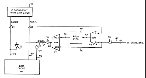
Figure 2 shows a preferred embodiment of the instruction of the
present invention. The PFLoad instruction returns data from external
memory along 64-bit bus 40. The returned data is the data that was
addressed by the third previous PFLoad instruction in accordance with the
pipelined nature of the N10 processor. Tri-state buffer 60 is used to drive
the external data to the "0" input of MUX 62 and also to the DBS input of
2009~~~
MUX 67. Buffer 60 is coupled to multiplexer 62 and 67 through line 61.
Buffer 60, as well as drivers 69, 74 and 75, comprise ordinary tri-state logic
drivers. Similarly, multiplexers 62 and 67 comprise ordinary logic arcuitry
as used in the preferred embodiment. Control for tri-state drivers 60, 69, 74
and 75, as well as muftiplexer 62 and 67, is provided by bus control logic
within the B-unit. This control logic has been synthesized by a computer
from a high-level, functional language description of the bus control unit. A
flow chart of the control operations provided by the B-unit is discussed
later.
The implementation of the PFLoad instruction also includes a
PFLoad first-in-first-out (FIFO) memory 65 coupled from the output of
multiplexer 62 on line 63. FIFO 65 produces an output along 66 which is
coupled to the PFLoad Input of MUX 67.
In the currently preferred embodiment, FIFO 65 is 64-bits long and,
3 words deep. PFLoad FIFO 65 contains the 64-bit data referenced by the
three previous PFLoad instructions. When the processor is initialized, or
following a reset, the contents of the FIFO are undefined. Consequently,
unuseable data or garbage is returned for the first three PFl_oad instructions
(programmers must ignore the data returned for the first three PFLoad
instructions issued).
Multiplexer 67 has one input for receiving data output from the top of
FIFO 65 and another input for receiving data directly from external memory.
External data is directly delivered to MUX 67 via line 61. FIFO 65 is
connected to MUX 67 by line 66. The output of MUX 67 appears on line 68 -
which is coupled to tri-state buffer 69. Tri-state bus buffer 69, in turn, is
coupled to a 64-bit internal bus called a BIBUS, which is shown in Figure 2
as line 29. As its name indicates, this tius is bi-directional, delivering
data
to the floating-point unit as well as returning data from the cache to MUX 62.
BIBUS 29 is coupled to DABUS 76, also 64-bits in length, through buffer 75.
DABUS 76 connects floating-point input data latch 78 to data cache 70. As
previously mentioned, BIBUS 29 is bi-directional to allow the return of data
already residing in data cache 70 to MUX 62 in the event of a cache hit.
11
"' 2009744
Data in the cache is coupled to the BIBUS along line 79 through buffer 74.
When the N 10 processor needs to access data, that data may either
be found in an external memory system or within the internal data cache.
When the data is external to the N10 processor, the PFLoad instruction acts
to load data from external memory, using external bus 40, through
muftiplexer 62 into PFLoad FIFO 65. After three successive PFLoad
instructions have been issued (corresponding to successive FIFO stages),
the initial data is produced on line 66; thereafter delivered onto BIBUS 29.
After the FIFO is full, each normal PFLoad cycle transfers the data from the
top of the FIFO to BIBUS 29, and then to floating-point input data latch 78
via DABUS 76. Thus, each normal PFLoad cycle initiates a corresponding
read cycle within the processor.
As new data arrives from the external data bus it is normally directed
to the bottom of FIFO 65. However, if the addressed data already resides in
the data cache, a PFLoad hit (synonymous with a cache hit) occurs and an
exception is generated. When a PFLoad hit occurs, the bus control logic of
the B-unit will wait until ail outstanding bus cycles are complete. Next, it
transfers the requested data from data cache 70 to the bottom of the FIFO 65
along the data path provided by line 79, buffer 74, BIBUS 29 (coupled to the
"1" input of MUX 62) and line 63.
The controller must wait for all outstanding bus cycles to be complete
before transferring the PFLoad hit data from data cache 70 to the bottom of
FIFO 65 for two reasons. First, there may be a PFLoad cycle outstanding. _
Any attempt to write the PFLoad hit data into the FIFO before ail outstanding
PFLoad cycles are completed will cause the data in the FIFO to ba out of
order. Secondly, BIBUS 29 may already be occupied with c~ta that is being
transferred from a third previous PFLoad instruction to the floating-point
unit.
Bus contention would result if the PFLoad hit data from the cache is
transferred immediately across the BIBUS. To prevent bus contention from
occurring, the bus control logic of the B-unit shuts off buffer 74 for one
extra
clock before putting data back into FIFO 65. After the B-unit waits for all
12
2009744
outstanding cycles to be completed, PFLoad~ hit data is then placed in the
bottom of the FIFO and PFLoad processing proceeds as normal.
it is possible for the processor to operate at a faster rate than the
external bus or memory. For instance, if the speed of the processor is faster
than the external hardware, the FIFO may be emptied. The FIFO is
required to have a sufficient number of stages to hold the maximum number
of addresses issued by the processor and also be compatible with the
pipelined architecture of the processor. Therefore, it is appreciated that the
presently described PFLoad instruction operates dynamically.
Referring now to Figure 5b, the PFLoad FIFO 65 is implemented in
the currently preferred embodiment with three latches or registers per bit, a
read position counter 87, and a write position counter 86. The read position
counter is coupled to decoder 88 which, in turn, is coupled to 3:1 MUX 95
through lines 94 and 93. These lines are coupled to the select lines of
MUX 95 such that, during PFLoad operation, read counter 87 selects the
register from which the next PFLoad cycle will read data.
Write position counter 86 is coupled to decoder 85 which, in turn, is
coupled to registers A, B, and C on lines 92, 91, and 90, respectively.
Lines 90-92 permit data appearing on line 63 to be latched into the
appropriate register. In operation, write position counter 88 points to the
latch to which the next PFLoad cycle will write the returned data. Both the
read position and write position counters comprise ordinary 0-to-2 wrap
around counters.
The read counter is incremented when a PFLoad instruction is in the
write back stage or pending, the BIBUS is not busy and the PFLoad FIFO is
not empty. if the FIFO is empty, the read counter is incremented although
the data is not actually latched in the FIFO but is directly driven to th~
floating-point input data latch. The write counter is incremented when the
current external bus cycle is a PFLoad or when PFLoad data is being
written from the data cache into the bottom of the FIFO for a PFLoad hit. The
two bits of the write position counter are used to generate the FIFO write
13
2009744
signals which latch the data into the FIFO.
An alternative embodiment of FIFO 65 is shown in Figure 5a. Figure
5a shows a FIFO in which the data passes serially from latch t, to latch 2,
and finally to latch 3 before being output on line 66. Although the FIFO of
Figure 5a adequately preserves the pipeline nature of the PFLoad
instructions, it does not have the flexibility of the FIFO shown in F'~gure
5b.
For example, in the FIFO of Figure 5b, data could be written into latch 87 in
one clock cycle and read out in the following cycle without having to pass
through the other registers. Thus, certain data may be made available
earlier if necessary.
As previously stated, the N10 processor can issue up to three
outstanding bus cycles. If the processor is issuing bus cycles at a rate
faster than that of the external memory, the PFLoad FIFO can be emptied.
This implies that the three outstanding cycles are PFLoad cycles. If a fourth
PFLoad cycle is in the write back stage and there is no data available to
load into data latch 78, the bus controller unit issues a freeze. When a
PFLoad cycle is requested but the FIFO is empty, the core must be frozen
until the PFLoad data is available on the DABUS. (A PFLoad is pending
when the data from the FIFO cannot be transferred to data latch 78 due to
the PFLoad FIFO being empty, BIBUS is busy, or a translation-look-s~side
buffer miss.)
It should be noted that when the data cache is doing a normal read,
the data cache unit 70 drives both DABUS 76 and DBBUS 80, so that it
becomes impossible to supply external data to the latch in the same clock
cycle. However, in using a PFLoad instruction, data cache 70 is controlled
by the B-unit logic such that the cache's internal drivers (which are
connected to DABUS 76) are turned oH. By turning off the cache drivers to
DABUS 76, external data can be supplied to data latch 78 without creating
a bus contention situation.
Once PFLoad data becomes available on DABUS 76, the freeze is
lifted. External data is then driven by buffer 75 onto the DABUS from
14
2009744
BIBUS 29. The data supplied along the BIBUS may originate either from
FIFO 65 or directly along line 61 from the external memory system. MUX 67
selects line 61 as the source of the data only when FIFO 65 is empty.
Whether the FIFO 65 is empty depends on the speed of the external
memory, how often the programmer issues PFLoad instnrctions, etc. If the
PFLoad sequence is interrupted, then the data will continue to be slivered
from external memory so long as there are outstanding PFLoad commands
issued on external bus 40. The external data referenced by the previous
PFLoad instructions then accumulates in FIFO 65 until the programmer
once again starts issuing PFLoads.
If the programmer issues successive PFLoad commands s~h that
the data FIFO 65 is emptied before any outstanding PFLoad cycles have
been completed, new data arriving on external data bus 40 will be coupled
along line 61 through MUX 67 to be supplied directly to BIBUS 29. Next, the
data supplied on BIBUS 29 is sent by buffer 75 onto DABUS 76 to
eventually end up stored in floating-point input data latch 78. The data
input latch is actually part of the floating-point unit of the N10 processor.
(The DBBUS is only used when processing 128-bit loads. Since the
PFLoad instruction only operates on 64-bit or 32-bit loads the DBBUS is not
directly related to the PFLoad instruction of the present invention.)
When a data cache hit occurs, i.e., the data requested actually
resides within the data cache and not external memory, then the following
events take place. First, the present word of data has to be returned either -
from PFLoad FIFO 65 or from the external data bus 40. To acoamp~sh this
buffer 75 is shut off by the control logic of the bus control unit and the
data is
returned along the BIBUS path which terminates at the "1" input of
muftiplexer 62. Muttipiexer 62, which is also controlled by the Bus control
unit, then returns the data to the bottom of FIFO 65 along line &3.
In the case where a number of outstanding PFLoads have been
issued - none of which have yet returned data from external memory -- and
a cache hit occurs, a different scenario is presented. In this situation there
Zoo9~44
is nothing that the processor can immediately do with the word of data
presently residing in the data cache. The bus control unit must first wait for
all previously issued PFLoad instructions to return data from external
memory. The first word of data returned is transferred, either from FIFO 65
or directly from the external bus, into data input latch 78 while the
remaining
two words are written to FIFO 65. Finally, the word of data stored in data
cache 70 is transferred to FIFO 65 as the last word in the FIFO. Thus, there
is a substantial time penalty in the case of a cache hit since the programmer
must wait for all outstanding PFLoad cycles to be completed before
transferring the data from the cache to the FIFO. ft should be obvious from
the foregoing discussion that the PFLoad instruction is optimized for a
cache miss rather than a cache hit.
With reference to Figure 4, an alternative embodiment of the present
invention is shown. The circuit of Figure 4 is identical to Figure 2, except
that line 79, buffer 74 and the return BIBUS path to the '1" input of MUX 62
have been eliminated. In their place, bus 81 has been included. Bus 81 is
coupled from the internal buffer 82 of cache 70 directly to the "1' input of
multiplexer 62. The primary benefit realized by this alternative embodiment
is that the user does not have to wait for butter 69 to turn off before
writing
data into FIFO 65. Because there is a dedicated bus 81 included to
accomodate a cache hit, the programmer also does not have to wait for alt
of the external data from outstanding PFLoad instructions to be returned
before proceeding. Nor is there an additional clock penalty since the data
is supplied directly from data cache 70 to FIFO 65 when a cache hit occurs.
On the other hand, the preferred embodiment of Figure 2 enjoys the
advantage of a reduced silicon area since only a single bus is required;
whereas, in the alternate embodiment of Figure 4, additional bus 81 is
needed.
Figure 6 shows a flow chart depicting the control operations provided
by the bus control logic associated with the PFLoad instruction of the
present invention. This flow chart summarizas the foregoing description of
16
"''~' 2009744
the bus control logic exerted during the execution of the PFLoad instruction.
Referring to Figure 6, the PFLoad chart begins with state 100 representing a
PFLoad requost. Once a request has been issued the bus control logic and
the B-unit must determine whether FIFO 65 is empty or BIBUS 29 is busy.
This is shown by decision element 101. If either of those two conditions is
true, the bus controller will wait until the condition changes. If there is
data
present in the FIFO and the BIBUS is not busy, then the controller passes to
state 102 in which data residing in the FIFO is transferred to the
floating-point data latch 78. In decision state 103 the bus controller checks
to see whether or not a PFLoad hit, or alternatively phrased a data cache
hit, has occured. If the data resides in external memory and not in data
cache 70 then the bus controller will issue a PFLoad bus cycle as shown
by state 104. Processing proceeds as normal until the end of the instruction
is reached.
Alternatively, it may happen that a PFLoad hit does occur in which
the bus controller logic must query whether there are any outstanding
PFLoad cycles or whether or not the BIBUS is busy. This is shown in
Figure 6 by decisional point 105. If there are outstanding cycles, or the
BIBUS is busy, the bus controller logic must wait until all outstanding bus
cycles are complete and the BIBUS is available for transfer of data. When
this occurs data is then transferred from the data cache to the bottom of the
FIFO as shown by state 106. The transfer may occur as described in
conjunction with Figure 2 wherein the data passes along line 79 through -
buffer 74 to be returned by the BIBUS to the one input of MUX 62. In the
alternative embodiment, data from the data cache 70 passes directly along
line 81 to the "1" input of MUX 62. Once again, operation proceeds as
normal until the end of the instruction is reached.
In order to more fully appreciate the operation and advantages of the
present invention, reference is now made to the sample operation given in
Figure 3. The sample operation shown by the equation of Figure 3 is:
k V~ + V2 --> V2
17
2009~4~
where k is a certain predetermined constant, V~ is one of 10~ different,
1000 element, vectors stored in external memory and V2 is a vector stored
internally in data cache unit 70. For this particular calculation, the
processor must reuse erector V2 a thousand times (once for each of the
individual elements of each V~) while the individual elements of V~ ars
used only once. Utilizing the PFLoad instruction of the present invention,
the processor loads the individual elements of vector V~ into the
floating-point register without writing over any V2 data resident in the data
cache.
Figure 3 shows a first PFLoad instruction, pfki~, being issued to the
address of V» in order to load the first element of the first V~ vector into
floating-point storage location f2. The pfldt command takes two clock
cycles to initiate. Without waiting for the data to return from external
memory, a second PFLoad instruction, pfld2, is issued to address vector
element V~2 and directs it to floating-point storage location fa. Additional
PFLoad commands are initiated for vector elements V~3, V», V15, etc. A
new PFLoad can be requested every two clocks since the external bus
permits a new address to be issued every two clocks.
When the fourth PFLoad command is issued, i.e., pfld;, exiemal
memory begins to return the data from the first PFLoad instruction. This
returned data actually corresponds to the third previous PFLoad instruction
so that the destination register specified in the fourth PFLoad is the f2
register. The arrival of the data from the third previous PFLoad command is -
shown by the dashed lines and arrows directed diagonally from the
floating-point storage location to the address of the PFLoad command. The
programmer may continue to specify PFLoads every two clocks in
accordance with the full bandwidth capability of the external bus. In
practice, there is a total of six clocks of latency from the time that the
programmer specifies the data address to the time that data returns. So the
memory system has a total of 6 clocks to provide the data even though a
new bus cycle is starting every other clock. This means that a 3X speed
18
'~' 2009744
increase in the rate in which cycles can be processed is realized. Without
the pipeline approach, the programmer would be restricted to issuing a new
cycle every six clocks instead of every other clock.
It should be understood, of course, that the foregoing discussion
assumes that each PFLoad instnrction corresponds to a data cache miss. ff
this was a normal floating-point load in a prior art processor, as soon as the
programmer tried to perform a second PFLoad the bus control unit would
respond that there is an outstanding access and then freeze up for the entire
six clocks -- waiting for outstanding bus loads to return. Therefore, in a
prior
art processor the programmer can only issue a new address every six
clocks instead of every other clock. Thus, the pipeline approach
associated with the PFLoad instruction of the present invention allows the
user to issue addresses at a faster rate, despite the tact that the data is
not
resident in the onboard cache. It therefore allows efficient processing and
accessing of very large data stnrctures.
The present invention allows the vector V2 to be stored onboard
while the V1 element is kept in external memory so that the user may
reference V1 elements using a PFLoad instruction and reference V2 with a
normal load instruction. In a typical prior art microprocessor without a
PFLoad instnrction, each time the user references Vt , data elements would
be brought into the cache thereby forcing out the elements of vector V2.
This would create additional delay the next time the V2 element would have
to be loaded.
Whereas many alternations and modifications of the present
invention will no doubt become apparent to a person of ordinary skill in the
art after having read the foregoing description, it is to be understood that
the
particular embodiment shown and described byway of illustration is in no
way intended to be considered limiting. For example, although this
disclosure has shown a particular way of implementing the ~petine
floating-point load instruction, other implementations are possible.
Therefore, reference to the details of the preferred embodiment are not
19
2009744
intended to limit the scope of the claims which are themselves recite only
those features regarded as essential to the invention.
Thus, a pipelined floating-point load instruction for accessing
infrequently referenced data from external memory has been described.