Note: Descriptions are shown in the official language in which they were submitted.
C~ ~
Z~ )5
, . , . . . . . . ......... . . . . . , . _ . .. _,
PHA.21486 1 14-12-1989
Two-lead igniter for ~lD lamps.
This invention relates to starting devices
for high intensity discharge (HID) lamps and, more
particularly, to a universal two-lead igniter useful
in the ignition of metal halide and other HID lamps.
Various forms of presently available HID lamps,
especially metal halide lamps, require voltage spikes
on the order of several thousand volts in order to
produce reliable ignition of the lamp. In order to
generate these very high voltages economically, various
electronic devices and circuits have been designed and
are employed commercially at the present time. The energy
- transformation technique used in these conventional
lamp ignition devices generally utilize the coil and/or
capacitor of the lamp ballast apparatus in order to step
up the available 6û Hz AC line voltage to the KV range.
Fig. 1 of the drawing illustrates a common
form of lamp igniter circuit in general use today which
will be discussed in greater detail below. Briefly,
the capacitor (11) gradually charges up to the voltage
20 breakdown level of the Sidac (13), whereupon the
capacitor discharges rapidly through the Sidac and a
small part of the transformer secondary winding. This
voltage is stepped up via the transformer to develop
a large voltage, i.e. several KV, across the entire
secondary winding and hence across the lamp to produce
lamp ignition. A disadvantage of this starter-igniter
device is that the high-voltage collapses fairly rapidly
which makes the lamp ignition less than entirely reliable.
This problem can be minimized by modifying the ballast-
30 igniter circuit in the manner described in U.S. PatentNo. 4,695,771.
- 20~98~)5
PHA.21486 2 14-12-1989
U.S. Pat. No. 4,339,695 describes 8 high
pressure sodium (HPS) lamp ballast circuit that utilizes
a conventional igniter to start a high pressure discharge
lamp. This circuit requires a pulse auto-transformer
with a tap point in order to generate a high voltage
ignition pulse in the order of 25ûû to 400û volts.
Figs. ~ and 2 of this patent show an igniter consisting
of the pulse auto-transformer, a Sidac solid state
switch, a capacitor and a resistor which is used to
charge the capacitor. A clamping circuit is coupled to
the igniter and consists of eight components (Fig. 1)
or six components (Fig. 2). The clamping circuit is
required in order to limit the VA rating of the ballast
which operates the HPS lamp during starting, hot restart,
and lamp out conditions.
The pulse auto-transformer as shown in USP
4,339,695 is connected in series with a lamp across
the secondary winding of the ballast. The large number
of components makes the whole system uneconomical and
by adding power losses thereto it also makes the system
relatively inefficient. In the case where the lamp is
not connected, or during the initial starting phase,
the conventional igniter produces a single voltage pulse
near the peak of the open circuit waveform of the
secondary winding output voltage, but not at the lower
end thereof (Fig. 3 of USP 4 339 695).
Another starting circuit for discharge lamps
is shown in U.S. Pat. No. 3,758,818. This starting
circuit uses two closed circuits that share a common
capacitor. The first closed circuit includes a power
source and an inductive stabilizer in combination with
the capacitor. The second closed circuit includes an
inductor and a bidirectional diode thyristor in combination
with the capacitor. A second bidirectional diode thyristor
having a lower break-over voltage than the first one is
provided and constitutes, along with the second closed
circuit, a starting circuit for the lamp. In the
- second closed circuit, the capacitor is charged via ~he
20~398~)5
PHA.21486 3 14-12-1989
second bidirectional diode thyristor to the instantaneous
value of the power source and is discharged by the first
bidirectional diode thyristor through the inductor which
produces a high voltage pulse which is applied to the
lamp to start it. The output voltage waveform shows a
high frequency oscillation only at the top portion of
the open circuit voltage waveform. Disadvantages of this
circuit are the requirement for two switching devices
and the large number of circuit components which makes
it expensive and less efficient.
A further discharge lamp starter device which
uses a backswing voltage booster is described in U.S.
Pat. No. 3,866,088. This starter circuit consists of
the backswing voltage booster which includes a capacitor
connected across the lamp for oscillation, a series
circuit of a saturable non-linear inductor and a
- bidirectional diode thyristor, and a current limiting
capacitor connected across the non-linear inductor.
The output of the booster is in the form of an oscillating
voltage which is produced by the switching action of the
bidirectional diode thyristor together with the operation
of the capacitor discharging through the non-linear
reactor that produces the high voltage pulses that appear
across the common capacitor producing oscillation of the
output voltage from the power source. The starter
device according to USP 3,866,088 requires the presence
of a non-linear inductor. The cost of such a starter
device is relatively high and the circuit efficiency
is not optimum.
Furthermore, in the known circuit, if the
discharge lamp is inadvertently removed, the continuous
oscillation and the magnitude of the boosted voltage
will cause damage or destruction of the circuit components
if the non-linear inductor is not biased properly.
The output to the discharge lamp can be controlled by
a bias means for negatively or positively exciting the
magnetic field of the core of the saturable non-linear
8~5
PHA,21486 4 14-12-1989
reactor. Therefore, an added bias coil winding has to be
provided for fail safe protection in order to limit the
oscillating period and the magnitude of the boosted
voltage.
It is therefore an object of this invention
to provide an improved starting device for HID type
lamps that is not subject to the disadvantage and
limitations of the prior art lamp starting devices.
Another object of the invention is to provide
a two-terminal igniter-starter for starting HID type
discharge lamps, for example, dual-ended metal halide
lamps, that is more economical and efficient than
currently available starter devices.
A further object of the invention is to provide
a new and improved igniter-starter device that does not
require a tapped ballast inductor or transformer or a
separate pulse transformer in order to generate high
voltage ignition pulses for starting HID lamps or the
like.
Another object of the invention is to provide
a circuit for operating a HID type lamp including an
improved igniter-starter circuit that is responsive to
a relatively low voltage, low frequency (e.g. 60 Hz)
supply voltage to produce a high frequency, high voltage
open circuit voltage waveform that provides reliable
ignition of the lamp without a step-up transformer.
In accordance with the invention, the foregoing
and other objects and advantages of the invention are
achieved by the provision of a two-terminal igniter-
starter circuit that is adapted for connection inparallel with a high intensity discharge lamp and which
comprises a first circuit including a resistor and
capacitor connected together to form a parallel RC
network which is in turn connected in series circuit
with a second network that includes one or more passive
components such that the first and second networks
provide a resonant effect that produces a high frequency,
high voltage open circuit ignition voltage waveform
20G98~5
PHA,21486 5 14-12-1989
when the starter-igniter circuit is energized from a
low frequency (for example, 60 Hz.) approximately
sinusoidal AC voltage supply source. A voltage-responsive
bidirectional switching element is included in one of
said first and second networks.
In a first preferred embodiment of the
invention, the first network of the igniter-starter
circuit comprises a first resistor and first capacitor
connected in parallel and the second network comprises
the voltage-response bidirectional switching element
(e.g. a Sidac) connected in series with the parallel
combination of a second resistor and a second capacitor.
The two parallel RC networks together form an oscillatory
circuit each time the series connected switching element
breaks into conduction thereby to generate a high
frequency, high voltage oscillatory voltage that is
- superimposed on the input sinusoidal AC supply voltage.
The resultant high frequency AC waveform is generated
over the entire period of the low frequency AC supply
voltage thereby providing a high amount of electric
energy that produces improved and more reliable ignition
of a HID lamp connected in parallel with the igniter-
starter circuit.
In a second preferred embodiment of the
invention, the voltage-responsive bidirectional switching
element is connected in the first RC parallel network
and the second network includes an inductor and a second
capacitor connected in series circuit with each other
and with the first RC parallel network. A similar open
circuit distorted high frequency voltage waveform will
be generated for improved ignition of a discharge
lamp connected in parallel with the igniter-starter
device.
A third embodiment of the invention utilizes
a first parallel RC network in series with a second
network comprising a series circuit that includes the
voltage responsive bidirectional switching element,
Z(~G~8 [1~;
PHA.21486 6 14-12-1989
an inductor and a second capacitor. In this embodiment,
the ratio of the capacitance C1 of the first capacitor
to the capacitance C2 of the second capacitor is
preferably greater than in the first embodiment described
above. This will increase the distorted peaky open
circuit voltage of the ballast, which provides this
igniter-starter circuit with a better restrike capability.
An advantage of the invention is that the
igniter-starter requires only two leads to connect it
lo to the discharge lamp. Furthermore, it can be connected
in parallel with the lamp and thus can be powered from
the output of the ballast, i.e. from an AC voltage source.
It does not require a tapped transformer, nor a pulse
transformer, which makes it inexpensive and further
simplifies the wiring connections.
A further advantage of the invention is that
the igniter-starter circuit automatically switches
itself out of the overall lamp operating circuit after
the lamp ignites because the lamp operating voltage is
lower than the threshold voltage of the voltage-responsive
bidirectional switching element. This reduces the overall
power losses in the circuit, resulting in a more efficient
apparatus. Electromagnetic interference is also reduced.
The starter device described in USP 3,866,088
generates a somewhat similar distorted oscillating
oùtput voltage to that generated in the present invention,
but requires a more complicated and expensive circuit
to accGmplish the lamp ignition function. The known
starter absolutely requires the presence of a relatively
costly non-linear inductor, whereas the present invention
produces the distorted oscillating output voltage waveform
by the simple combination of a resistor (R) and capacitor
(C) connected in parallel, a bidirectional solid state
switch and a second simple passive network connected
in series circuit with the parallel RC combination.
The pulse amplitude and frequency of operation of this
invention is not as high as that of the known circuit
thereby making the present circuit more convenient for
20~ )5
PHA.21486 7 14-12-1989
the ignîtion of metal halide lamps.
Furthermore, in the apparatus known from
USP 3,866,088, if the lamp is removed or becomes
inoperative with the power applied, the apparatus
continues to oscillate and the magnitude of the boosted
voltage is such as to cause destruction of the circuit
components unless a protective bias is provided for the
saturable non-linear reactor. In particular, in the USP
3,866,088 an extra bias coil is provided for fail safe
protection by limiting the oscillating period and the
magnitude of the boosted voltage. In this invention
over-voltage protection is automatically provided by
the symmetrical switch (Sidac) because it acts like a
fuse if the lamp is removed or becomes inoperative.
ls Besides, the resistors are connected across the capacitors
thereby limiting their charging and discharging charac-
teristics.
In contrast to the circuit known from USP
4,339,695, the first embodiment of the invention, al~hough
it also uses a Sidac semiconductor switching device,
uses a simpler and less expensive circuit to develop
a peaky ringing voltage across the two capacitors.
This is accomplished by simply switching the Sidac
on and off. Fig. 3 of USP 4,339,695 shows a secondary
voltags waveform with a single voltage peak or spike
with the lamp out or prior to lamp ignition. In comparison,
the oscillating high frequency pulsing voltage generated
by the series connection of first and second parallel
RC circuits, as the semiconductor Sidac switches on and
off, distorts the output voltage of a conventional
ballast resulting in an output voltage waveform with
multiple voltage peaks that is very different from the
voltage generated in apparatus shown in USP 4,339,695.
The patent, 3,758,818, requires first and
second bidirectional diode thyristors and an indu~tor
and produces an output voltage waveform with oscillations
that occur only near the peak of the low frequency
Z~ ~ 9 8~ S
PHA.21486 a 14-12-1989
open circuit voltage waveform. The invention herein uses
a simple circuit that does not require dual switching
devices to charge and discharge the power supply voltage
into an inductor. In the first preferred embodimen$ of
the invention, two closed circuits are provided, each
consisting of merely capacitors and resistors. The
capacitors are charged and discharged from the power
source at the secondary circuit of the lamp ballast
by means of a single bidirectional Sidac device
switching on and off. The switching of this Sidac
generates a distorted high frequency oscillating voltage
which occurs over the entire time period of the AC power
supply, i.e. it is not confined only to the top portion
of the low frequency supply voltage waveform.
The simplicity of the invention makes it more economical
and efficient than the apparatus shown in USP 3,758,818.
The provision of the high frequency voltage waveform
over the entire period of the AC supply voltage produces
more energy for the discharge lamp and thereby improves
the ignition characteristic.
The organization and method of operation of
the invention, its novel features together with further
objects and advantages thereof, may best be understood
by reference to the following detailed description
taken in conjunction with the accompanying drawings,
in which:
Fig. 1 shows a prior art igniter circuit for
a discharge lamp,
Fig. 2 is a schematic circuit diagram of a
first embodiment of tne invention,
Fig. 3 is a scematic circuit diagram of a
second embodiment of the invention, and
Fig. 4 is a schematic circuit diagram of a
third embodiment of the invention.
In order to better illustrate the various
features and advantages of the invention, a brief
description will first be given of one exemplary
- 20~
PHA.21486 9 14-12-1989
prior art starter-igniter circuit (Fig. 1). The lamp
igniter circuit shown in Fig. 1 consists of a transformer
1 for coupling a source 2 of AC voltage (50/60 Hz~
to a HID lamp 3. The AC voltage is coupled to the primary
winding of the transformer upon closure of a line
switch 4. A three-terminal or three-lead igniter device
5 is coupled to the secondary winding of the transformer
and to the discharge lamp 3.
The igniter 5 has terminals 6, 7 and 8.
Terminal 6 is connected to a line 9 coupling one end
of the transformer secondary winding to one electrode
of the lamp 3. Terminal 7 connects the igniter to a
line 10 that couples the other end of the transformer
secondary winding to the other electrode of lamp 3,
while terminal 8 of the igniter is connected to a tap
on the secondary winding of the transformer. The trans-
former may be designed as a leakage transformer to
provide the customary current limiting ballast function
in the operating condition of the diacharge lamp.
The tapped secondary winding provides the additional
function of a step-up transformer to generate the
required high voltage ignition pulse for the HID lamp 3.
The igniter 5 also includes a capacitor 11
and a resistor 12 connected ins eries circuit between
the terminals 6 and 7. A Sidac 13 or similar voltage-
breakdown element is coupled between terminal 8 of the
igniter and a junction point between capacitor 11 and
resistor 12.
When the switch 4 is closed and power is first
applied to the ballast transformer, the capacitor is
charged through resistor 12 as a result of the voltage
induced in the secondary winding. The HID lamp 3 is
not yet on since it requires several thousand volts
to strike the arc, whereas the voltage induced in the
transformer secondary initially is only of the order
of two or three hundred volts, which is produced by a
conventional ballast transformer.
Z(~ 805
PHA.21486 10 14-12-1989
The switching device (Sidac) 13 is ~open"
until the capacitor charges up to the voltage-threshold
(breakdown) level of the Sidac, at which time the Sidac
switches to the "on" state. This allows the capacitor
to rapidly discharge across the relatively few winding
turns between the tap point and the top end of the
transformer secondary winding. This produces, via the
step-up transformer action, a large voltage in the
order of several kilovolts across the entire transformer
secondary winding. This high voltage will appear across
the lamp and cause it to ignite.
An undesirable effect of this circuit is that
it causes a marked collapse in the waveshape of the low
frequency (60 Hz.) transformer voltage because the
discharged capacitor presents a significant load to the
transformer thereby causing a substantial dip in the
voltage waveform.
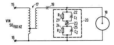
Fig. 2 is a circuit diagram of a first embodiment
of the starter-igniter apparatus in accordance with the
invention. The customary AC supply voltage of 277 volts
at 50/60 Hz is applied to input terminals 15-16.
A constant wattage autotransformer 17 supplies an AC
voltage of the order of 270 RMS volts to a double-ended
metal halide discharge lamp 18 via a series connected
capacitor 19. The autotransformer and capacitor provide
the customary ballast function for limiting lamp current
when the lamp is in its normal operating condition.
A two-terminal starter-igniter device 20
is connected in parallel with the discharge lamp.
In accordance with the invention, the igniter device
includes a first parallel RC network composed of a
resistor 21 of resistance R1 and a capacitor 22 of
capacitance C1. A second network, consisting of a
bilateral semiconductor switch 23, for example, a Sidac,
in series with a second parallel RC network including a
resistor 24 of resistance R2 and a capacitor 25 of
capacitance C2, is connected in series circuit with the
first RC network between the two terminals of the starter
2~ 8~5
PHA.21486 11 14-12-1989
circuit 2û. The series circuit 21-25 is thus in parallel
with the discharge lamp 18.
The usual peaky type open circuit voltage
waveform provided by the constant wattage auto transformer
ballast is further distorted by a high frequency voltage
generated by the two-lead igniter 20. Ringing voltages
are generated by the parallel RC combination of resistor
21 and capacitor 22 and by the further parallel RC
network consisting of resistor 24 and capacitor 25.
Switching of the ringing voltage is accomplished by the
bilateral semiconductor switch 23. The total voltage
generated across the terminals of the igniter 20 is the
vector sum of the oscillatory voltages developed across
the first parallel RC network (21, 22), the second
parallel RC network (24, 25) and the breakover voltage
of the Sidac 23.
An examplary set of values for hhe circuit
components of the apparatus of Fig. 2 is R1=3.3 Mohms,
C1=0.47 ~ Fd, R2=1.5 ohms, and C2=0.33 ~ Fd.
The Sidac 23 may have a breakover voltage in the range
of 235-260 volts where the igniter is used in combination
with a constant wattage autotransformer for operating
175 W and 250 W metal halide double-ended discharge lamps.
The values of the starter circuit components will differ
for various types of ballasts and lamps. Nevertheless,
the mode of operation of the circuit, as described above,
remains essentially the same.
The igniter 20 of Fig. 2 develops a peaky
ringing voltage across the two capacitors which is
switched on and off by the Sidac. The series-parallel
combination of only five components, none of which is
an inductor or pulse transformer, is connected across
the lamp and secondary circuit of the ballast to generate
a high pulse oscillating voltage which improves and
makes more reliable the ignition of a metal halide lamp.
The oscillating high frequency pulsatory voltages
generated by the two parallel RC networks as the Sidac
is switched on and off distorts the output voltage of the
98~)5
PHA.21486 12 14-12-1989
secondary circuit of the conventional ballast in a manner
that produces an output voltage waveform for igniting
the lamp that is very different from, and more effective
than, that produced by prior art starter circuits.
Fi8. 3 illustrates a second embodiment of the
starter-igniter apparatus in accordance with the invention.
Similar circuit elements will be designated by the same
reference numerals as in Fig. 2. This circuit is similar
to Fig. 2 except that the igniter now is used in
combination with an autotransformer lag ballast (not
shown in detail for the sake of simplicity). Input
terminals 15-16 are again connected to an AC supply
voltage of, for example, 240 volts at 50-60 Hz.
The igniter 20 omits the resistor 24 of Fig. 2 but now
includes an inductor 26 connected in series with the
capacitor 25. The Sidac 23, the inductor 26 and the
' capacitor 25 are connected in a series circuit. This
series circuit is connected in series with the parallel
RC network 21, 22 between the two terminals of the
igniter 20, hence in parallel with the metal halide lamp
lB. Of course, the components values are different than
those in the igniter of Fig. 2. For example, the
capacitance C1 of capacitor 22 is increased in order to
increase the distorted peaky open circuit voltage of the
ballàst thereby enabling the starter circuit to prnduce
a better restrike capability.
A third embodiment of the invention is shown
in Fig. 4 where, once again, similar circuit elements
are designated by the same reference numerals as in the
circuits of Figs. 2 and 3. In the starter 20 of Fig. 4,
the resistor 21 now is connected in parallel with the
series combination of capacitor 22 and Sidac 23.
The parallel network 21-23 is serially connected with
an inductor 26 and the capacitor 25 between the two
terminals of the igniter 20, which are in turn connected
to the lamp electrodes so that the igniter circuit is
again in parallel with the discharge lamp. This embodiment
20~38~)5
PHA,21486 13 14-12-1989
generated a distorted high frequency peaky open circuit
voltage ~waveform similar to that generated by the
igniter circuit of Fig. 2.
It will be apparent from the above description
that an improved starter-igniter device for HID lamps
is provided which requires only two leads or terminals
for connection to a lamp-ballast apparatus, and which
eliminates the need for expensive pulse transformers
or the like as was customary heretofore.
Although the invention has been shown and
described in connection with certain preferred embodiments
thereof, it will be apparent that such embodiments are
provided by way of explanation and example only since
numerous variations,changes and substitutions will occur
to those skilled in the art without departing from the
spirit and scope of the invention disclosed.
Accordingly, it is intended that the invention be
li~ited only to the extsnt required by the language
of the appended claims.