Note: Descriptions are shown in the official language in which they were submitted.
2010206
1 62046-220
Pulse-Spaclng Decoding
The present lnvention relates to a clrcult arrangement
for decodlng pulse spaclngs, preferably for fllterlng pulse
sequences wlth a glven spaclng therebetween out of a composlte
slgnal.
In radlo navlgatlon systems, partlcularly ln the alr
navlgatlon system DME ~Dlstance Measurlng Equlpment~, pulse
sequences are generated which must be flltered out of a composlte
slgnal by a ground statlon and/or an alrborne statlon for checklng
or evaluatlon purposes (E. Kramer, "Funksysteme fur Ortung und
Navlgatlon~, Verlag Berllner Unlon GmbH, Stuttgart, 1973, pages
147 to 157).
The ground statlons transmlt at predetermlned tlme
lntervals an ldentlflcatlon whlch conslsts of a traln of pulse
pairs ln a Morse code. After decodlng, the ldentlflcatlon pulses
form a perlodlc pulse sequence of 1350 Hz. The code can thus be
made audlble for the pllot and for the personnel of the ground
statlon.
So far, lt has not been customary to monltor the trans-
mltted ldentlflcatlon for completeness ln the ground statlon.
Only an occaslonal acoustlc check of the audlble Morse code has
been made by the personnel of the ground statlon. The selectlon
of the ldentlflcatlon from the composlte slgnal recelved from the
transmltter has been made by a correlator conslstlng of an lnput
shlft reglster, a reference reglster, and a sultable number of
comparators. Wlth a ~ustlflable amount of clrcultry, the
resolutlon attalnable wlth such an arrangement ls llmlted.
A ~$
2010206
_
~ 62046-220
To measure the slant dlstance between alrcraft and
ground statlon, the alrborne statlon transmlts pulse palrs whlch
are acknowledged by the ground statlon by tlme-shlfted palrs of
reply pulses. The tlme lnterval between the two pulses ls the
channel ldentlflcatlon. The latter must be recognlzed both by the
ground statlon and by the alrborne statlon. So far, a delay llne
has been used for thls purpose whlch provldes a delay equal to the
tlme lnterval between the pulses. The accuracy achlevable wlth
such a delay llne ls not sufflclent, however.
It ls, therefore, the ob~ect of the lnventlon to provlde
a clrcult arrangement whlch permlts accurate checklng of pulse
spaclngs.
Accordlng to a broad aspect of the lnventlon there ls
provlded a clrcult arrangement for decodlng pulse spaclngs between
lncomlng pulse slgnals, partlcularly for navlgatlon systems,
comprlslng: the serles comblnatlon of a pulse shaper and a random-
access memory havlng a plurallty of cells; clock means for gen-
eratlng count clock perlods lndlcatlve of the readlng or wrltlng
of cell contents; address counter reglster means for addresslng
cells of the random-access memory and havlng a count cycle of
count clock perlods; and an AND gate, the lnput and output of the
random-access memory belng respectlvely connected to the two
lnputs of the AND gate, whereln the length of the count cycle of
the address counter reglster means is equal to a spaclng between
two consecutlve lncomlng pulse slgnals wlth a predetermlned
spaclng, and that durlng each count clock perlod, contents of the
addressed cell of the random-access memory are read out and the
2a 201o206 62046-220
current slgnal state recelved from the pulse shaper at the lnput
of the random-access memory ls wrltten lnto the same cell, such
that pulse slgnals wlth the predetermlned spaclng there-between
are decoded and form the output slgnal of the clrcult whlch can be
taken from the output of the AND gate.
Accordlng to another broad aspect of the lnventlon there
ls provlded a clrcult arrangement for fllterlng out consecutlve
palrs of pulses wlth a predetermlned spaclng therebetween from an
lncomlng composlte slgnal, comprlslng: pulse shaplng means for
recelvlng pulses of lncomlng slgnals and outputtlng modlfled pulse
slgnals; a random-access memory havlng a plurallty of cells for
storlng lnputted pulse slgnals, an lnput of the random-access
memory belng connected to the output of the pulse shaplng means;
clock means for generatlng count clock perlods, each clock perlod
generatlng a read and wrlte slgnal; reglster means for addresslng
cells of the random-access memory ln response to a count cycle of
count clock perlods; and an AND gate, the lnput and output of the
random-access memory belng respectlvely connected to the two
lnputs of the AND gate, whereln the count cycle of clock perlods
has a duratlon equal to the predetermlned spaclng of consecutlve
pulses to be flltered, and that durlng each clock perlod, the
content of the addressed cell of the random-access memory ls
outputted ln response to the read slgnal and the slgnal output
from the pulse shaper ls wrltten lnto the same cell ln response to
the wrlte slgnal, such that the AND gate outputs the decoded
pulses wlth the predetermlned spaclng therebetween.
The prlnclpal advantages offered by the lnventlon are
that the use of a random-access read/wrlte memory wlth a
A
~0206
-- 3
great number of cells permits optimum resolution and,
thus, very accurate checking of the pulse spac;ngs, and
that the circuit complexity and space requirement
are comparatively low.
Theinvention will be better understood by reference to
the description of two applications taken in conjunction
with the accompanying drawings, in which:
Fig. 1 is a block diagram of a circuit arrangement
in accordance with the invention;
Fig. 2 shows the timing diagram for a first appli-
cation, and
Fig. 3 shows the timing diagram for a second appli-
cation.
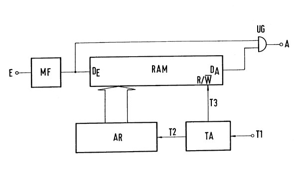
Thepulse-spacing-decoding circuit shown in Fig. 1 con-
sists of the series combination of a monostable multi-
vibrator MF and a random-access memory RAM, an AMD
gate UG whose two inputs are connected to the input
DE and the output DA, respectively, of the random-access
memory RAM, an address counter register AR associated
with the random-access memory RAM, a clock conditioner
TA, and a generator (not shown) providing a basic clock
signal T1. The clock conditioner TA derives from the
basic clock signal T1 count pulses T2 by which the
address count register AR is incremented. The length of
the count cycle ZZ ~Figs. 2 and 3) can be adjusted depending on
J. Gutekunst 3
Z~
the specific appLication. A read/write input R/W of
the random-access memory RAM is fed with read/wr;te
pulses T3 which are produced by the clock conditioner
TA in synchronism with the counting pulses T2. In the
second half of each T3 clock period, a change of state
of the signal at the input R/W causes the signal applied
at the input DE of the random-access memory RAM to be
written into the addressed cell, whose content was pre-
viously read out via the output D~. During the "read"por-
tion of the clock period, the current input signal and the
signal stored in the re-addressed cell during the pre-
ceding count cycle ZZ (Figs. 2 and 3) are applied to the
AND gate UG. When both inputs of the AND gate are at
logic 1, the AND gate is enabled. The change of state at
the output A indicates that two pulses with the pre-
determined spacing were recognized. The monostable multi-
vibrator MF connected ahead of the random-access memory
RAM serves as a pulse shaper. Its dwell time is equal to
the clock period T2.
Fig. 2 shows the identification KB of a ground station
in the DME system and the timing diagram for recognizing
this identification with the circuit of Fig. 1. The
identification KB consists of a 3-letter Morse code
(shown only in part) (Fig. 2a). The pulses of the Morse
code are formed from a plurality of periodic pulse pairs
PP with a repetition rate of 1350 Hz (Fig. 2b). The
identification KB, transmitted at ~0-ms intervals, ;s
contained ;n a composite signal derived from the
J. Gutekunst 3
20~0~
transmitter noise and consisting of randomly d;stributed
pulses. Via the criterion of the pulse pairs PP re-
curring at a rate of 1350 Hz (Fig. 2b), the identification
KB can be filtered out of the composite s;gnal with the
aid of the circuit arrangement of Fig. 1.
Thepulses decoded as described above are applied to the
input E of the circuit of Fig. 1. They are conditioned
in the monostable multivibrator MF, whose dwell time is
equal to the clock period T2, here 13 ~s (Fig. 2d). The
duration of the count cycle ZZ of the address
counter register AR is equal to the
pulse spacing to be recognized. Only pulses whose spacing
is equal to this cycle duration ZZ are recognized as
such. The circuit of Fig. 1 thus acts like an extremely
sharp-cutting filter.
Fig. 2c shows two periodic pulses Px and Pxf1, which are
derived from the pulse pairs PPx and PPxt1 (Fig. 2b)
by decoding. As their repetition rate is 1350 Hz, the
time interval between them is 741/us. To this interval,
the count cycle ZZ with fifty-seven 13-/us clock periods
T2 is adjusted. As mentioned above, each pulse appearing
at the input E is brought to the duration of 13 ~s
(Fig. 2d) by the monostable multivibrator MF. This is
necessary in order to always have the same conditions
during the subsequent processing. As the incoming
pulses and the count pulses T2 are not in synchronism,
the synchronism between the monostable-multivibrator pulses
and the addressing of a memory cell, shown in
J. Gutekunst 3
20~0~
Fig. 2 for the sake of simplicity, will occur rarely. It
is irrelevant, however, whether the count pulses T2
lead or lag the respective monostable-multivibrator pulses,
because the pulses following after a cycle duration ZZ
are sampled under the same conditions and, therefore,
have the same form. It is equally irrelevant in which
of the cells A1 to A57 of the random-access memory RAM
a signal state was stored, because the cycle ZZ remains
the same, so that a pulse occurring after the pre-
determined cycle duration will be up for evaluation at
the moment the corresponding cell is addressed again.
Figs. 2c to 2e illustrate this. The first periodic pulse
Px is changed by the monostable multivibrator MF into
a pulse which is presented to the input DE of the ran-
dom-access memory RAM for 13/us. During th;s time, the
content of the addressed cell, here A1, is read out.
Let us assume that the cell A1 is empty, so that the
AND condition for the AND gate UG is not satisfied. In
the last third of the clock period T2, the current sig-
nal state at the input DE is written into the cell A1
via the change of state of the readlwrite signal T3.
At the beginning of the next count cycle ZZ, the next
periodic pulse Pxt1 appears. At the same time~ the
cell A1 is addressed again. The content of the latter
is now equal to the logic level at the input DE, so
that the AND condition for the AND gate UG is satisfied.
During the subsequent "write" port;on of the clock
period, the current signal state is again written into
the cell A1. Thus it is ensured that pulses with only
slightly different spacings are suppressed. De-
pending on the capacity of the random-access memory
J. Gutekunst 3
2010206
RAM, the resolution can be var;ed within wide Lim;ts
if necessary.
Fig. 3 shows the timing diagram if the circuit arrange-
ment of Fig. 1 is used to decode the spacing PA between
the single pulses P1 and P2 of a pulse pair DP of the
kind mentioned at the beginning.
The received pulse pair DP is digitized by a 50% Schmitt
trigger ST and then applied to the input E of the c;r-
cuit of Fig. 1. As in the previous example, the shape of
the pulse pair is changed by the monostable mult;vibrator
MF. At a clock rate of 5 MHz, for example, the c~ock
period and, thus, the dwell time of the monostable
multivibrator MF are 200 ns. Here, too, the count-cycle
duration ZZ of the address counter register AR ;s equal
to the pulse spacing PA to be recognized. The cyclic
read/write operation of the successively addressed
memory cells A1 to An is performed essentially as
described above. Here, too, a signal appears at the out-
put A of the circuit arrangement of F;g. 1 if the ad-
dressed memory cell and the signal at the input DE of
the random-access memory RAM are at logic 1 at an
interval equal to the count-cycle duration ZZ. The
extremely high resolution of 200 ns ensures that pulse
pairs with a spacing differing by more than 200 ns
are reliably excluded.
J. Gutekunst 3