Note: Descriptions are shown in the official language in which they were submitted.
2010393
COMMUNICATION SWITCHING SYSTEM
The present invention relates to a communica-tion
! switching system including a switching network with at
least one switching element having a pluralitY of input
links and at least one output link, and processing means
for calculating the total bandwidth used by virtual paths
on said output link from individual bandwidth values
contained in path setuP cells used for setting up said
virtual paths.
Such a communication switching sYstem is already
described in the PCT application No PCT~EP88/00482 (P.
BARRI et al 4-1). In this known switching sYstem the total
bandwidth used by the virtual paths on an outPut link is
obtained by calculating the sum of the individual bandwidth
values contained in the path setup cells for these paths.
A new virtual Path is allowed to be multiplexed on the
output link only when the thus calculated total bandwidth
is smaller than the maximum allowable bandwidth.
The thus calculated total bandwidth maY be erroneous
due to a fault, for instance because an individual
bandwidth value is erroneous, or due to a calculation
error, etc. Such a fault may give rise to a traffic
overload on the output link or to an undue restriction of
the traffic load on this link since the decision to allow
or inhibit the multiplexing of a new virtual Path on an
output link is based on the thus calculated total
bandwidth.
2010393
An ob~ect of the present lnvention is to provlde a
communication switching system of the above type, but wherein
the effect of previous, especially temporary errors, on the
calculated total bandwidth is reduced.
According to the invention this ob~ect ls achleved
due to the fact that sald processlng means re-calculate sald
total bandwldth at least from sald lndlvidual bandwidth values
contalned ln malntenance cells transmltted on sald virtual
paths and ad~ust said calculated total bandwidth to correspond
to sald re-calculated total bandwldth.
By thus recalculatlng the total bandwldth the effect
of temporary errors whlch possibly occurred durlng a prevlous
calculatlon ls reduced lf not ellmlnated.
Another characteristlc feature of the present
communlcation switching system ls that the transmlsslon of
sald malntenance cells is lnterleaved wlth that of sald path
setup cells and that sald processlng means store sald
calculated total bandwldth ln a flrst memory and at the start
of a recalculatlon operatlon copy sald calculated total
bandwldth from sald flrst memory lnto a second memory and
reset the contents of a third memory, the total bandwidth
stored in said second memory and sald lndlvldual bandwldth
values belng then used to re-calculate sald total bandwldth ln
a cumulatlve way and the successive partlal results thus
obtalned belng stored ln sald thlrd memory.
Stlll another characterlstlc feature of the present
communlcatlon swltchlng system ls that the transmlsslon of
sald maintenance cells is also lnterleaved wlth the
72430-110
- 2010393
transmlsslon of path release cells contalnlng an lndlvldual
bandwldth value relatlng to the vlrtual path to be released
and that sald processlng means ln addltlon to performlng a
path release operatlon process each of sald path release cells
ln the same way as each of sald malntenance cells.
Hence, although the normal operatlon of the system
- 2a -
72430-110
"i
,
~ .
2(~1039~
-- 3
is continued, i.e. although virtual paths may be built up
or released and thus give rise to a change of the contents
of the first memory, such a change has no effect on the
re-calculation oPeration since the latter makes use of the
contents of the second and third memories only. In other
words the bandwidth re-calculation is isolated from the
normal bandwidth calculation.
The above mentioned and other objects and features
of the invention will become more apParent and the
invention itself will be best understood by referring to
the following description of an embodiment taken in
conjunction with the accomPanying drawings wherein :
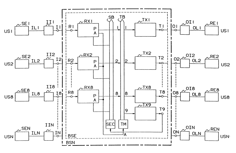
Fig. 1 represents a communication switching system
according to the invention and details of a switching
element BSE used in a switching network BSN of this systen;
Fig. 2 shows an example of this switching network
BSN ;
Fig. 3 rePresents the receive port RX4 and the
control circuit SEC113 of a switching element E113 of Fig.
2 in more detail;
Figs. 4 and 5 show the structure of a Path setup
control cell and of a maintenance cell respectively used in
the system of Fig. 1.
The communication switching system shown in Fig. 1
Z5 is of the tyPe described in the PCT application No
PCT/EP88/00482 (P. Barri et al 4-1) and includes a
multi-stage broadband packet or cell switching network BSN
having a plurality of input terminals Il/N and a plurality
of output terminals 01/N, as well as a pluralitY of user
stations US1/N or outside nodes each comprising a sender
equipment SEl/N and a receiver equipment REl/N. The sender
equipments SEl/N are coupled to the inPut terminals Il/N of
BSN via respective asYnchronous time division (ATD) or
asynchronous` transfer node (ATM) inPut transmission links
ILl/N and respective inPut interface circuits IIl/N. The
2Q10393
-- 4
outPut terminals 01/N of BSN are coupled to the receiver
equipments REl/N through resPectiVe output interface
circuits OI/N and respective ATD or ATM output transmission
links OLl/N.
Each of the user stations includes a traffic
measurement equipment of the tYPe described in the PCT
application No EP88/01037 (P. Joos - W. Verbiest 2-4).
In the cell switching network BSN the N input
terminals Il/N are couPled to the N output terminals 01/N
via a number of cascaded stages of switching elements or
inside nodes of which onlY one, BSE, is shown in relative
detail. This switching element has 8 input terminals Rl/8
connected to respective output terminals of a preceding
stage via multiplex inPut links (not shown) and 8 outPut
terminals Tl/8 connected through multiPlex output links
(not shown) to resPective input terminals of a following
stage (not shown). This means that the switching element
BSE may be considered as hàving 8 bidirectional terminals
Rl/Tl to R8/T8 each connected to a bidirectional multiplex
Z0 link on which a plurality of communication Paths maY be
multiplexed. Inside the switching element BSE the input
terminals Rl/8 are connected to respective input or receive
ports RXl/8 which have a cell output P and an address
output A and which are further connected through an
interconnection bus SB to a switching element common
control circuit SEC. The cell outputs P are connected to
inputs 1/8 of a Time Division Multiplex (TDM)
interconnection bus TB which is controlled by a control
unit TM to which the address outputs A of the receive ports
RXl~8 are connected. Eight outputs 1/8 of the bus TB are
connected through respective output or transmit ports TXl/8
to respective output terminals Tl/8 and a ninth outPUt 9 is
connected to the control circuit SEC via a transmit Port
TX9 having terminal T9.
An example of the switching network BSN is
2~10393
represented in Fig. Z and is also of the tYpe disclosed in
the first above mentioned PCT application. It is a folded
one, with both the inPut and output terminals on one ~left)
side and a mirror plane at the other (right) side. Between
a terminal used as inPut and the mirror plane, BSN is a
distribution network where the path selection maY be
performed freely, whereas between the mirror plane and a
terminal used as outPut it is a routing network wherein the
path is predefined. A path selected in the distribution
network may be extended in the routing network to any of
the outputs. The switching network BSN includes three
stages of switching elements whose terminals 1/8 each
represent both a receive terminal Rl/8 and a transmit
terminal Tl/8. These three stages of switching elements
can be used to interconnect a terminal used as inPut with a
terminal used as output through as manY as five stages.
While the third stage on the mirror side comprises four
groups G31 to G34 each with fo4r elements E311/314 to
E341/344, the first and second stages each include eight
grouPs each also with four elements. Merely to illustrate
a possible connection through five stages, the grouPs of
the first stage have been labelled Gll to G14 and G51 to
G54 and likewise for GZl to G24 and G41 to G44 constituting
the second stage. Thus, with onlY groups Gll, G21, G31,
G34, G44 and G54 shown on Fig. 1, a possible 5-stage
connection involving links L2, L3, L4 and L5 passes through
Gll and G54 both of the first switching stage but Gll being
used as the first stage of this particular connection and
G54 as the fifth. Likewise for G21 and G44 both of the
second switching stage but with G21 as the second stage of
this particular connexion and G44 as the fourth. But such
5-stage connections in a folded network maY also involve
only Gll to G14 or only G51 to G54 in the first stage and
likewise for G21 to G24 or G41 to G44 in the second. The
interconnection between the groups and the elements is such
2010393
that the first grouP of the first stage can only access the
first grouPs of the second stage and likewise for the
remaining 7 grouPs in these two stages. For each such pair
of groups, each of its 4 elements has access to the 4
elements of the Paired grouP. Since there are only 4
groups in the stage, the 8 terminals of each of its 4 x 4
switching elements can be associated with 4 terminals of
each of the 8 groups of 4 switching elements of the second
stage also on a one to one basis, each element of the
second stage having access to all groups of the third stage
and vice-versa.
Fig. 3 shows for such a switching element as E113 in
Fig. 2, the essential parts of its receive port RX4 and of
its control circuit SEC113.
The receive port RX4 includes a receive buffer
RBUF4, a processor RPR4, a routing table RT4, an interface
circuit IC4, a Packet multiplexer PMUX4, an address
multiplexer AMUX4 and a calculation circuit CC. The above
mentioned bus SB is connected to the interface circuit IC4
which has access to the processor RPR4 and to routing table
RT4 and the latter table is couPled to the Processor RPR4
which has access to the buffer RBUF4 and to the calculation
circuit CC. The buffer RBUF4 has a cell input R4 and a
cell output P which is connected to an inPUt of the cell
multiplexer PMUX4 whose outPUt is connected to the
calculation circuit CC. A cell output P of the interface
circuit IC4 is connected to another inPut of PMUX4. The
processor RPR4 and the interface IC4 further have address
outputs A which are connected to resPective inputs of the
address multiplexer AMUX4. The multiplexers PMUX4 and
AMUX4 are controlled bY the interface circuit IC4. The
outputs P of the calculation circuit CC and A of the
multiplexer AMUX4 constitute the outputs of the receive
port RX4.
The switch element control circuit SEC113 includes a
- 2010393
processor PR113 and an associated memory MEM113 which
includes, amongst others, tables Tl to T5. The contents of
Tl to T5 and of the above routing table RT4 will be
described later.
In the present sYstem cell streams are transmitted
comPrising data cells, control cells, e.g. of the type
described in the first above mentioned PCT application ,
and maintenance cells. In the following only the function
of a path setup control cell, a path release control cell
and a maintenance cell is considered in detail.
The structure of a path setup control cell is
schematically represented in Fig. 4. It includes a header
H and an information field IF. The header H identifies the
cell and includes a header error checking code. In the
information field IF :
T : is the type of cell, e.g. a point-to-point path set
up control packet;
RT : is a routing tag containing for instance five sets of
4 bits. Each set defines a resPectiVe one of the 16
terminals or links of a switching element and the
sets are associated to resPective switching elements
of the five stages via which a connection may be
stablished;
SC : is a selection code indicating for each of the
terminals of RT if the selection thereof has to be
performed freely (FS) or is fixed (F);
LL : are labels identifying the communication paths on the
links of a connection;
RP : is the identity of a return path in the network;
LP : are traffic load Parameters characterizing the
individual bandwidth used by a cell stream, e.g. the
average and variance, as described in the EuroPean
patent application 88202852.5 (W. Verbiest 3) ;
CRC: is a check code which is function of the contents of
the information field IF and used to check the
201C~393
-- 8
latter.
The structure of a path release control cell is not
given in detail but maY be found in the second above
mentioned PCT aPplication.
A data cell includes a header constituted by a label
identifying the virtual communication Path used on the link
on which the cell is transmitted and an information field
which comprises data.
The structure of a maintenance cell associated to a
virtual Path or cell stream defined by its traffic
parameters is schematically rePresented in Fig. 5. It
includes a header H and an information field IF. The
header H is of the same type as of a data cell but includes
a single last bit indicating that a maintenance cell is
concerned. In the information field IF :
T : is the type of maintenance cell;
F : is a field to be modified in the switching element
wherein the cell is processed;
X : is a field containing, amonst others, the identity of
the source of the cell stream and the above mentioned
traffic load parameters LP;
CRC: is a check code which is function of the contents of
the information field IF and used to check the
latter.
Z5 Reference is now made to Figs. 2 to 5 for the
description of the establishment of a virtual communication
path between an originating user station US134 and a
destination user station US823.
To establish such a path the user station US134
launches a path setup control cell (Fig. 4) which, amongst
others which are not considered here, contains the
following fields:
RT : X, X, 8, 2, 3
SC : FS, FS, F, F, F
LL : Ll, X, X, X, X, X
20~0~g3
9 _
RP : X, X, X, X, X
with X = undetermined;
FS = free selection;
F = fixed selection.
This means that for the path to be established the
selection of the output link to be used is free in the
first and second stages of the network, that the output
links 8, 2 and 3 whose identities are stored in the cell
have to be used in the following three stages of this
connection, and that the label Ll is to be used for the
virtual communication path on the link interconnecting
US134 and the first stage of the network.
When this cell is received on the inPut terminal R4
or input link 4 (Fig. 2) of the receive port RX4 of the
switching element E113 (Fig. 3), it is entered in the
receive buffer RBUF4 thereof under the control of the
processor RPR4. This processor reads the header H of the
- packet and a checking circuit (not shown) forming part of
the buffer RBUF calculates the check code for the
information field IF and verifies if it is equal to the
check code CRC of the cell or not. The result of this
check is communicated to the processor RPR4 and when the
latter detects that the header is a data cell this result
is ignored since it then has no meaning, whereas otherwise
it is used to continue or stop the processing of the cell.
To be noted that if the cell were a maintenance cell
the processor RPR4 would enable the operation of the
calculation circuit CC. However, because the cell is a
control cell and supposing that the code check is
successful the processor RPR4 does not enable the operation
of the calculation circuit CC. Instead it performs the
following operations:
- it writes the address 4 of the input terminal or input
link 4 (or R4) on which the cell is received and of
which the corresponding output link has to be used by a
20~03~3
-
- 10 -
return or backward cell, in the first position of the
return path field RP of the cell, so that this field
becomes:
RP : 4, X, X, X, X
and then supplies this cell from RBUF4 to the cell
multiplexer PMUX4;
- via its address output A it applies the address 9 of the
output terminal or output link T9 of the transmit port
TX9 to the address multiPlexer AMUX4;
The processor RPR4 then controls the interface
circuit IC4 in such a way that the latter oPerates the
! multiplexers PMUX4 and AMUX4. As a consequence, from these
multiplexers the path setuP cell is supPlied via the output
P to the input 4 (not shown) of the bus TB and the address
is communicated via the output A to the control unit TM of
this bus TB. As a result the control unit TM connects the
input 4 of TB to the transmit port TX9 and transmits the
cell thereto. The latter port then routes the cell to the
switching element control circuit SEC113 via its output T9.
Upon the receipt of the path setup control cell in
the control circuit SEC113 the Processor PR113 thereof
performs the functions described hereinafter.
This processor PR113 selects an output terminal or
output link of the switching element E113, e.g. T8 or 8, on
which the path setup cell J and later the data cells of the
cell stream following it, have to be transmitted to the
second stage or node of the switching network.
In the waY described in the above EuroPean patent
application the processor PR113 calculates the new bandwith
on this link bY means of the previouslY calculated
bandwidth value Bl(8) or load counter value stored in table
Tl of the MEM113 and the traffic load parameters LP
contained in the cell. It then checks if the newly
calculated bandwidth or new load counter value is smaller
or larger than the maximum allowable bandwith B~8) also
20~03g3
stored in table Tl of the MEM113 and accordingly allows the
control cell to be multiplexed on the selected output link
8 or refuses to do so. In the latter case the processor
selects another output link and performs similar
calculations, etc. In this way either a suitable outPut
link, i.e. a suitable virtual communication path thereon,
is found or not and in the latter case the switching
element E113 is considered to constitute a blocked end for
the communication under consideration. In the following it
is supposed that E113 is not a blocked end and that output
link 8 may be used.
Under this assumPtiOn the processor PR113 selects in
MEM113 a new label L2 to indicate the selected virtual
communication path on this outPUt link 8. The processor
PR113 also writes in the routing table RT4 of the receive
port RX4 the routing information or relationship Ll, L2, 8,
El linking the input communication path with label Ll on
- input link 1 with the outPut communication path with label
L2 on output link 8 and with a busY/idle bit El on 1
indicating that the virtual path is busY (otherwise this
bit is on 0~. This happens via the bus SB and the
interface circuit IC4 of this port. The processor PR113
also stores the bit El in the table T2 of its memorY MEM113
at a location having the coordinates R4, Ll.
Finally, the processor PR113 also modifies the
contents of the path setup cell by writing 8 and L2 in the
first positions of the fields RP and L resPectivelY, by
changing FS in the first position of SC by F and by then
subjecting RT and SC to a circular shift in anti-clockwise
direction. Thus the fields of the cell become :
RT : X, 8, 2, 3, 8
SC : FS, F, F, F, F
LL : L2, Ll, X, X, X, X
RP : 4, X, X, X, X
The thus modified cell and the address 8 are then
2010393
- 12 - F
transmitted via the bus SB to one of the receive ports
RXl/8 e.g. to RX4 and more ParticularlY to the interface
circuit IC4 which suPPlies the cell to the cell multiPlexer
PMUX4 and applies the address 8 to the address multiplexer
AMUX4 via its outputs P and A resPectivelY. Under the
control of IC4 the cell is then transmitted from these
multiplexers and via the bus TB to the transmit Port TX8.
By this transmit Port TX8 it is afterwards transmitted on
the output link 8 of E113 to the input terminal 3 of the
switching element E214 where operations similar to those
described above are executed, etc. TherebY the fields RT,
SC, LL and RP of the cell are modified as follows in the
switching elements or inside nodes EZ14, E314, E444 and
E542 if these nodes are not found to be dead ends and
before being transmitted therefrom to a following node :
RT : 82385; 23858; 38582; 85823
SC : FFFFF; FFFFF; FFFFF; FFFFF
LL : L3L2LlLXXX; L4L3L2LlXX; L5L4L3L2LlX; L6L5L4L3L2Ll
RP : 34XXX; 134XX; 5134X; 85134
In this way the point-to-Point virtual Path shown in
Fig. 2 has been established. To be noted that this
connection is similar to that described in the first above
mentioned PCT application. This connection is as follows:
user station US134, link IL134 on which the communication
25 label L1 is used, II134, R4 and T8 of E113, output link 8
on which the label L2 is used, R3 and T5 of E214, output
link 5 on which label L3 is used, R1 and T8 of E314, output
link 8 on which label L4 is used, R5 and T2 of E44, output
link 2 on which label L55 used, R8 and T3 of E542, OI823
and output link OL823 on which label L6 is used.
From the above it follows that subsequent to the
successful transmission of a virtual path setup control
cell using the input link R4 and the outPut link 8 element
E113 the tables RT4, T1 and T2 store the following
information relating to this virtual path :
, _ 2010393
- 13 -
- RT4 stores Ll, L2, 8, El with El = l;
- T1 stores the newlY calculated bandwidth or load counter
value Bl(8)for outPut link 8;
- T2 stores the busy/idle path bit El = 1 in a location
determined by the coordinates R4 and Ll.
In a similar way as described above other virtual
paths are built up through the switching network, as a
~consequence of which the routing tables of the receive
ports as well as the tables Tl and T2 in the memory
circuits of the common control circuits of the switching
elements are updated. As an example, the routing table RT4
and the tables Tl and T2 of the memory MEM113 of the SEC113
for instance store the following information :
RT4 : Ll, L2, 8, El with El = l;
L7, L8, 8, EZ with E2 = 1
for virtual paths using the output link 8 of E113;
L9, L10, 4, E3 with E3 = 1
for a virtual path using the output link 4 of E113.
Tl : Bl(l) to Bl(8)
together with B(l) to B(8) the allowable
bandwidths;
T2 : El = 1, E2 = 1 and E3 = 1 in the locations having
coordinates R4, Ll; R4, L7 and R4, L9 and E = 0 in
the other locations.
After the establishment of the above virtual paths,
data cell streams are transmitted thereon by the user
stations. In each of these stations the traffic
measurement eqUiPment included therein checks for each cell
stream if the corresponding traffic load parameters on the
basis of which the multiplexing of this cell stream on an
output link was allowed are respected. This traffic
measurement equipment also adapts the cell streams if
required, e.g. by dropping cells. By proceeding in this
way it is ensured that the traffic load parameters reflect
the exact traffic load and vice versa.
- 14 - 2 O1 O3 93
With the purpose of checking the correctness of the
various load counters stored in the tables Tl of the
memories of the various control circuits each of the user
stations from which virtual paths have been established
transmits on each of these paths a series of maintenance
cells at a predetermined frequency. These maintenance
cells are interleaved with the Path setup cells. The
frequency and the length of a measurement time interval are
so chosen that in each control circuit associated to a
switching element and with a verY high probability, i.e.
with a negligible loss, at least one maintenance cell is
( received on each of the virtual paths using this switching
element.
As an examPle, when the maximum rate of the
maintenance cells is for instance equal to 100 per link and
per second and when the number of virtual paths per link is
equal to 8000, then the time to transmit one maintenance
cell on each of these paths is equal to T=80 seconds. One
may then calculate that for instance for a switching
element having 16 inPut/outPut links the measurement
interval should be taken equal to 4T in order that the
probability of loss of a maintenance cell in these links
during this interval should be negligible. To be noted
that the measurement intervals follow one another in a
continuous way and are each initiated by the processor
PR113.
Each such maintenance cell transmitted on a virtual
path contains the traffic load parameters LP defining the
individual bandwidth of the cell streams on this path.
Because these parameters are monitored by the traffic
measurement equipment theY are indicative of the real
bandwidth used on this path. For instance, the user
station US134 (Fig. 2) generates a series of maintenance
cells for each of the virtual paths on the inPUt link R4 of
the receive Port RX4 of the switching element E113, these
2010393
- 15 -
virtual Paths being defined in the routing table RT4.
At the start of each measurement interval the
processor PR113 forming part of E113 coPies the load
counters Bl(l) to Bl(8) of the switch element E113 and the
E-bits of all the virtual paths on the input links of this
element from the tables Tl and T2 into the tables T3 and T4
respectively. It also resets all the so called auxiliary
or shadow load counters SBl(l) to SBl(8) stored in a table
T5. These measures are taken in order that the bandwidth
re-calculation operation should be independent from changes
of the virtual paths and therefore also of the bandwidth
used on the links.
In connection with the above it should also be noted
that as long it is stored in the routing table RT4 or T2, a
Path bit E indicates that the corresPonding virtual path is
busy (1) or idle (0), whereas when it is stored in the
table T4 it indicates that a maintenance cell received on
the corresponding virtual path has to be Processed (1) or
not (0) by the processor PR115.
As an example, the function of the first of a series
of maintenance cells relating to the virtual Path Ll, L2,
8, El defined in the routing table RT4 and received during
a measurement interval is considered.
When this first maintenance cell is received in the
receive buffer RBUF4 its check code CRC is verified in the
same way as described above for a path setup control cell.
However, if this check is successful the processor RPR4
upon detecting from the last bit of the header of this cell
that a maintenance cell is concerned consults the routing
table RT4 bY means of the label Ll contained in the header
and uses this information
Ll, L2, 8, El
as follows :
- it substitutes L2 for Ll in the cell header;
- it inserts the identity R4 of the inPut link in this
r - 2o~0393
- 16 -
information and writes the following data
Ll, R4, 8, El
in the field F of the cell, Ll, R4 and L2, 8 define the
virtual paths on the inPut and outPut links
respectively;
- it then applies the thus obtained cell to the inPut P
of the cell multiPlexer PMUX4;
- it operates the calculating circuit CC in order that it
should calculate a new check code for the information
field IF and substitutes this code for the old one.
Such a calculation is required because the F-field of
( the cell has been changed;
- it applies the addresses of the output links 8 and 9 of
the transmit ports TX8 and T9 to the input A of the
address multiPlexer AMUX4.
The processor RPR4 then controls the interface
circuit IC4 in such a way that the latter operates the
multiplexers PMUX4 and AMUX4. As a consequence the
maintenance cell is suPPlied via the outPut P to the inPUt
4 of the bus TB and the addresses 8 and 9 are communicated
via the output A to the control unit TM of this bus. As a
result the control unit TM connects the input 4 of TB to
the transmit ports TX8 and TX9. The transmit port TX8 then
transmits the cell to the following switching element E214
( Z5 via its output T8, whilst the transmit port TX9 supplies
the cell to the switching element control circuit SEC113
via its output T9.
In the switching element E214 the maintenance cell
is processed in a similar way as in the switching element
E113 and this processing will therefore not be described
further. But it is clear that by proceeding in this way
the maintenance cell will finally be transmitted to the
destination station if the path is not interruPted. In
other words the maintenance cell may be used for an
end-to-end verification of the path continuity.
2~10393
1 7
The maintenance cell supPlied to SEC113 is stored in `
the memory MEM113 thereof and is then locally processed by
the processor PR113. More particularly, the latter uses
the information R4, L1 stored in the F-field of the cell to
address the table T4 and to find therein the corresponding
E-bit, i.e. E1 = 1. Because this bit is on 1, as the
maintenance cell is supposed to be the first maintenance
cell transmitted on the virtual path L1, L2 using the links
R4 and 8, the processor PR113 processes this cell. More
particularly, it re-calculates the total bandwidth used on
the outPUt link 8 from the individual bandwidth defined by
( the traffic parameters LP contained in the X-field of the
cell and from the Previously calculated bandwidth stored in
the auxiliary load counter SBl(8) associated to this outPut
link 8 and found in the table T5 by means of the identitY 8
of the output link stored in the F- field of the cell.
PR113 stores the cumulative sum obtained in this auxiliarY
load counter SBl~8-~ associated to the output link.
Afterwards the processor PR113 resets the bit El to 0, thus
indicating that on the virtual path Ll, L2, R4, 8 a first
maintenance cell has been received and processed and that
further maintenance cells on this path are not to be
processed.
In a similar way the load counter SBl(8) is again
( 25 updated upon receipt, during the measurement interval of
the first maintenance cell on the virtual path L7, L8, 8,
E2 including the output link 8, and the load counter SBl(4)
is updated uPon receipt, during this interval, of the first
maintenance cell on the virtual path L9, L10, 4, E3
including the outPut link 4. Also the bits E2 and E3 are
then reset in the table T4 thus indicating that a first
maintenance cell has been received on these virtual paths
and that further maintenance cells received on these Paths
should not be processed.
In the course of a measurement interval it may
- 18 -
2010393
haPpen that a virtual Path is added or released and in both
cases the contents of the tables Tl and T2 are updated. In
the first case no updating of the tables T3~4~5 is required
since the uPdating will take place during a following
measurement interval. On the contrarY, in the second case
precautions have to be taken because the individual
bandwidth of the released path on the one hand is already
included in the total bandwidth information stored in the
third table T3 and on the other hand it has not yet been
taken into account for uPdating the corresponding auxiliary
load counter when the corresponding E-bit is still on 1.
( Also because of the path release no maintenance cells will
be received.
For this reason the path release cell in addition to
its path releasing function performs the same function as a
maintenance cell in the tables T3~4~5. This is described
hereafter.
Such a path release cell is generated in the manner
described in the first above mentioned PCT aPPlication when
a dead end of a virtual path is detected in a node and is
interleaved with the maintenance and path setuP cells. The
path release cell contains the individual bandwidth
information defined by the traffic parameters LP. Upon its
receipt in e.g. the above receive port RX4 the processor
RPR4 thereof inserts the identity R4 of the inPut link in
the cell and routes it to the control circuit SEC113 in a
waY similar to that described above for a maintenance cell.
If the corresponding E-bit is in the set condition the
processor PR113 then increases the contents of the
auxiliary load counter SBl(8) in table T5 by the individual
bandwidth of the cell and resets the corresponding E-bit in
table T4. In the usual way it also clears the connection
by uPdating the tables Tl, T2 and RT4.
As mentioned above the measurement interval is so
chosen that during this interval - and with a very high
r 19 2010~9~
probability - at least one maintenance cell is received for
each of the virtual paths on all the inPut links of E113.
As a consequence at the end of the measurement interval all
the E-bits of this table should normally be on 0 and the
auxiliary load counters in the table T5 should all be in a
position equal to that of the real load counters Bl(l) to
Bl(8) stored in the table T3 Differences only occur in case
of error, e.g. when the values Bl(l) to Bl(8) are not
correct and~or when the calculation has failed.
At the end of a measurement time interval the
processor PR113 therefore compares each auxiliarY load
( counter value stored in table T3 with the copy of the
corresponding load counter value stored in table T5 and in
case these values are different it algebraicallY adds this
difference to the respective real load counter value stored
in table Tl. Thus this real load counter value is
adiusted.
In case at the end of a measurement time interval
one or more E-bits of table T4 are still on 1 this means
that no maintenance cells have been received for the
corresponding virtual Paths. These paths are considered to
be isolated ones and for this reason the processor PR113
resets these E-bits to zero in both tables RT4 and T2.
When all the E-bits of table T4 are on 0 before the
end of a measurement interval the Processor PR113 maY
either already start the adjustment operation or perform
other functions.
It should be noted that instead of being transmitted
by the user stations the various cells could also be
generated in other terminal circuits such as the interface
circuits.
While the Principles of the invention have been
described above in connection with specific apparatus, it
is to be clearly understood that this description is made
only by way of example and not as a limitation on the scoPe
- 20 - 20~0;~93
of the invention.