Note: Descriptions are shown in the official language in which they were submitted.
201045~
N-PHASE SINEWAVE CONVERTER
BACKGROUND OF THE INVENTION
The disclosed invention is generally directed to DC
to AC converters, and more particularly is directed to a
sinewave DC to AC converter which operates efficiently
over widely varying loads.
DC to AC converters are utilized in power supplies
where the originating power source provides a DC voltage,
and the supply voltage is stepped up or down relative to
the originating power source voltage. DC to AC conversion
provides the AC power which can be then stepped up or
stepped down as required. Known DC to AC converters
include squarewave converters and sinewave converters.
Known sinewave converters include a type sometimes
referred to as Class E power converters which operate at
high efficiencies and with low noise. However, known
Class E power converters operate at high efficiencies only
with fixed loads for which they are designed. Different
loads, or variable loads, such as pulsed loads, create
problems including reduced efficiency, increased noise,
and possibly circuit device failures.
SUMMARY OF THE INVENTION
It would therefore be an advantage to provide a DC
to AC sinewave converter which operates at high efficiency
with different or variable loads.
The foregoing and other advantages and features are
provided by a DC to AC sinewave converter which includes
an FET having its gate terminal coupled to a switching
signal which turns the FET on and off. A bilateral,
~ PD 86207
20 1 045 1
_
unidirectional current conductive circuit couples the drain
terminal of the FET to a resonant circuit that is
responsive to a source of DC voltage, and a clamping
circuit is connected between the bilaterally conductive
5 circuit and the source terminal of the FET for preventing
the drain and source terminals from being reverse biased.
Another aspect of this invention is as follows:
a sinewave converter comprising:
a switching transistor having (a) a control terminal
for receiving a switching signal and (b) first and second
controlled terminals which are controllably coupled by a
conductive path when said transistor is turned on pursuant
to said switching signal;
a resonant circuit responsive to a source of DC
voltage; and
means for conductively coupling said first and second
controlled terminals of said switching transistor to said
resonant circuit and for preventing said first and second
terminals from being reverse biased wherein said coupling
means includes a clamping diode and oppositely conductive,
parallel connecting diodes in series with said clamping
diode.
BRIEF DESCRIPTION OF THE DRAWING
The advantages and features of the disclosed invention
will readily be appreciated by persons skilled in the art
from the following detailed description when read in
conjunction with the drawing wherein:
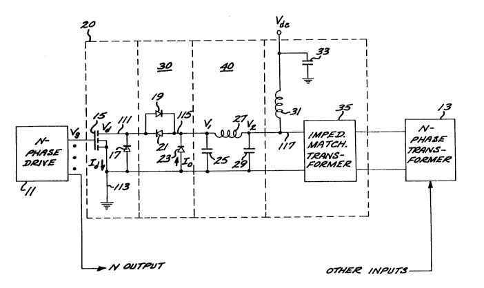
FIG. 1 schematically illustrates a DC to AC sinewave
converter according to the invention.
FIGS. 2A-2F illustrate pertinent voltage and current
waveforms for full load operation of the sinewave converter
of FIG. 1.
FIGS. 3A-3F illustrate pertinent voltage and current
waveforms for light load operation of the sinewave con-
verter of FIG. 1.
`- 201 0451
2a
DETAILED DESCRIPTION
In the following detailed description and in the
several figures of the drawing, like elements are iden-
tified with like reference numerals.
Referring now to FIG. 1, shown therein is a schematic
diagram of a sinewave converter 10 which includes an N-
phase drive circuit 11, which may be a single phase (N=l)
drive circuit. The drive circuit 11 can comprise any of a
number of known drive circuits, and provides N drive
outputs, each havinq a 50 percent duty cycle over the
desired AC operating frequency.
For N greater than 1, each of the outputs of the N-
phase drive circuit 11 will have the same operating
frequency, but are offset by 360/N degrees. Thus, for
example, for a 3-phase system, the drive outputs would be
offset by 120 degrees.
20~045~
Each of the N drive outputs of the N-phase drive
circuit 11 is coupled to a respective switching circuit, a
representative switching circuit 20 being shown in FIG. 1.
The output of the switching circuit 20 is coupled to an
N-phase transformer 13. The switching circuits for other
phases, if any, would be substantially similar to the
switchin~ circuit 20 and would have their outputs coupled
to the N-phase transformer 13.
The switching circuit 20 includes an N-channel power
FET 15 which has its gate connected to one of the outputs
of the N-phase drive circuit 11. The drain of the power
FET 15 is coupled to a node 111, while the source of the
power FET 15 is coupled to a common reference voltage,
which by way of example is shown as a ground node 113.
The cathode of a diode 17 is coupled to the node
111, and the anode of the diode 17 is coupled to the
ground node 113. The diode 17 functions to protect the
FET against excessive voltage.
A diode network 30 is coupled between the node 111
and the ground node 113. The diode network 30 includes
cross coupled diodes 19, 21. The anode of the diode 19
and the cathode of the diode 21 are both connected to the
node 111. The cathode of the diode 19 and the anode of
the diode 21 are connected to a node 115. The diode
network 30 further includes a diode 23,- which has its
cathode connected to the node 115 and its anode connected
to the ground node 113. As discussed more fully herein,
the diode 3 conducts reverse current instead of the body
diode of the FET 15, and is preferably a fast recovery
device.
The switching circuit 20 further includes a C-L-C
resonant circuit 40 coupled between the node 115 and the
ground node 113. The resonant circuit 40 includes a
capacitor 25 coupled between the node 115 and the ground
node 113. An inductor 27 is connected between the node
. PD 86207
2010451
115 and a node 117, and a further capacitor 29 is con-
nected between the node 117 and the ground node 113. The
resonant frequency of the resonant circuit 40 is substan-
tially equal to the frequency of the signal applied to the
gate of the FET 15.
The tank circuit 40 functions as an impedance
matching network, and its elements are selected to provide
a Q greater than one (1), as a result of which the voltage
across the power FET 15 will ring at the resonant fre-
quency of the tank circuit 40 when the power FET 15 is
turned off. That tank circuit particularly matches the
output impedance of the power FET 15 to the load applied
to the N-phase transformer 13, and further forces the
voltage and current transitions (zero crossings) to occur
at different times, thereby reducing transistor switching
loss. The tank circuit 40 also controls the voltage
across the power FET 15 so that at turn-on it does not
exceed a maximum of Von.
The tank circuit 40 is specifically disclosed as a
known design sometimes called a PI circuit, but other
impedance matching networks, such as L and T networks, can
also be utilized. Also, a power bipolar transistor could
be utilized instead of the power FET 15.
The node 117 is coupled to a DC supply voltage
source Vdc via an inductor 31, which is a feed choke and
is large enough to allow a constant flow of current. The
inductor 31 further provides RF isolation for the DC
supply voltage source Vdc. An AC ripple filtering capa-
citor 33 is coupled between the DC voltage source Vdc and
the ground reference node 113.
The voltage V2 at the node 117 varies sinusoidally,
and is out of phase relative to the input to the FET 15 by
greater than 135 degrees but less than 180 degrees.
The input of an impedance matching transformer 35 is
coupled to the node 117 and the ground reference node 113.
~ 07
-- 5 2010451
The output of the impedance matching transformer is
coupled to one input of the N-phase transformer 13.
The operation of the sinewave converter 10 for N
equal to 1 will now be described with reference to FIGS.
2A-2F and 3A-3F which schematically illustrate pertinent
voltage and current waveforms for full load (low imped-
ance) and light load (high impedance) conditions, respec-
tively. The voltage Vg is the voltage applied to the gate
of the power FET 15, while Vd in the voltage at the drain
of the FET 15. The current Id is the drain current of the
FET 15, and the current Io is the current through the
diode 23. The voltage Vl is the voltage at the node 115,
while the voltage V2 is the voltage at the mode 117.
When the voltage Vg at the gate of the FET 15
transitions low, the FET 15 turns off and remains off
while the voltage Vg is low. The voltage Vl at the node
115 rings up (increases) over a time period Tl and then
down (decreases) over a time period T2. During the same
time periods Tl and T2, the voltage Vd at the drain of the
FET also rings up and then down as the parasitic capaci-
tance of the FET 15 is charged through the diode 21 and
then discharged through the diode 19. As a result of the
voltage drop across the diodes 19, 21, the voltage Vd at
the drain of the FET 15 is one diode drop less than the
voltage Vl when it rings up, and one diode drop greater
than the voltage Vl as it rings down.
When the voltage Vl at the node 115 goes negative
during the time period T3, the diode 23 conducts the
current Io, and prevents the voltage Vl from becoming more
negative than one diode drop. As a result, the voltage Vd
at the drain of the FET 15 iS prevented from going below
zero. Thus, the body diode of the FET is prevented from
being reverse biased. If the body diode of the FET 15
were allowed to be be reverse biased to provide reverse
PD 8~r-8,
2010451
conduction, high dissipation and degraded efficiency would
result, as well as possible failure.
When the voltage Vg at the gate of the FET 15
transitions high, the FET 15 turns on and remains on while
the voltage Vg is high during the time period T4. The FET
drain current Id conducts through the inductor 27 and the
diode 21, causing a voltage drop across the FET 15 equal
to the ON-resistance thereof times the drain current. The
voltage V1 is one diode drop above the voltage Vd during
the time period T4.
At the end of the time period T4, the voltage Vg
applied to the gate of the FET 15 again transitions low,
and the foregoing repeats.
The voltage V2 at the node 117 takes on a sinusoidal
shape as the energy supplied by the DC voltage source Vdc
rings around the resonant circuit 40 when the FET is
periodically turned on and off by the voltage Vg applied
to its gate.
With a lighter load, as illustrated in FIGS. 3A-3F,
the time periods Tl and T2 are shorter than with full
load, while the time period T3 is greater. Also, the peak
of the voltage Vd at the drain of the FET 15, while it is
off, is greater than with full load. The drop across the
FET 15, while it is on, is less.
The clamping action of the diode 23 prevents the
body diode of the FET 15 from being reverse biased,
thereby preventing highly dissipative reverse conduction,
which is particularly significant at lighter loads.
Without the clamping action, the FET 15 would be sub~ect
to reverse current during the time period T3, which as
discussed above increases with lighter loads. Thus,
reasonably constant high efficiency, on the order of 92-95
percent, is provided over widely varying loads. As a
result of the high efficiency, operating frequencies as
high as 10 MHz can be utilized.
PD 86207
7 201045~
The following are examples of operating parameters
and component values for the disclosed sinewave converter.
The frequency of the signal applied to the gate of the FET
15 is denoted Fs, while the peak voltage across the FET is
denoted Vp.
Vdc : 140 Volts DC
Fs : 1 MHz
Vp : 420 V
FET 15 : International Rectifier IRF450
Diode 17 : Micro Semiconductor IN6173
Diode 19 : SEMTECH IN6081
Diode 21 : SEMTECH IN6081
Diode 23 : Solid State Devices SDR 3K
Inductor 27 : 1.35 microHenrys
Inductor 31 : 3.5 microHenrys
Capacitor 25 : 18.4 nanoFarads
Capacitor 29 : 12.5 nanoFarads
Capacitor 33 : .05 microFarads
While the foregoing has specifically disclosed the
use of a power FET, a power bipolar junction transistor
could also be utilized, which may require different values
for the capacitors 25, 29 and the inductor 27 of the
resonant circuit 40.
The foregoing has been a disclosure of a DC to AC
sinewave converter which operates at high efficiency with
variable loads and over a wide range of loads. The
sinewave converter also provides the advantages of low
harmonic noise generation, low stresses on the switching
components and therefore greater reliability and low cost.
Also, the radiated noise is reduced and simpler AC filter-
ing can be utilized. The sinewave converter further
allows for higher operating frequencies.
Although the foregoing has been a description and
illustration of specific embodiments of the invention,
various modifications and changes thereto can be made by
P~ 86207
20~0451
persons skilled in the art without departing from the
scope and spirit of the invention as defined by the
following claims.
PD 80~u