Note: Descriptions are shown in the official language in which they were submitted.
2010479
- 1 -
REDUCED-HEIGHT WAVEGUID~TO-MICROSTRIP TRANSITION
Technical Field
The present invention relates to a reduced-height waveguide-to-
microstrip transition, where the microstrip is capacitively coupled to a
5 waveguide, which includes a predetermined width-to-height ratio, by means
of a T-bar conductive pattern formed on one side of a substrate.
De~cription Of The Prior Art
Standard waveguide-to-microstrip transitions have been
developed as shown, for example in U.S. patents 3,518,579 issued to
10 M. Hoffman on June 30, 1~70; 4,052,683 issued to J.H.C. van Heuven et al.
on October 4, 1977; 4,453,142 issued to E. R. Murphy on June 5, 1~84; and
the article by E. Smith et al. in Communications International, Vol. 6,
No. 7, July 1~79 at pages 22, 25 and 26. However, all of these transitions
are used for connecting full-height waveguide to either microstrip of
15 coaxial-line terminals. In certain applications, such as phased-array
systems, where thousands of waveguide horns are packed together,
; reduced-height waveguides are generally selected for small size and reduced
weight. An example of the use of reduced-height waveguides in an array is
disclosed, for example, in U.S. patent 4,689,631 issued to M. J. Gans et al.
20 on August 27, 1~87, where a space amplifier arrangement is disposed in the
` ~ ~ aperture of an antenna. The space amplifier comprises a waveguide array
where full-sized waveguide input and output waveguide sections are each
reduced, via an impedance matching configuration, to a reduced-height
-- waveguide section into which a separate portion of a microstrip amplifier
-` 25 arrangement is extended.
; The problem with providing microstrip-to-reduced height
- ~ waveguide transitions is that the transition should extend into the reduced-
height waveguide section by a distance equal to approximately one-quarter
wavelength of the ~ignal to be intercepted or transmitted by the transition.
30 While the one-quarter wavelength distance is available with standard full-
~-~ size waveguides, the reduced-height waveguides do not provide such
- distance between the more closely spaced opposing broadwalls of the
waveguide. As a result, if the known transitions normally used with full-
sized waveguides were extended through one of such closely-spaced opposing
35 walls of the reduced-height waveguide, such transition would be shorted out
by the opposing waveguide wall of such reduced-height waveguide.
. '~
- 2 - 2010479
Therefore, the problem remaining in the prior art is to provide a
microstrip-to-reduced height waveguide transition that provides the
necessary one-quarter wavelength distance for insertion into one on the
opposing closely-spaced walls of a reduced-height waveguide section without
5 being shorted while being capable of efficient transfer of signals between the microstrip and the reduced-height waveguide section.
Summary of the Invention
The foregoing problem in the prior art has been solved in
accordance with the present invention which relates to a microstrip-t~
10 reduced height waveguide transition comprising the configuration of a T-bar
conductive pattern on one major surface of the microstrip. The T-bar
pattern permits approximately a quarter wavelength distance to be provided
when measured along both the body and an extended arm of the "T"
pattern without the pattern being shorted to a wall of the reduced-height
15 waveguide section when such pattern is extended through an aperture in
the wall of the reduced-height waveguide. Such transitions can also be used
for reduced height waveguide-microstrip-waveguide transitions comprising
the form of a cascaded double-T-bar transition on the microstrip substrate.
Other and further aspects of the present invention will become
20 apparent during the course of the following description and by reference to
the accompanying drawings.
Brief Description of the Drawin~s
FIG.lis a front view of an exemplary structure of a T-Bar
transition disposed on a major surface of a microstrip in accordance with
- 25 the present invention as disposed inside a rectangular reduced-height waveguide;
FIG.2is a side view of the exemplary structure of FIG.l;
FIG.3is a front view of an exemplary microstrip metallization
for a waveguide-microstrip-waveguide transition in accordance with the
present invention;
FIG.4is a rear view of the exemplary microstrip ground plane
metalization for the exemplary transition of FIG. 3;
FIG. 5 is a side view of a waveguide-microstrip-waveguide
transition of FIG. 2 as disposed between two reduced-height waveguide
35 sections; and
.:
--` Z0104,~9
FIG. 6 is a graph of radiation resistance vs. frequency for a
particularly dimensioned T-Bar transition of FIG. 1 when the transition is
; disposed inside a particularly dimensioned reduced-height waveguide. Detailed DescriPtion
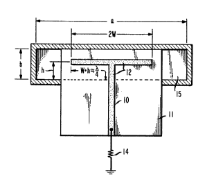
FIGs. 1 and 2 show a front and side view, respectively, of the
structure of a conductive microstrip line 10 terminating in a conductive T-
bar antenna transition pattern 12, with a width "2W", which is formed on a
first major surface of a substrate 11, which substrate can comprise any
suitable material as, for example, alumina. The T-bar transition 12 is used
10 to connect the microstrip transmission line 10, which is terminated in a load- 14, to a reduced-height waveguide section 15 which comprises a width "a"
and a height "b". For exemplary purposes only, it will be considered
hereinafter that microstrip line 10 has a width of 0.062 inches, but it should
be understood that any other suitable line width can be used. Additionally,
: 15 a conductive ground plane 13 is formed on a second major surface of
substrate 11 opposite the first major surface of substrate 11 such that the
ground plane does not extend into the area opposite T-bar transition 12. As
shown in FIGs. 1 and 2, substrate 11 is inserted through an aperture 16 in a
wall of reduced-height waveguide section 15 so that the central conductor
20 forming the leg of T-bar transition 12 extends a predetermined distance "h"
into waveguide 15.
; As shown in the side view of FIG. 2, when substrate 13 is
disposed in aperture 16 of reduced-height waveguide section 15, ground
plane 13 is coupled to the wall of waveguide 15 by any suitable means such
25 as, for example, by contact, while the T-bar transition extends through
3 aperture 16 of waveguide section 15 without contact with a wall of the
waveguide section. It should be understood that ground plane 13 does not
overlap the opposing area to T-bar transition 12 when disposed within
waveguide section 15 so that electromagnetic signals 18 propagating towards
30 T-bar transition 12, or emanating from the T-bar transition, are permitted
to pass through substrate 11. A sliding short 17 is disposed at a distance
~e~ behind the T-bar antenna transition 12 to tune out the antenna 12
reactance and avoid reflections as is well known in the art.
- Radiation resistance is defned in communication dictionaries as35 the electrical resistance that, if inserted in place of an antenna, would
consume the same amount of power that is radiated by the antenna; or the
4 2010479
- ratio of the power radiated by the antenna to the square of the rms antenna
current referred to a specified point. It is known that the radiation
resistance of an open-ended probe antenna inside a waveguide for a
predetermined wavelength is dependent on the free space impedance, the
5 propagation constant of a particular TE mode (e.g., the TElo mode), the
propagation constant of free space, the backshort distance ~e~, and the
width "a" and height "b" of the waveguide. FIG. 6 shows a graph of
exemplary values for the radiation resistance of a first and a second T-bar
antenna transition 12 disposed inside a standard WR-229 reduced-height
10 waveguide section 15 versus frequency.
For an exemplary first T-bar antenna transition, having a half-
width W=0.500 inches and a height h=0.150 inches disposed in a WR-22
reduced-height waveguide section 15 having a width a=2.2~ inches and a
height b=0.200 inches, the exemplary values of the radiation resistance for
15 various frequencies are shown by the "circles" in FIG. 6. It should be noted
that the radiation resistance for the first T-bar transition is 43.5 ohms at 4.0GHz. Fig. 6 also shows exemplary values of the radiation resistance for a
second T-bar antenna transition 12 having a half-width W=0.700 inches
- and a height h=0.150 inches disposed inside a WR-22~ reduced-height
20 waveguide section 15, which exemplary radiation resistance values are
indicated with "X"s for the various frequencies. It should be noted that at
- 4.0 GHz the radiation resistance of the second T-bar antenna transition
equals 50 ohms. Therefore, it can be seen that by increasing the half-width
(W) of the T-bar antenna transition from 0.50 inches, for the first T-bar
25 transition, to 0.70 inches, for the second T-bar transition, the radiation
- resistance was increased from 43.5 ohms to 50 ohms. Such change in
radiation resistance illustrates that there is a trade-off between the T-bar
-~ transition width (2W) versus its height (h), and that a short T-bar
transition can still work if its width is increased. Additionally, it should be
30 understood that by adjusting the T-bar transition 12 width and height, a
good transition between a microstrip line 12 and a reduced-height
waveguide 15 can be designed. For comparison, the waveguide impedance
for a WR-229 reduced-height waveguide, at 4 GHz, is found to equal 69
ohms which is comparable to the radiation resistance of the second T-bar
35 antenna transition above.
.
,
2010479
:,
The present T-bar antenna transition can also be used to provide
a waveguide-microstrip-waveguide transition by cascadirg two of the T-bar
transitions of FIG. 1 in the manner shown in FIG. 3. More particularly, in
the front view of FIG. 3, a first T-bar antenna transition 12a is directly
5 connected to a second T-bar antenna transition 12b via microstrip line 10
on a substrate 11. This type of transition can be used, for example, for
connecting hybrid and monolithic high-speed circuits to reduced-height
waveguide input and output ports. For such use, the first T-bar transition
12l couples microwave energy to or from a first waveguide section and the
10 second T-bar transition 12b couples microwave energy from or to a second
waveguide section. The back view of such waveguide-microstrip-waveguide
transition is shown in FIG. 4 and includes an exemplary metalized
backplane 13 configuration on substrate 11. As stated hereinbefore, the
metallization of the backplane is omitted from the area opposite the T-bar
15 antenna transitions 12a and 12b to permit electromagnetic waves to impinge
the transitions from either side of the substrate 11.
- FIG. 5 illustrates a cross-sectional view of a broadband
waveguide-microstrip-waveguide transition 20, of the type shown in FIG. 3,
disposed between two waveguide sections 21 and 22. Waveguide sections 21
`:~ 20 and 22 are each reduced in height in predetermined steps when traveling
from its associated entrance port to the transition 20 area to provide, for
- example, appropriate impedance matching. In FIG. 5, waveguide 21 is
reduced to, for example, a WR-22~ reduced-height waveguide section in the
area of transition 20 so that electromagnetic signals propagating towards
25 transition 20 are intercepted by T-bar antenna transition 12a. Any signal
passing through the area of T-bar transition 12a in back of substrate 11 will
be intercepted by backshort 17a to tune out any reactance and avoid
reflected signals back to transition 12a. A similar arrangement is provided
for waveguide 22 and T-bar antenna transition 12b. Therefore, any signal
30 propagating from the entrance port of waveguide 21 will be intercepted by
T-bar antenna transition 12a and be transmitted via microstrip line 10 to
T-bar antenna transition 12b for launching into waveguide 22 for
propagation towards its entrance port. A signal entering the entrance port
for waveguide 22 would similarly be propagated to the entrance port of
35 waveguide 21 via waveguide-microstrip-waveguide transition 20.
2010479
-- 6 --
It should be noted that for the arrangement of FIG. 5, the
waveguide-microstrip-waveguide transition is disposed on the side of
substrate 11 facing the entrance port of waveguide 21. In the arrangement
of FIG. 3, it should be noted that the top transition 12a has a width
5 indicated as 2Wa and lower transition 12b has a width indicated as 2Wb.
When the transition of FIG. 3 is used in the arrangement of FIG. 5, the
width of transition 12a would be wider that the width of transition 12b in
order to compensate for the difference in the sliding short 17a and 17b
location. More particularly, the T-bar of transition 12a is disposed on the
1~ reverse side of substrate 11 relative to associated sliding short 17a~ while the
T-bar of transition 12b is disposed facing its associated sliding short 17b.
It should be understood that the above-described embodiments
are simply illustrative of the principles of the invention. Various other
modifications and changes may be made by those skilled in the art which
15 will embody the principles of the invention and fall within the spirit and
;j~ scope thereof.
. :-
:
':
., '
,...
:"
.:,
`:
~. .
. .