Note: Descriptions are shown in the official language in which they were submitted.
;~ 1 BACKGROUND OF THE INVENTION
The present invention relates to a power
signal processing system suitably used with a power
protection system or a control system of a power trans-
mission and distribution system including a power
. ~.
system and a distribution system, and more in particular
to a power signal processing system and a related system
based on multiprocessor system with processing means
optimally distributed into a plurality of units
according to processing functions.
The present invention also relates to a
- protective relay system of a power system comprising
.
~ a plurality of units optimally distributed according
~.
to the processing functions, and more in particular to
; 15 standardization of software for digital protective
relay operation.
- (1) In recent years, a digital relay has been
developed as a protective relay of the power system
to process voltage or current signal data sampled at
regular time intervals, detect a system fault and thus
to protect the system.
,:~
A conventional digital relay of this type, as
disclosed in Journal of the Institute of Electrical
Engineers of Japan, Vol. 105, No. 12, p. 12, infra,
comprises an input section, a processing section,
.; ~
-- 1 --
2a~7~
1 a setting section and an output section. The input
section of this relay includes a filter, a sample-hold
circuit, a multiplexer, an analog-digital converter
and a buffer. Also, the processing section includes a
5 CPU (microprocessor), a RAM and a ROM for relay
computation. In this case, a plurality of relay
functions are executed by CPU in time division multi-
plexing mode.
In another similar digital relay system current
; 10 and voltage signals are supplied from a current trans-
former CT, a transformer PT and the like arranged on
a transmission line L, and undergo computations accord-
ing to a predetermined algorithm thereby to monitor the
system for an accident. If an accident like the
15 grounding occurs in the transmission line L, this
system receives the resulting variations in current and
voltage signals, makes a computation on the basis of
these signals, pinpoints a position of fault, and
produces a signal for tripping a circuit breaker at
20 optimal position.
A higher-graded protective performance, higher
speed and greater accuracy are now required in order
to meet the more and more complicated phenomena of
system accidents. A multitude of data are required
25 to be processed at high speed according to various
algorithms.
The above-mentioned type of digital relay,
however, is limited in the processing ability of the
2Q~37 ~
1 processing section thereof, and is hardly unable to
meet the great data processing requirements. An
unavoidable measure is to arrange a plurality of digital
relays in juxtaposition, thus posing the problem of
a generally bulky system configuration.
Such a system, being an assemblage of a
; plurality of independently-functioning digital relays,
is not easily able to secure cooperation among them.
For example, it is difficult for the relays to share
the results of operation. Separate executions of
.~
operations are unavoidable for the respective relays,
thus leading to the problem of low efficiency.
A multiprocessor system for executing the
operation by a plurality of microprocessors has also
been suggested.
In this type of system, as disclosed in JP-
A-60-84912, the protective operation is divided into a
plurality of individual processing operations for
protective relay elements, respectively, which
individual processing operations are executed by
independent operation modules connected by a serial
data transmission line. Each operation module receives
- only the data required by itself as an input, and after
accomplishing an assigned operation, transmits its
output to the serial data transmission line.
` Another digital protective relay system for
-~ power applications is disclosed in the 1986 National
~ Conference Report No. 1319 of the Institute of Electrical
2 ~ 7 ~
1 Engineers of Japan. In this system, the functions
related to the protective relay are divided into a
plurality of units respectively packaged on different
printed boards, which are connected through a system
bus. The units are divided depending on functions
into an analog input, computation, setting, accident
detection, power supply, input converter, indication,
output, input and an auxiliary relay sections.
of all the aforementioned conventional systems,
the system configured of a plurality of operation
modules has the protective operation divided by element,
and each protective operation thus divided is processed
as a pipeline system separately.
The data transfer by a serial transfer line,
however, consumes considerable time, and the requirement
` of serial-parallel conversion at each module increases an
processing overhead. This conventional system, there-
fore, lacks a sufficient processing ability for a
,
: protective relay requiring the real-time processing of
a great amount of data. Also, a relay system having
a multiplicity of elements requires a multiplicity of
processing modules, resulting in a bulky system. The
great time taken for data transfer among modules, on
the other hand, makes high-speed processing difficult.
The digital relay disclosed in the Journal
of the Institute of Electrical Engineers of Japan,
in spite of its protective relay functions divided into
~; a plurality of units, fails to take into consideration
-- 4 --
2~c37 iL
1 the appropriate control of timings and the like of
operation and data transfer between the units.
Specifically, in the case where data transfer
is to be executed between a given unit and another unit,
.
each unit is required to secure the right to use the
bus and execute the control operation to see whether
communications between the units is possible. This
not only complicates the control operation but also
requires an additional function of each unit for the
" 10 particular purpose, thus posing the problem of an
` increased overhead. In addition, if the bus is occupied
by another unit, it is necessary to defer data transfer.
This is a problem not negligible for a relay system
for power applications requiring the processing of
a great amount of data in a short time.
Further, these control functions, which are
provided for each unit to meet the system configuration
` and are different from one system to another, are
difficult to standardize.
What is more, in expanding an existing relay
. system, it is necessary to set the control functions anew
for each unit. This renewed setting is effected by
rewriting the control program of the microprocessor
of each unit, and the rewriting of the control programs
of all the microprocessors takes considerable time and
labor. Since it is necessary to prepare each control
program taking the characteristic difference between
the unit functions into consideration, the problem of
~ ~.
2 ~
1 of a narrow capacity of expansion is posed.
Also, the use of the microprocessor in the
processing operation imposes a limit on the processing
capacity of the unit in high-speed operation. Seeking
- 5 a high speed would sacrifice the accuracy, and vice
versa. If the processing capacity is to be improved,
on the other hand, many units are unavoidably added.
- Adding units in the system, however, gives rise to
- various problems as described above.
- 10 Another conceivable method of improving the
general processing capacity may be to use a plurality
of systems in parallel. The scale of the whole system
configuration would be increased, accompanied by an
increased power consumption and cost. Also, because
the smooth cooperation among the systems is not an easy
matter, the lower reliabil~ty would be unavoidable in
the functions requiring the cooperation among parallely-
- operated systems, thereby making it difficult to realize
high functions.
. .
Furthermore, the generally low reliability
of the analog input section would make it indispensable
to switch the input signal to a check signal for
inspecting all the channels at regular intervals of
time (say, once every day) in order to improve the data
- 25 reliability. This requirement is conventionally met
- by adding a special check circuit. This results in an
increased volume of hardware and a complicated software
processing, thus providing a bottleneck against an
-- 6
2 ~ 7 ..
1 improved reliability.
(2) Another conventional digital relay is disclosed
in the Journal of the Institute of Electrical Engineers
; of Japan (Vol. 105, No. 12, p. 1158 to p. 1160) and
Hitachi Hyoron (Vol. 63, No. 4, April 1981, p. 52 infra).
This digital relay comprises an input section, a
computation processing section, a setting section and
an output section. The input section generally has
a 12-bit A/D converter, and a 16-bit microprocessor
(MPU) is used for processing the relay operation. This
; MPU is of what is called fixed point arithmetic type.
Also, the software (operation technique) relating to
the protective relay operation is realized by time-
division multiple processing of the operations of a
~, 15 plurality of types of protective relays (including
a reactance relay, a mho relay and an offset relay).
The product computation technique is generally used as
a computation algorithm as disclosed in the latter
publication.
~ 20 The above-described conventional systems,
`~ in which the operation programs relating to a plurality
-~ of protective relays are prepared separately from each
other, has the problem of the long time required for
preparing operation programs for an inferior software
` 25 productivity and a great program capacity required.
This problem is also attributable to the fact
that a 16-bit processor of fixed point arithmetic type
is used for operation and the processing speed for
-- 7 --
2 ~ 7 ~
1 multiplication is low.
In the 16-bit processor of fixed point
arithmetic type, the processing for securing a pre-
determined number of significant digits is complicated
with the increase in multiplication commands, and the
. program is required to be modified depending on the
number of relay settings.
Further, the limited program capacity and
- limited execution time leaves something unsatisfied in
. 10 respect of accuracy as the program cannot be prepared
: ~ in high accuracy.
. SUMMARY OF THE INVENTION
Accordingly, it is an object of the present
; invention to provide a power signal processing system
which is compact and.meets various system requirements
including expandability, versatility, high functions
~ and multiple functions by unit addition or exchange in
order to cover the whole series of equipment including
a transmission line, a bus, a transformer, a power
generator, a voltage regulator and a stationary reactive
power compensator covering a wide range of the power
system including voltage classes of 500 kV to 6.6 kV.
: Another object of the present invention is
` to provide a power signal processing system for improving
the digital processing capacity of the units remarkably
(high-speed processing) and realizing high-speed and
high-accuracy processing functions without increasing
2 ~ 7
,~
1 the system size.
Still another object of the present invention
is to provide a compact, reliable and high-performance
power signal processing system in which the unit
functions are optimally divided and the processor is
mounted on each unit for an improved diagnostical
function and an improved system reliability free of the
automatic check function with a check input applied by
way of an analog input section of the system.
A further object of the present invention is
' to provide a method of protective relay operation and
a protective relay system which obviates the problem
:'
;~ specified in (2) above and facilitates the preparation
of an operation program for an improved software
productivity.
According to one aspect of the present inven-
tion, there is provided a power signal processing system
- in which a series of processing operations from receiv-
ing to production of signals based on processing are
executed by a plurality of units divided according to
the processing functions, and the data transfer between
the units is controlled by a system control unit to
execute the series of processing operations by processing
function sequentially.
According to another aspect of the present
invention, a digital signal processor is mounted on
the high-speed processing unit of all the units for
dividing and executing the processing functions thereby
- _ g _
2 ~ 7 ~
1 to permit the high-speed processing operation.
- According to still another aspect of the
present invention, a series of processing function
from the receiving to production of signals based on
the result of processing operation in this power signal
processing system are preferably divided into individual
units including ~ system control, ~ analog input,
protective operation (relay operation) or control
operation, ~ sequence processing, ~ setting and
indication, and ~ digital input and output. Also,
an independently-operable accident detection unit is
desirably added to assure a fail-safe function.
These units are preferably configured as
follows:
(1) The units ~ to ~ and ~ have mounted
a processor thereon.
(2) The units ~ to ~ are connected through
a general-purpose bus, or preferably, a bus of world
standard like a multi-bus or VME bus, for example.
~3) The digital input/output unit ~ above is
connected with the sequence processing unit ~ by way
of a bus different from the general-purpose system bus.
(4) The accident detection unit ~ should be
arranged in completely separate hardware from the units
- 25 ~ to ~ in order to avoid mutual interferences.
Further, in order to achieve the object of
high-speed processing operation, the units ~ to ~
have a processor mounted thereon, and the analog input
-- 10 --
2~57~
1 unit ~ and the protective (control) processing unit
~ , in particular, have a digital signal processor DSP
capable of high-speed processing operation mounted
thereon. The other units have a general-purpose
~ 5 microprocessor mounted thereon. The units ~ to ~
- are adapted for parallel operation. Specifically, the
system control unit ~ controls the data to be
sequentially transferred to each unit thereby to control
~-` the units for performing a series of processing
operations in cooperation.
According to another aspect of the present
invention, there is provided a power signal processing
system in which each processing unit includes a memory
enabling the particular processing unit to be accessible
to other units, and a data set beforehand is written in
this memory by the particular unit or other units
periodically, which data is read periodically by another
unit, so that it is decided whether the data thus read
- is the one set beforehand thereby to monitor the
operating conditions of the unit.
Further, in view of the fact that each unit
has a processor mounted thereon, a fault of a given
unit may be detected by self check in addition to the
mutual check mentioned above.
Furthermore, a check signal for hardware check
may be always superimposed on the analog input signal,
and this check signal may be reduced to a value not
affecting the system performance by a digital filter,
:: 2~ 7~
1 so that the resulting signal component may be extracted
by a digital signal processor in the analog input unit,
thus checking the normality of the analog input section
all the time.
- 5 The above-mentioned features of configuration
lead to the functions and effects of the present inven-
tion described below.
The processing functions relating to the
protection or control of a power system are realized
by appropriately selecting and combining the units
~ to ~ . Also, in view of the fact that data transfer
between the units is controlled by a system control
unit, all that is required in constructing a system
is to set a system control unit to meet the system
; 15 requirement for transfer control and to connect units
having the required functions in the required number.
It is thus possible to standardize the system.
For example, a system having each one of the
units ~ to ~ mentioned above may be standardized
as a basic system. In the case where a system to be
built has many channels of input data, an analog input
unit may be added. If such a system has a great proces-
sing volume, on the other hand, a computation processing
unit may be added to meet the requirements.
The signal processing system according to
the present invention, therefore, permits development
of a system configuration in a wide variety of applica-
tions. It is thus possible to build a system capable
7 ~
1 of protecting or controlling various objects including
the transmission line, transformer, generator and bus
in a wide range of voltage classes such as from 500 kV
;~ to 6.6 kV.
Besides, the ease with which the units may be
increased or decreased in number or modified realizes
a compact, reliable digital protection (control) system
of multiple and high functions and performance.
Specifically, a system configuration high in versatility
and flexibility is produced.
Also, if a digital signal processor (DSP)
capable of high-speed computation is mounted on the units
and ~ , the following advantages are attained.
1) The high-harmonic components generated in the
system are removed by a digital filter with DSP, realiæing
a compact, reliable analog input unit ~ with the
performance (accuracy, stability) several times (twice
~` or thrice) higher than in the prior art.
; 2) The computation relating to the protection or
control of the power system is processed within a short
time, and a DSP of floating point arithmetic type widens
` the dynamic range, eliminating the labor which otherwise
might be required for scaling or the like. Further,
the high processing speed makes possible many (multiple)
functions and high performance operation, thus contribut-
ing to an improved performance in control and protection
characteristics (high accuracy, and high speed
- operation), as well as reducing the size and cost with
.
~ - 13 -
,,
.
2 ~
1 an improved reliability.
In the case of the units ~ to ~ , on the
other hand, parallel operation free of overhead is made
possible by full use of the computation period of a
processor mounted thereon, and therefore the processing
capacity of each unit, that is, the system (throughput)
is improved.
In addition, if a high-speed DSP is applied
to the unit ~ and high harmonics generated in the
power system are eliminated by a digital filter, it is
possible to realize a characteristic free of charac-
teristic variations of a resistor or a capacitor (high
accuracy) and stable (free of secular variations or
the effect of temperature changes) as in a well-known
- 15 analog filter.
Further, the DSP of the unit ~ reduces the
check or monitor signal superimposed on the analog
input signal to such a degree as not to adversely
; affect the performance relating to the protection or
control of the power system and at the same time checks
the amplitude and frequency of the check and monitor
signals constantly. As a result, the conventional
method of automatic check in which an analog input
signal is switched to a check signal to check for a
system fault is eliminated.
Furthermore, a method according to the present
invention has a feature in that a plurality of computa-
tion formulae relating to a plurality of types of
- 14 -
2 ~ 7 ~
.,.,,~ .
1 protective relays are standardized into a single formula,
and a characteristic constant for the standard formula
is set for a predetermined protective relay thereby to
- execute a predetermined protective relay computation.
- 5 A feature of the present invention as a
system, on the other hand, resides in that protective
- relay computation means is provided for executing a
protective relay computation based on a standard formula
containing characteristics constants set for a plurality
of types of protective relays.
The characteristic constants for the standard
formula may be attached to the protective relay
computation means as one data. The means for attaching
characteristic constants has a memory for storing
characteristic constants, and the protective relay
computation means reads the characteristic constants
stored in the memory for executing the protective relay
computation. Also, if arrangement is made to write
the data in the memory by external input means, the
change in setting by on-line or the like means is
facilitated.
-:.
The present invention configured as described
. ,, ~.
above has the advantages mentioned below.
:
Specifically, a plurality of computation
formulae relating to a plurality of types of protective
relays are standardized into a single formula, and a
characteristic constant for the standard formula is set
variably. Therefore, a plurality of types of protective
,
- 15 -
'
2~ 37 ~
1 relays are realized by a single computation program
so that the program is very easily prepared while at
the same time greatly reducing the required program
capacity. As a consequence, the software productivity
is improved, and a protective relay system both low in
cost and reliable is realized. In addition, the small
program capacity permits frequent check and monitor
of the program, thus making a maintenance-free system
possible.
If the protective relay computation is made
by floating point arithmetic, it is not necessary to
change the program in order to secure a significant
number of digits depending on the size of the relay
set value. Also, the use of a digital signal processor
makes possible very high-speed product computation which
in turn makes possible high-speed processing operation.
BRIEF DESCRIPTION OF THE DRAWINGS
Fig. 1 is a block diagram showing a general
configuration of a signal processing system according
to an embodiment of the present invention.
Fig. 2 is a block diagram showing an inter-
unit data transfer control according to an embodiment
of the present invention.
Fig. 3 is a time chart showing an example of
- 25 timings of inter-unit data transfer according to an
embodiment.
Fig. 4 is a flowchart showing a general
- 16 -
,~
~ 20~0~7 ~
. .
1 processing operation of a protective relay.
Fig. 5 is a graph showing an example of a
well-known proteetive relay characteristie.
-~Fig. 6A is a flowchart showing the processing
~5 operation of a reactance relay.
-Fig. 6B is a diagram showing waveforms
processed aeeordingly.
Fig. 7 is a block diagram showing a configura-
tion of an analog input unit.
Fig. 8 is a flowehart showing the proeessing
operation of the analog input unit.
Fig. 9 is a bloek diagram showing a eonfigura-
, tion of a system eontrol unit.
Fig. 10 is a bloek diagram showing a eonfigura-
tion of a relay computation unit.
Figs. llA and lls are flowcharts showing theprocessing operations of a system eontrol unit and a
: relay eomputation unit, respeetively.
; Fig. 12 is a bloek diagram showing a eonfigura-
;20 tion of a sequenee proeessing unit.
Fig. 13 is a bloek diagram showing a eonfigura-
tion of an digital input/output unit.
Fig. 14 is a flowehart showing the proeessing
operation of a sequenee proeessing unit.
Fig. 15 is a bloek diagram showing a eonfigura-
tion of a setting and indieation proeessing unit.
Fig. 16 is a flowehart showing the proeessing
operation of a setting and indieation proeessing unit.
~ - 17 -
':
2 ~ 7 ~
1 Fig. 17 is a functional block diagram showing
- an embodiment of a digital signal processor.
Figs. 18A and 18B are block diagrams showing
examples of the signal flow of a digital filter.
Fig. 19 is a detailed block diagram showing
an analog input unit.
Fig. 20 is a circuit diagram of a low-pass
filter in the analog input section.
Fig. 21 is a flowchart showing the processing
operation of the analog input section.
Figs. 22A and 22s are graphs showing examples
of the characteristic of a digital filter.
Fig. 23 is a diagram showing waveforms
produced at various parts when a first method of auto-
matic check and monitoring is executed for the analoginput section.
Figs. 24A and 24B are graphs showing examples
of the characteristic of a digital filter.
Fig. 25 is a diagram showing an example of
waveforms produced at various parts when a second method
of automatic check and monitoring is executed for the
analog input section.
Fig. 26 is a diagram showing waveforms
produced at various parts and the general processing
operation of the DSP for explaining the second method
of automatic check and monitoring more in detail.
Figs. 27A and 27B are graphs showing examples
of the characteristic of the digital filter.
' ,'
- 18 -
.
:,
,,
:
- 2 ~ 7 ~
1 Fig. 28 is a diagram showing an example of
waveforms produced at various parts when a third method
of automatic check and monitoring is executed for the
analog input section.
Fig. 29 is a diagram showing a general block
configuration according to an embodiment of the present
invention.
Fig. 30 is an internal block diagram of a
digital siqnal processor.
Figs. 31A to 31C are diagrams showing examples
of the characteristic of a protective relay.
Fig. 32 is a diagram showing the correspondence
between a standard formula and various protective
,.
relays.
Fig. 33 is a flowchart showing a sequence of
protective relay computation according to an embodiment
of the present invention.
~, Fig. 34 is a timing chart for the flowchart
shown in Fig. 33.
; 20 Fig. 35 is a diagram showing the contents of
a data memory according to the embodiment shown in
Fig. 33.
Fig. 36 is a flowchart showing a sequence
of the protective relay computation according to another
embodiment.
Fig. 37 is a diagram showing the contents
of a data memory according to the embodiment shown
in Fig. 36.
-" 2 ~ 7 ~
1 Fig. 38 is a block diagram showing a configu-
ration of a conventional digital relay system.
DESCRIPTION OF THE PREFERRED EMBODIMENTS
Prior to explanation of the invention, it will
be useful to explain a conventional digital relay system
as shown in Fig. 38.
This system comprises an input sectiont A,
a setting panel s, an output section ~ and a data
processing section D.
The input section A includes auxiliary
transformers Al, A2, analog filters A3, A4, sample-hold
circuits A5, A6, a multiplexer A7, and an analog-digital
converter A8. The output C includes a trip circuit.
The data processing section D includes a central
processing unit (CPU) Dl for controlling the internal
- components of the system and executing various computa-
tions on input data, a RAM D2 making up a work area and
a data storage area for the CPU Dl, a ROM D2 for storing
a control program and an operation program of CPU Dl,
an input interface D4 for receiving input signals from
the input section A and the setting panel B, and an
output interface D5 for applying to the output section
c a control signal produced as the result of computation.
In contrast to the conventional digital
relay system, the digital protective relay system of
the invention is arranged to provide a plurality of
the units divided according to the processing functions.
- 20 -
2 ~ f :~
1 Now an embodiment of the present invention will be
explained with reference to Fig. 1.
Fig. 1 is a diagram showing a general block
configuration of a power digital protective relay
system applied to a signal processing system according
to an embodiment of the present invention.
As shown in the diagram, the present embodiment
comprises nine types of units into which the processing
functions related to a protective relay are divided.
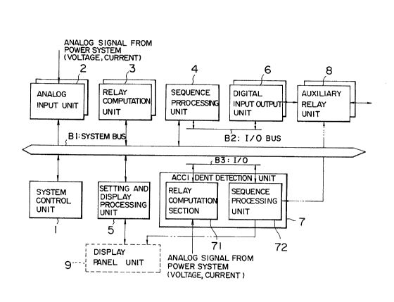
; 10 These units are a system control unit 1 for a multi-
processor system, an analog input unit 2 for A/D
conversion of an analog input and processing through
a digital filter, a relay processing unit 3, a sequence
processing unit 4, a setting and display processing
unit 5, a digital input/output unit 6, an accident
detection unit 7, an auxiliary relay unit 8 and a
display panel unit 9.
, .~
The units 1 to 5 are connected to each other
through a general-purpose bus Bl. The sequence proces-
sing unit 4 and the digital input/output unit 6 areconnected by an input and output I/O bus B2 different
from the general-purpose bus Bl.
Further, a sequence processing section 72 and
a relay computation section 71 in the accident detection
unit 7 are connected by an I/O (input/output) bus B3
different from the buses Bl and B2.
The system also comprises a power unit not
shown for driving the units.
- 21 -
2 ~ 7 ~
1 Now, explanation will be made about an example
of the data transfer control between the units 1 to 5
connected to the general-purpose system bus Bl, that
is, the data transfer control of a multiprocessor with
reference to Figs. 2 and 3. In Fig. 2, the units 1 to
5 are identical to those designated by the same reference
numerals in Fig. 1.
In the system control unit 1, numeral 10
designates a control section including a general-purpose
microprocessor, numeral 11 a direct memory access
controller (DMAC) for high-speed data transfer, and
numeral 12 a data memory.
In the analog input unit 2, numeral 20
designates a signal processing section including a
digital signal processor DSP of floating point arithmetic
type (which may be replaced by a fixed point arithmetic
type with equal effect), and numeral 21 a dual-port
data memory including a dual-port random access data
memory (DPRAM).
In the relay processing unit 3, numeral 30
. designates a computation processing section including
a DSP of floating point arithmetic type (which may be
replaced with equal effect by a fixed point arithmetic
type), and numeral 31 a dual-port data memory including
~ 25 a dual-port random access data memory (DPRAM).
`~ In the sequence processing unit 4, numeral
40 designates a sequence processing section 40
including a general-purpose microprocessor and numeral
- 22 -
-: 2 ~ 7 ~
1 41 a dual-port data memory including a DPRAM.
In the setting and indication processing unit
5, numeral 50 designates a setting and display processing
section including a general-purpose microprocessor,
and numeral 51 a dual-port data memory including a
DPRAM.
Also, in Fig. 2, a signal line ~ carries an
, interrupt signal for notifying a data fetch period,
and signal lines a to e fault notification and recogni-
tion signals (SYS FAIL) for each unit.
Now, a data transfer system according to this
embodiment will be explained with reference to Fig. 3
in addition.
~ Fig. 3 illustrates data transfer timings in
- 15 time series. In Fig. 3, (a) designates the processing
of the system control unit 1, (b) the processing of
the analog input unit 2, (c) the processing of the
-~ relay computation unit 3, (d) the processing of the
; sequence processing unit 4, and (e) the processing of
the setting and indication processing unit 5. In this
diagram, the dotted arrows of ~ to ~ indicate the
directions of data transfer.
First, the system control unit 1 providing
a master unit (a unit which obtains the right to use
the general-purpose system bus to start data transfer)
is supplied with an N-period data ~ from the analog
input unit 2 making up a slave unit (a unit responding
~ to the data transfer made by the master unit). This
:
~ - 23 -
2 ~
1 data is a voltage or current data of the power system,
for example, processed throuqh a digital filter in
the N period by the analog input unit 2 using a sample
data in and before the N-l periods. The data ~ may
be input either in the control section 10 or the DMAC
11 of the unit 1. The data Q thus input is stored
in the data memory 12.
The system control unit 1 transfers the data
~~ stored therein as an input to the relay computation
; 10 unit 3 making up a slave unit, which data is designated
by ~ in Fig. 2.
Further, the relay computation result ~
computed in the N period (using an analog input unit
output in and before the N-l period) is applied and
stored in the data memory 12 of the unit 1.
The system control unit 1 then transfers the
data ~ stored therein as an input to the sequence
~!processing unit 4 making up a slave unit, which data
is designated by ~ in Fig. 2.
Further, the sequence processing result ~
computed in the N period (using the relay computation
.
result in and before the N-l period) is
applied and stored in the data memory 12 in the unit 1.
The system control unit 1 then transfers the
'25 data ~ stored therein as an input to the setting
- and display processing unit 5 making up a slave unit,
which data is designates as ~ in Fig. 2.
Furthermore, the relay set value ~ stored
- 24 -
:`:
2 ~ 7 ~
'.',
1 in the DPRAM of the unit 5 is applied as an input, and
stored in the data memory 12 of the system control unit
1. This data ~ , which is a set value for the relay,
is incorporated into the data ~ and transferred by
the system control unit 1, together with the data ~
applied from the unit 2, to the relay computation unit
3 at each sampling time, and is stored in the DPRAM of
the unit 3. By so doing, a change in the set value is
.,~
met immediately.
As obvious from Fig. 3, it is understood that
upon completion of data transfer, each unit is capable
of fully processing the assigned functions before the
next sampling time. Specifically, from the completion
~ of data transfer at a particular timing, each unit is
`~ 15 in a position to make computation making full use of
the sampling period with the data for particular timing.
This is due to the provision of the dual-port data
memories 21, 31, 41 and 51 in the units shown in Fig. 2.
The data transfer timing ~ in Fig. 3 is
effected by an interrupt signal line ~ shown in Fig. 2.
This signal line ~ is synchronous with a sample command
for sampling the voltage and current of the power system
` and is issued from the unit 2. This timing is identical
to the sampling period of the original sampling signal
~` 25 frequency-divided appropriately.
The data transfers ~ to ~ are of course
; effected following the transfer ~ as easily
understood.
;' .
- 25 -
`'
.
20~7~
1 The foregoing description concerns the
division of the functions of a digital protective relay
system applied to the present embodiment, a general
- block configuration and examples of data transfer
between the divided units.
In the aforementioned embodiment, the system
control unit 1 controls the other four units 2 to 5.
The units controllable by the system control unit 1,
however, are not limited to them. Other units to be
controlled may be added to the extent that the transfer
processing to all the units is covered within a single
processing cycle of the system control unit 1 as shown
- in Fig. 3.
` For addition of a unit, the unit may be
connected to the system bus Bl and an address is set
for the particular unit while at the same time modifying
the control program of the system control unit.
A unit of the same function as a given unit
may be added if the object of addition is to improve
;~ 20 the processing capacity of the given unit. If it is
desired to add a different function to the system, on
the other hand, a unit having such a function may be
- added.
By adding an analog input unit, for example,
more signals are processable. If a relay computation
unit is added, on the other hand, more computations are
- made possible, thus attaining multiple functions and
high performance of the relay.
- 26 -
'';
. . .
.~ ' .
20~7~
; 1 By adding a unit having a different function,
by contrast, various functions may be added to the
digital relay. If a communication function is provided,
for instance, information exchange with other relay
systems is made possible, or central control is attained
at a master unit with the system as a slave unit.
It is of course possible in this system not
only to add units but also delete or modify any of
the units.
For example, the computation unit may be
replaced by a unit capable of operation at higher speed.
In this way, the processing capacity within a period is
- improved for an increased volume of processable
information. As a result, more signals become pro-
cessable. Also, the computation that has thus far been
executed by a plurality of computation units becomes
- processable by a fewer number of units, thus decreasing
the number of units required. As long as the information
to be processed is identical to each other, in
-~ 20 contrast, the computation of high accuracy or complicated
~ in nature may be executed in a limited time, and there-
- fore the system accuracy and functions are improved.
This principle is applicable to system
- construction, and various systems including a digital
relay system may be built up by selecting the units
according to the object.
In this way, according to the method of the
present embodiment, various systems are built up to
'
- 27 -
- " 2 ~ 7 ~L `
.
;~ 1 meet the particular object, and the system thus built
up is so flexible that it is easily expanded, has
functions added thereto, improved in speed or accuracy
or functions.
Now, an outline of a digital protective system
for power applications will be explained prior to
detailed explanation of the respective units. The
. processing operation in general will be explained with
reference to Figs. 4, 5, 6A and 6B. First, the general
,. .
processing operation of a power protective system will
be explained with reference to Fig. 4.
Step 2001 is supplied with information from
a power system that is the voltage and current of a
transmission line, for example, and converts an analog
amount into a digital one.
Step 2002 detects an electrical amount for
accident detection or control. The electrical amount
thus detected includes the magnitude of voltage or
current at the time of an accident of the power system,
the impedance Z up to the accident point, resistance
component R, reactance component X, direction of the
. accident point or frequency at the time of accident.
Step 2003 compares the electrical amount
detected at step 2002 with a predetermined set value.
, 25 If the comparison shows an accident, the process
proceeds to step 2004.
Step 2004 decides whether the accident
condition determined at step 2003 is sustained, and if
,~
- 28 -
:~ 20~7~
1 sustained, the process proceeds to step 2005.
Step 2005 stores the information related to
the accident decided in the preceding steps.
Step 2006 effects a well-known system sequence
processing (which may be combined with an external
condition or timer) on the basis of the various relay
operations stored in step 2005. If an accident is
decided, a cut-off command is issued to the circuit
breaker.
10Step 2007 checks and monitors the system.
The digital control protective system for
power applications is for executing the above-mentioned
` processing operation within the sampling period of the
analog input repeatedly for each sample.
15Fig. 5 shows an example of a reactance relay
; (for one element) and the characteristic of a mho
relay. In Fig. 5, the character jx designates an
inductive reactance component of the impedance.
Step 2002 in Fig. 4 processes about 30 to 50
- 20 relay elements. The sequence processing at step 2006
is made in correspondence with the system on the basis
of these relay element outputs. Set values are shown
by Zl and Z2 in Fig. 5, which values determine a protec-
- tion range in the case of a protective relay. These
values are changed on line by the human from outside
the system in the case where the power system or the
associated protection range is changed, as is well known.
Fig. 6a shows an example of the processing
- 29 -
: 2~a57~
1 flow of a reactance relay shown in Fig. 5 and Fig. 6B
shows example of waveforms in which the steps Sl to S7
correspond to the steps Sl to S7 in Fig. 6A.
In the case of this reactance relay, first,
the voltage and current data are applied (steps 1 and 2),
~ various computations are made about these inputs (steps
- S3 to S7), and the computation result is compared with
a set value (step S8). If the computation result is
larger than the set value, a counter (not shown) for
checking the sustaining time of a fault is incremented
by +l (step 9).
Then, step S10 checks whether the count on
the counter has exceeded a predetermined value. If the
count is larger than the predetermined value, it is
decided that the condition is prevailing for energizing
the relay, and an "1" output is produced at the element
relay (step Sll). If the count has not yet reached the
predetermined value, by contrast, a "0" output of the
element relay is produced while leaving the relay off
(step S12).
In the case where step S8 finds that the
computation result is smaller than a set value, the
counter is cleared (step S13), so that the output of
the element relay is of course zero (step S14).
An outline of the power protective relay
system will be understood from the foregoing explanation.
Now, explanation will be made about a
configuration and the processing functions of each unit
. ,
- 30 -
-: 2 ~ 7 ~
1 shown in Fig. 1 embodying the present invention in
which the functions of a power-system digital protection
system are optimally distributed to meet the require-
ments of compactness, system expansion and multiple and
higher functions while at the same time realizing a
high performance (accuracy and speed) and high
reliability.
First, a configuration and an outline of
processing operation of the analog input unit shown in
Fig. 1 according to an embodiment of the present inven-
tion will be explained with reference to Figs. 7 and 8.
A configuration of the analog input unit 2 (in Fig. 1)
:~-
is shown in Fig. 7.
In Fig. 7, numeral 201 designates a filter for
-~ 15 preventing an aliasing error of a plurality of chennels,
numeral 202 a sample hold circuit (S/~) for a plurality
of channels (all-channel simultaneous sampling system),
numeral 203 a multiplexer (MPX), numeral 204 an
analogjdigital converter circuit, numeral 205 a dual-
port buffer memory using a dual port random access
memory (hereinafter called DPRAM), numeral 206 a timing
generation circuit, and numeral 207 an interface circuit
for synchronizing the units or a particular unit with
other systems or the like (such as an input signal).
- 25 Numeral 200 designates a digital signal
processor (hereinafter called DSP), numeral 208 a program
memory of the DSP 200, numeral 209 â dual-port data
memory using the DPRAM, numeral 210 a system bus
- 31 -
20~7~
1 interface circuit, numeral 211 an interrupt generation
circuit, and numeral 212 a fault detection circuit.
: A signal line ~ is for carrying an interrupt
generation signal (for the unit 1) to take in the data,
and a signal line e for carrying a fault notification
and recognition signal (SYS FAIL~.
The buffer memory 205, the DSP 200, the program
memory 208, the dual-port data memory 209, the inter-
rupt generation circuit 211 and the fault detection
~ 10 circuit 212 are connected to the local bus LB. Also,
- the interrupt generation circuit 211 and the fault
detection circuit 212 are connected to the system bus
sl. Further, the dual-port data memory 209 is connected
: to the system bus Bl through the system bus interface
circuit 210.
Now, an outline of the processing operation
:
will be explained with reference to Fig. 8.
; After the initialization at step 2020, step
: 2021 checks whether a data input interrupt has occurred
after A/D conversion of input information (system
voltage and current) by checking the signal line X. This
is effected by the DSP 200 shown in Fig. 7.
In the case where a data input interrupt has
occurred, the data of all the channels for the particular
sampling time is applied at step 2022, and step 2023,
using the particular data and other data stored at a
previous sampling time as required, effects the filter
- computation (digital filter computation) for all the
~ r~
2 ~ e3 7 11
1 the channels. This computation is of course executed
by DSP 200 in compliance with a command stored in the
program memory 208. An outline of the DSP and the
digital filter computation will be explained later
herein.
Step 2024 monitors and checks for improving
the reliability. This monitoring and checking operation
-. will be described later herein.
~; Step 2025 operates the counter C stepwise,
and step 2026 decides whether the counter C has reached
` ~ a predetermined value (~). The operation of steps 2025
and 2026 is performed by counting the number of data
input interruptions at step 2021. This counter C is
set, for example, in the DSP 200.
In the case where step 2026 decides that a
predetermined value has been reached, step 2027 clears
the counter. Step 2028 stores the result of filter
~- computation for all the channels in the dual-port data
~ memory (DPRAM) 209, followed by step 2029 for initiating
":'.
:~ 20 an interruption to fetch the data against the system
control unit 1 in Fig. 1.
As seen from the foregoing description, the
analog input unit 2 according to the present embodiment
is different in the processing sequence from the analog
input for the digital realy described in the Journal
of the Institute of Electrical Engineers of Japan,
Vol. 105, No. 12 described above.
,,
Specifically, the latter well-known analog
20~57~
.
~; 1 input is effected from a filter (analog) to a S/H
(sample hold) to MPX (multiplexer) to A/D (analog/digital
conversion) to predetermined computation. In contrast,
the analog input section according to the embodiment
under consideration is effected from a S/H (sample
hold) to A/D to digital filter to a predetermined
computation.
Also, as clear from step 2026 in the processing
flow of Fig. 8, the period of digital filter computation
at step 2023 is 1/~ Positive integer) of the period
for data transfer to another unit. Assume that the
- computation period of the digital filter is 167 ~s
(6-kHz sampling) and ~ is 10, for example. The period
of data transfer to another unit (the system control
unit 1 shown in Fig. 1 according to the present
embodiment) is 1667 ~s (equivalent to 600-Hz sampling).
Specifically, the digital computation is effected in a
period 1/10 the period of digital protective computation.
The value of ~ may of course be set or changed as
desired according to the system involved.
If a multiplicity of channels are required
by a system, on the other hand, a plurality of analog
input units may of course be connected to a plurality
of system buses respectively, and these units are
synchronized through the interface circuit 207 shown
in Fig. 7 for parallel processing.
- As will be seen from the foregoing descrip-
tion, the analog input unit according to this embodiment
- 34 -
2 ~ 7 ~
1 is such that the errors of S/H, MPX and A/D (offset
voltage, noise, quantization errors) are collectively
removed by the digital filter and the resulting data is
used for an intended relay computation, thus greatly
improving the characteristics as compared with the
conventional configurations.
Now, an embodiment of the system control unit
1 shown in Fig. 1 will be explained with reference to
Fig. 9.
In Fig. 9, numeral 100 designates a general-
purpose microprocessor, and numeral 101 a direct memory
- access controller (hereinafter called DMAC) for high-
speed data transfer.
; Numeral 102 designates a program memory using
a PROM, for example, numeral 103 a data memory using a
RAM, numeral 104 a set data memory for storing set data
including settings, constants and coefficients by use
of an electrically erasable and rewritable nonvolatile
memory E PROM, and numeral 105 an analysis data memory
including a static random access memory (SRAM) and
a nonvolatile memory E PROM similar to the above-
mentioned memory packaged in the same chip (IC) for
storing data at high speed and analyzing a fault which
may occur.
Further, numeral 106 designates a system
logic including a system reset, system clock and a bus
access reconciliation circuit, numeral 107 a system
interruption decision circuit, numeral 108 a fault
- 35 -
- ~ ~ ~
2 ~ 7 ~
1 detection circuit, numeral 109 a communication interface
(RS-232C) circuit for connecting with a personal
computer or the like, and numeral 110 a system bus
; interface circuit.
The analysis data memory 105, as described
above, includes a SRAM and an E PROM and has such a
function that all the data in the SRAM are transferred
to the E PROM at a time by a store control signal
(pulse) on the one hand, and all the data in E2PROM
to SRAM at a time by a recall control signal (pulse)
;.~ on the other.
As a result, if the system is so configured
that a store control signal is generated on the occasion
of power failure or upon detection of a unit fault
or the like, the immediately preceding data are
maintained in the nonvolatile E2PROM suitably for
; restarting the operation or analyzing the fault.
The microprocessor 100 is connected to a
local bus LB. The local bus Ls is connected with a
~: 20 DMAC 101, a set data memory 104, an analysis data
- memory 105, a system interface circuit 110, a program
memory 102, a data memory 103, a fault detection circuit
108, a communication interface circuit 109 and a system
interrupt decision circuit 107.
Now, explanation will be made about a configu-
ration of the relay computation unit 3 shown in Fig. 1
according to an embodiment of the present invention
with reference to Fig. 10.
::
- 36 -
2 ~ 7 ~
,
1 In Fig. 10, numeral 300 designates a processor
(DSP) for computation processing, numeral 301 a DSP
program memory using an EPROM, numeral 302 a dual-port
data memory using a data storage DPRAM, numeral 303
a system bus interface circuit, and numeral 304 a fault
detection circuit. An outline of the DSP will be
explained later herein.
This relay computation unit is for processing
the steps 1 to 5 at high speed. Specifically, it is a
processor unit for processing the operation for the
digital control and protection of a power system.
Depending on the particular system, a plurality of
these units may be connected to a system bus for
- parallel processing.
The processing operation according to an
embodiment of the system control unit 1 shown in Fig. 9
will be briefly explained with reference to Fig. llA.
An outline of the processing operation of the relay
computation unit 3 in Fig. 10 is also shown in Fig. llB.
The processing operation of the system
control unit 1 is effected in the manner shown in Fig.
- llA.
(1) After initialization, decision ~waiting for
interrupt) is made as to whether there is a data intake
request (~ times the digital filter computation period)
from the analog input unit 2 (steps 1000, 1001).
(2) As explained with reference to Figs. 2 and 3,
data transfer is made between the units (step 1002).
Specifically, data transfer control between the units is
- 37 -
2 ~ 7 1
1 effected by the system control unit 1.
(3) Mutual checking is made to see whether data
transfer is normally made between the units (steps 1003
to 1007).
- 5 (4) The local and system interrupt processing is
~ effected (steps 1008, 1009).
i (5) The data to be stored in the set data memory
104 and the analysis data memory 105 shown in Fig. 9 are
compiled. At the same time, the data is saved in case
a fault occurs in the system (steps 1010 to 1012).
(6) Self diagnosis (self check) is effected (steps
1013, 1015).
The system control unit 1 repeatedly executes
- the above-mentioned processings each time of a data
intake request, that is, in each protection (control)
computation period. It will be easily inferred that
in the case of exchange or addition of units, the data
transfer control corresponding thereto is of course
changed for executing the processing. Though not shown,
the hardware and software for controlling these
operations are of course built in the units.
Now, an outline of the processing operation of
- the relay computation unit 3 shown in Fig. 10 will be
explained with reference to Fig. llB.
(a) After an initialization step, decision is
made as to whether data transfer from the system control
unit 1 has been finished (waiting for an interruption
using the signal line INTRY in Fig. 10) (steps 3000,
:,
: '~
- 38 -
, .
2~0~7~
1 3001).
(b) The data transferred to the dual-port data
memory in Fig. 10 is transferred again to the data
~ memory in the DSP 300. This is for processing the
computation using the DSP 300 at high speed.
(c) The protective relay processing operation
for the power system according to a predetermined
algorithm is effected (step 3003).
(d) The computation result is transferred to the
dual-port data memory 302 shown in Fig. 10 (step 3004).
This computation result is transferred again by the
system control unit 1 to the sequence processing unit
4 described later herein.
(e) The constant monitoring operation (steps
3009 to 3011) including mutual check and self check
is effected to see whether data transfer with the
system control unit 1 is normally effected (steps 3005
to 3009).
- As explained above, the relay computation unit
3 is operated repeatedly for each data transfer period,
that is, for each computation period. The computation
time can be fully used without overhead from an
interrupt for end of data transfer to the next transfer
interrupt, thus improving the processing capacity.
Also, the relay computation processing of step 3003 is
for executing a multiplicity of types and numbers of
processing operations mentioned in Figs. 5 and 6.
Now, an example of the technique for detecting
- 39 -
~,
,,.. .. -:.. :-.. :, ... . .... ;
2 ~ 71
1 a fault by mutual check and monitor by data transfer
between the units (system control unit 1 and the relay
computation unit 3) will be explained with reference
to Figs. llA and lls.
First, the monitor operation of the system
control unit 1 shown in Fig. llA will be explained.
(Step 1003)
This step is for checking to see whether the
relay computation unit 3 has transferred thereto a
predetermined data (A in this example) in every period
from the system control unit 1. The system control
unit 1 transfers a fixed data A in every period to a
given fixed area (say, address N) of the dual-port data
memory 302 in Fig. 10.
(Step 1004)
This step is for the system control unit 1 to
take in a fixed data B from a given fixed area (say,
address M) of the dual-port data memory 302 in Fig. 10.
The data B at address M is cleared in every period by the
:.
` 20 system control unit 1 and set by the relay computation
~-; unit 3 in every period.
(Step 1005)
In view of the fact that step 1004 receives
the data (normally, B) from address M of the dual-port
- 25 data memory 302 in Fig. 10, the data B should be stored
at address M in the next period if the relay computation
. unit 3 is normal. Step 1005 is for clearing the data B
` to discriminate the case where the data remains stored.
- 40 -
, ~ -., ~, . ,
"
, . .
` ~ 2~
1 (Step 1006)
This step is for deciding whether the data
applied from address M is B or not. If it is B, it is
decided that data transfer with the relay computation
unit 3 is also normal. Further, if the data is B,
it is decided that the relay computation unit 3
- processes the step 3005 in Fig. llB normally. In the
case where the data received from address M is not B,
it is decided that the relay computation unit 3 is not
operating normally. This is because whether a data
transfer is normal or not is easily decided by making
access to another address (say, address M+l) if the
address M is not accessible normally.
Now, the check and monitor operation of the
relay computation in Fig. 11 B will be explained.
(Step 3005)
This step is for storing a fixed value B in
every period at address N of the dual-port data memory
302 in Fig. 10. This is effected by the system control
unit 1 taking in a fixed value in every period to decide
whether the relay computation unit 3 is operating in
normal way. Specifically, this step is one for having
other units monitor the particular unit.
(Steps 3006, 3007, 3008)
- 25 These steps enable the relay computation
unit 3 to monitor the system control unit 1.
Step 3006 takes in data from address M of the
dual-port data memory 302 in Fig. 10. As mentioned
- 41 -
'3,~
:;
2~571
1 above, the fixed value A is transferred in every period
to this address M if the system control unit 1 is
normally operating.
Step 3007 is for clearing the data at address
M received at step 3006. If the system control unit 1
is normally operating, the fixed value A should be
transferred to address M again before the next period.
Step 3008 is for deciding whether the data
received from address M is A or not. If it is A, it
is decided that the system control unit 1 is normal,
and if the data is not A, it is decided that the system
control unit is faulty.
- Instead, the memory including address M may
be faulty when the decision is that the data is not A.
Whether the memory is faulty or not may be decided,
however, by making access by the DSP 300 of the relay
computation unit 3. If the decision is not the data A,
on the other hand, the system bus interface circuit 303,
~` not the system control unit 1, may be faulty in Fig. 10.
This discrimination, however, is made from the fact
that if the system bus interface circuit 303 is faulty,
the processing operation (access to address N) of the
system control unit 1 should also be faulty).
It will be understood from the foregoing
description that the processors mounted on both the units
1 and 3 make mutual check possible. As a result, a
fault of each unit is detectable both quickly and
- easily.
.,~
- 42 -
20~0~7~
1 The system control unit 1 also makes mutual
check with other units in quite the same manner as
above. (Step 1007 in Fig. llA)
Now, a configuration of an embodiment of the
sequence processing unit will be explained with refer-
ence to Fig. 12.
In Fig. 12, numeral 400 designates a sequence
processor for effecting the sequence processing opera-
tion by use of a general-purpose computer in a power
protective relay system, numeral 401 a program memory
using a PROM storing a sequence processing program,
numeral 402 a data memory (RAM), numeral 403 a dual-
port data memory using a DPRAM, numeral 404 a system
bus interface circuit, numeral 405 an input/output bus
(hereinafter called the I/O bus) for taking interface
with the digital input/output unit 6 (in Fig. 1)
described later herein, numeral 406 a fault detection
~ circuit, and numeral 407 a general-purpose communication
- interface circuit (such as a general-purpose RS-232C)
for taking interface with a personal computer or the
like.
A configuration of an embodiment of the digital
input/output unit 6 connected to the sequence unit
mentioned above through the I/O bus wlll be explained
with reference to Fig. 13.
;~ In Fig. 13, numeral 600 designates an I/O bus
interface circuit, numeral 601 a data latch circuit,
; numeral 602 a photocoupler, numeral 603 an output
- 43 -
2 ~ 7 ~
1 buffer circuit, numeral 604 an input buffer circuit,
- and numeral 605 a photocoupler. The photocouplers
602 and 605 are both interfaces for electrical insula-
tion.
Now, the processing operation of the sequence
processing unit 4 described above will be briefly
explained with reference to Fig. 14.
(1) As in the relay computation unit 3, after
initialization (step 4000), it is decided (step 4001)
whether all the data transfer necessary for sequence
processing from the system control unit 1 has been
finished or not. This decision is made by checking an
interrupt signal INTSEQ generated upon completion of
data transfer from the system control unit 1 as shown
in Fig. 12.
: ,.
(2) The data transferred from the system control
unit 1 to the dual-port data memory 403 shown in Fig. 12
- is further transferred to the data memory 402 (step
- 4002).
(3) Digital input processing is effected through
the I/O bus 2 (step 4003).
(4) The sequence processing is effected in
accordance with a predetermined algorithm (step 4004).
(5) The check and monitor processing in the
respective units, and mutual check and monitor processing
-:
between the units similar to the one described for
the system control unit 1 and the relay computation
unit 3 are executed (steps 4005 and 4006).
- 44 -
- 2 ~ 7 ~
1 (6) The result of sequence processing is supplied
as an output (digital output) through the I/O bus B2
(step 4007). This output is applied to the digital
output section in Fig. 13 through the digital output
section in Fig. 13. This information of course contains
a cut-off command for an intended circuit breaker.
(7) Further, the result of sequence processing
stored in the data memory 402 in Fig. 12 is transferred
(step 4008). This is a process for enabling the system
control unit 1 to make access to this data. The system
control unit 1 transfers this data to the setting and
indication processing unit 5 described later herein.
A configuration and an outline of processing
operation of the setting and indication processing unit
5 will be explained with reference to Figs. 15 and 16.
Fig. 15 shows a configuration of the setting and
indication processing unit 5.
In Fig. 15, numeral 500 designates a micro-
processor, numeral 501 a program memory (PROM), numeral
502 a data memory (RAM), numeral 503 a dual-port data
memory (DPRAM), numeral 504 a system bus interface
'~ circuit, numeral 505 a set value memory including a
nonvolatile memory E PROM for storing a set value,
~ numeral 506 a fault detection circuit, numeral 507 a
-~ 25 communication interface circuit with a personal computer
or the like, and numeral 508 a panel interface circuit
with the display panel 9 (in Fig. 1).
The processing operation of this setting and
- 45 -
2 ~ 7 ~
1 display processing unit 5 will now be briefly explained
with reference to Fig. 16.
(1) In exactly the same manner as the sequence
processing unit 4, after initialization (step 5000~,
` 5 it is decided whether all the data transfex from the
system control unit 1 has been completed (step 5001).
(2) The display processing on the display panel
9 in Fig. 1 is effected (step 5003).
(3) The processing is effected for changing the
set value (coefficient) from the display panel 9 in
~ Fig. 1 (steps 5004 and 5005).
(4) The checking and monitoring in the units
and mutual checking and monitoring between the units
are effected in exactly the same manner as in the
sequence processing unit 4 mentioned above (step 5006).
(5) The coefficient (set value) stored in the
, set value memory 505 in Fig. 15 is transferred to the
dual-port data memory 503 (step 5007). This is a
process for enabling the system control unit 1 to
transfer the set value therefrom to other units (such
;'.
~ as the relay computation unit).
From the foregoing description, the configura-
tion and the general processing operation of the setting
and display processing unit 5 will be understood.
Finally, the functions and the general
processing operation of the accident detection unit 7
shown in Fig. 1 will be explained.
The unit 7 is separated from the other units
- 46 -
2 ~ 7 ~ ~`
1 described above in consideration of system reliability.
Specifically, it is not electrically connected in both
input and output with any of the units explained above.
The accident detection unit performs the same
processing operation as any combination of units
mentioned above. As a result, as shown in Fig. 1,
information from a power system is received, and the
input thus received is processed in accordance with a
predetermined algorithm, so that the result of processing
is applied to the auxiliary relay unit 8 shown in Fig. 1
as in the aforementioned cases. Specifically, the
accident detection unit 7 is for fail-safe applications.
The scale of the processing operation performed by this
unit is generally considerably smaller than in any
combinations of units mentioned above.
configuration and the processing operation
of this unit will be briefly explained below.
(1) In Fig. 1, numeral 71 designates a relay
' computation section of the accident detection unit 7,
which is configured in the same way as the analog input
unit 2 shown in Fig. 1. The following processing
operations are effected:
The analog input A/D converted and processed
in a digital filter
~ Set value received as an input (from the part
- 72 described later herein)
Relay computation for accident detection
Diagnosis
,
- 47 -
'
,
2 ~ 7 1 ~ "
:
1 (2) In Eig. 1, numeral 72 designates a sequence
processing section of the accident detection unit 7,
as the processing operation thereof is briefly described
below.
(a) The computation result of the accident detection
relay computation section 71 is received through the
I/O bus (B3) in Fig. 1 and digital input and output
, processing thereof.
(b) Sequence processing for accident detection
relay
:,
(c) Setting and display processing for accident
detection relay
(d) Diagnosis
This sequence processing section 72, as will
'~ 15 be easily understood, has the same hardware configura-
` tion as the sequence unit 4 in Fig. 1 with the digital
input and output unit 6 and the display panel interface
` circuit packaged therein.
Each unit according to the foregoing embodi-
^ 20 ments is configured of circuit elements such as ICs
mounted on a printed board. In this case, an IC or
the like may be selected for each unit separately,
- but may be more desirably shared among the units. An
embodiment of such a configuration will be explained
below.
- In the embodiment shown in Fig. 1, the
following component elements, for example, may be
shared by the analog input unit 2 and the relay
- 48 -
:,
2 ~
,
1 computation unit 3.
la. DSP
lb. DSP program memory (PROM)
lc. Dual-port data memory (DPRAM)
ld. System bus interface circuit
le. Fault detection circuit
lf. Local bus
Also, in the embodiment of Fig. 1, the system
control unit 1, the sequence processing unit 4 and the
setting and display processing unit 5 may share the
following component elements:
2a. General-purpose microprocessor
; 2b. Program memory (PROM)
; 2c. Data memory
2d. System bus interface circuit
2e. Fault detection circuit
~' 2f. Communication interface circuit
2g. Local bus
Further, the units 1 to 5 may share the
, ;
, 20 following component elements:
. . .
3a. Program memory (PROM)
3b. System bus interface circuit
..~.
- 3c. Fault detection circuit
~ 3d. Local bus
-, 25 The aforementioned sharing is illustrative
and possible in various forms taking the capacity,
^ packaging conveniences, etc. of each element into
consideration. The component elements to be shared
,"'
- 49 -
2~ 37~
1 among different units are mounted on a common printed
board to which component parts not shared are added to
make ùp each unit. As a result, it is necessary to lay
out a printed board with a space for mounting common
-~ 5 component elements and also one for carrying non-common
component elements.
Further, this concept may be advanced a step
further, and component elements that can be shared are
appropriately combined into an LSI.
:~ 10 In sharing component elements, if component
elements not required for a given unit are also mounted
. .,
thereon, the sharing of component elements is enhanced,
so that by writing a specific program into each program
memory, it is possible to configure systems having the
same hardware configuration but different functions.
. This is very preferable for system standardization and
; unification.
An example of the hardware configuration
containing common component elements o the units will
be explained below.
A general-purpose microprocessor, a PROM, a
DPRAM, a RAM, a system bus interface circuit, a fault
detection circuit, a communication interface circuit and
a local bus make up a hardware configuration common to
a plurality of units on a single printed board.
Also, a DSP, a DPRAM, a PROM, a system bus
interface circuit, a fault detection circuit and a
local bus makes up a hardware configuration common to
'
-- 50 --
2 ~ 7 ~
1 a plurality of units on a single printed board.
Each device used in the hardware configurations
according to this embodiment is only an example, and
other devices which can realize the same function may
be used alternatively. For example, a dynamic RAM may
be replaced with a static RAM or a PROM with an EPROM.
Also, the processor may replaced with one higher in
. ~.
speed or larger in processing capacity. In the case
where the signal amount to be processed is small, on
: - 10 the other hand, a device lower in performance but low
in cost may be used in place.
In such a case, the whole system is not
. affected as long as there is no change in the function
or performance of an input or output as related the
system bus of each unit. As a result, free designing
for each unit is possible on the one hand and design
change is facilitated on the other.
Specifically, according to the present embodi-
-~ ment, each unit may be built in the system to the extent
that data input into and output from the system control
unit according to a predetermined specification is
~-~ possible. According to the present embodiment, there-
fore, units having various functions may be incorporated
; in the system freely, and also even after a system is
; 25 built up, the units may be improved, modified or
increased in number as required.
Now, the DSP (digital signal processor) making
up a key component of a configuration embodying the
-- 51 --
.,~
- 2 ~ 7 ~
1 present invention will be explained.
A detailed configuration of an embodiment of
` the DSP is shown in Fig. 17.
; The DSP according to this embodiment, as
! j 5 shown, includes an address register 222 for designating
an address in an external memory, a data register 223
used as a parallel port, a data RAM 224, a high-speed
parallel multiplier 225 of _ bits x _ bits, an
:
- instruction ROM 226, an arithmetic logic unit ALU 227
for performing such calculations as addition and
subtraction, a register 228 such as an accumulator,
a control circuit 229 for controlling the interrupt
or the like of a control signal (a, b or c) with an
external circuit, and an internal bus 230 of the DSP.
The multiplier 225 is for multiplying the
contents of the input signals A and B during one
instruction cycle and applying the result C thereof
to the internal bus 230.
The ALU 227 is to add or subtract the data
, 20 derived from the internal bus 230 and the register 228
- to or from each other and writes the result thereof
in the register 228.
The DSP has a feature in that, as well known,
the-sum-of-products computation is possible during one
instruction cycle and that the pipeline processing is
available thereby to realize a high-speed numerical
computation of fixed and floating point data. As a
result, the input data relating to multiple input
. - 52 -
20~a~37)L
,~ '
1 points may be processed through a filter in real time.
This concept is not applicable to a general-purpose
`~ microprocessor low in processing speed.
An embodiment of the digital filter using a
. ~
: 5 DSP will be explained.
- Figs. 18A and 18B are diagrams schematically
showing typical block configurations of a digital
~; filter. Fig. 18A shows an IIR (infinite-extent impulse
response) type of filter, and Fig. 18B shows a FIR
(finite-extent impulse response) type of filter.
~- In Fig. 18A, Xn designates an input signal
sign, numeral 241 a coefficient block, K a gain
~ 1~ A2~ Bl and B2 filter coefficients
Numeral 242 designates delay blocks including a one-
period delay block (Wn-l) for delaying the signal Wn
by a one unit-time corresponding to one period T, and
a block (Wn-2) for delaying the same signal by two
unit-times. Numeral 243 designates an add block, and
Yn a filter output data.
As seen from Fig. 18A, various filters
indicated by equations (5), (6), (7), (8) and (9) below
are realized by regulating the filter coefficient in the
. ,
; shown configuration. H(z) designates a transfer
function, and Z is equivalent to S of an analog system.
(Low-pass filter)
H(z) 1 Bl B2 (l+Z 1)
l-Bl-Z +B2-Z
- 53 -
20t 0~7~
. .` ;
s 1 (sand-pass filter)
H(z) = 2 , -2 ..... (6)
l-Bl~Z + B2-Z
(High-pass filter)
H(z) = ~ 1 Bl Z-l + B2 z-2
...... (7)
(Notch filter)
~(Z) = 2 ~2 . 1 - r-Z 1 + z 2 .......... (8)
1 - Bl Z + B2-Z
where r = 2 cos2~fO T, T is a sampling period, and fO
a blocking frequency.
(All-pass filter)
z-2 _ Bl Z 1 +s2 ....- (9)
; 1 - Bl-z 1 + g2.z-2
In Fig. 18B, X'n designates an input data,
and Y'n an output data. Numeral 244 designates delay
blocks, of which X'n-l is one for delaying one unit-time
and X'n-2 for delaying two unit-times. Numeral 245
,designates a filter coefficient block for setting the
filter coefficients A~o~ A'l and A'2. Numeral 246
designates an add block.
This diagram may be expressed by a computation
formula shown in equation (10) below.
':'
- 54 -
2 ~ 7 1
:
.
n A 0 X n + A l X n-l + A'2 X'n-2
'.` ..... (10)
1 As described above, an input signal is
filtered by digital filter means using a DSP according
` to the present embodiment. This operation is performed
repeatedly for each sampling period T on the basis of a
filter coefficient set in advance. As a consequence,
input signals may be filtered by time division in
software fashion in accordance with the number of input
points, thus meeting the requirements for changing the
:
number of input points, modification of characteristics
.:
and standardization of the printed board.
Also, since the filtering operation is possible
without using an analog filter, this embodiment is
completely free of factors adversely affecting the
elements such as secular or other variations in element
value due to the initial value error or ambient tem-
perature of such devices as resistors and capacitors
unlike in the analog filter, thus assuring a high
accuracy free of adjustment.
Also, an external checking circuit is eliminated
as the need thereof is met by an internal software,
so that the production processes are grealy shortened,
eliminating the need of maintenance, thereby leading
to a higher accuracy, lower cost and other advantages of
,~
the protective relay system.
- 25 Now, an example of an automatic checking
system suitably applied to the analog input section of
- 55 -
2 ~ 7 ~
1 an analog input unit according to the present invention
will be explained.
(Embodiment: Automatic checking ~1))
Fig. 19 is a diagram showing a block configura-
tion of an automatic checking system for the analogsection according to a first embodiment of the present
invention.
In Fig. 19, numerals 201-1 to 201-N designate
low-pass filters (mainly used for prevention of aliasing
errors in sampling and hereinafter abbreviated as LPF)
for removing the high harmonics superimposed on the
input analog signals inl to inN and a digital signal
Tin supplied from an external source while adding these
input signals to each other. Numerals 202-1 to 202-N
designate sample hold circuits (hereinafter called S/H),
numeral 203 a multiplexer (hereinafter called MPX),
numeral 204 an analog-digital converter circuit
(hereinafter called A/D converter), and numeral 205 a
buffer memory for the A/D converted data using a DPRAM.
.~
Numeral 200 designates a DSP (digital signal
processor), numeral 212 a program memory (ROM) for
storing DSP instructions, LB a local bus, numeral 209
a dual-port data memory for receiving data from and
- delivering data to the system bus, numeral 210 a system
bus interface circuit, and Bl a system bus.
Numeral 206 designates a timing generation
circuit for controlling the operation of the S/H
circuits 202-1 to 202-N, the MPX 203, the A/D circuit
- 56 -
201~57~
1 204 and the buffer memory 205 and applying a digital
signal to the LPFs 201-1 to 201-N.
Fig. 20 is a circuit diagram showing in detail
the LPFs 201-1 to 201-N in Fig. 19.
In Fig. 20, numerals 201a, 201b, 201c and
201d designate resistors, numeral 201e a capacitor, and
numeral 201f an operational amplifier (OP amplifier).
The above-described LPFs are for adding an
analog input signal ln and the digital input signal Tin
to each other, and filtering these input signals to
remove the high harmonics.
Now, explanation will be made about the
processing sequence of automatic checking (fault
detection of an analog circuit) of the analog input
~; 15 section according to the present embodiment with refer-
ence to the flowchart of Fig. 21.
(i) Input, combination and A/D conversion of check
signal
The LPFs 201-1 to 201-N in Fig. 19 are supplied
with input signals inl to inN representing the condition
amounts of the power system detected by a transformer,
a current transformer or the like (normally 50 Hz or
60 Hz). Also, they are supplied with a digital signal
(clock signal) of a frequency fn from the timing
generation circuit 206 shown in Fig. 19. The LPFs
201-1 to 201-N function to combine these input signals
while at the same time operating as an anti aliasing
filter for preventing an aliasing error caused by
.~ ,
20~7~
1 sampling.
The filter output is sample-held for every
period T by the S/H circuits 202-1 to 202-N shown in
Fig. 19.
The MPX 203 in Fig. 19 sequentially switches
the outputs of the StH circuits 202-1 to 202-N for
every period T' (period l/n the period: n is an integer)
and applies the data in the S/H circuits to the A/D
conversion circuit 204 shown in Fig. 19. The A/D
conversion circuit 204 converts an analog amount into
a digital amount and stores the result of conversion
into the buffer memory 205 shown in Fig. 19.
These operations are repeated for each period
T, which provides a sampling period of the digital
filter.
(ii) Initialization
As an initialization step, the register and
memory in the DSP 200 and the buffer memory 205 are
cleared to set the initial state (step 2021a). The
processes in and subsequent to (ii) are for energizing
the DSP 200 by a command stored in the program memory
212.
(iii) Data input
Step 2021b transfers the input data stored in
the buffer memory 205 into the DSP 200 through the
local bus LB.
(iv) Filter coefficient input
Step 2021c transfers the filter coefficients
:
- 58 -
~ 20~057~
:
` 1 stored in advance in the program memory 212 into the
DSP 200. These filter coefficients include coefficients
(filter coefficient group A) for passing the frequency
(fO: 50 Hz or 60 Hz) of the power system mentioned
~ 5 above to realize the characteristics for removing high
- harmonics, and coefficients (filter coefficient group s)
for attenuating the frequency fO of the power system
greatly and realizing the characteristics for passing
only the frequency fn of the signal Tin applied from
the timing generation circuit 206. These coefficients
may be supplied through the system bus Bl from other
unlts .
(v) Digital filter computation (1)
Several specific methods of digital filter
. .
computation are available, of which the processing
- operations shown by equations (11~ and (12) are an
~-~ example.
Wn = K~Xn + Bl (Wn-l) + B2 (Wn-2) ..... (11)
Yn = Wn + Al (Wn-l) + A2 (Wn-2) ..... (12)
: ''
; where K: Gain coefficient,
Al, A2, Bl, B2: Filter coefficients
Xn: Input data,
Yn: Output data,
Wn-l: Wn data delayed by one unit-time
Wn-2: Wn data delayed by two unit-times
- 59 -
2 ~ 7 ~
1 The filter coefficient group A is used as
filter coefficients for the filter computation at step
2021d.
Fig. 22A shows an example of the gain-frequency
characteristic of a filter used for the processing
operation at this step. This filter passes the frequency
f0 and attenuates the frequency fn to such an extent as
to have no effect on the protective computation.
The protective computation uses the filter
, 10 output obtained at this step. As a result, the applica-
tion of an input Tin of the frequency fn is of course
free of any effect on the relay characteristic.
: (vi) Digital filter computation ~2)
The filter computation at step 2021e is
exactly the same as that shown in (v) above and the same
computation program is thus involved. The filter
coefficient group B is used as filter coefficients.
Fig. 22B shows the gain-frequency character-
istic of a filter used for the processing operation
performed at this step. Only the frequency component
(fn) of the signal applied from the timing generation
circuit is passed while the other signals are attenuated.
Specifically, the selectivity Q is set to a very high
` level. Also, another computation program may be used
for this step.
(vii) Decision
Step 2021f determines the absolute value of
the filter output for each channel computed at step (vi)
- 60 -
:
2 ~ 7 ~
1 and is compared with a known set value. As a result,
within the range of a known set value, it is decided
that the analog input section, that is, LPFs 201-1
to 201-N, S/H circuits 202-1 to 202-N, MPX 203, A/D
conversion circuit 204 and the buffer memory 205 are
operating in normal way. Outside a known set value range,
on the other hand, it is known that either the analog
input section or the buffer memory 205 is faulty.
According to the present invention, the
aforementioned computation is effected by DSP and there-
fore a computation of very high accuracy is possible,
thus permitting a very accurate decision.
' (viii) Data output
Step 2021g transfers the filter output
processed by the filter at step (v) to the system master
(a unit connected to the system bus and having a system
control function). This process is repeated for each
period T.
The master unit for effecting the aforementioned
control of the system locks a relay on the basis of
the above-mentioned result of decision, while at the
same time preventing a faulty operation by system
fault indication. Also, since it is known that the
analog input unit is faulty, the faulty portion is
localized.
This operation permits high-accuracy and
reliable automatic checking of the analog input section.
Further, the checking of the analog input section which
- 61 -
20~7 ~
1 has thus far been difficult is made possible without
any additional circuit. As a result, all the processes
; from data input to filter computation are effected in
their entirety, thus greatly improving the system
reliability.
In the above-described embodiment, the input
Tin of frequency fn applied to the LPF is explained
with reference to a case where the input is applied
from the timing generation circuit. According to the
present embodiment, the input Tin of LPFs 201-1 to
201-N may be supplied, not from the timing generation
circuit, but as an output of an oscillation circuit
separately inserted with equal effect, as easily
understood.
Fig. 23 shows waveforms produced at various
parts of the embodiment under consideration. (a)
designates an input signal of the power system, (b) a
clock input signal, (c) output waveforms of LPFs 201-1
to 201-N, (d) an output data of the digital filter A,
(e) an output data of the digital filter B, and (f) an
output data determined as an absolute value of the
output data of the digital filter B.
Although the aforementioned embodiment concerns
a case in which the clock signal Tin shown in Fig. 23B
is applied to the LPFs 201-1 to 201-N, not only the
clock signal but also a sinusoidal wave signal or
the like may be applied with equal effect as easily
understood.
- 62 -
20~0~7~
1 (Embodiment: Automatic checking - (2))
Unlike in the above-described embodiment in
which a given clock signal is applied to the LPFs shown
`~ in Fig. 19, the embodiment explained below has a DC
signal applied to the LPFs for automatic checking.
This embodiment has the same circuit configura-
` tion and processing flow as those shown in Figs. 19 and
~ 21.
; Fig. 24A shows exactly the same frequency-gain
10 characteristic as the filter shown in Fig. 22A. Fig.
24B shows the frequency-gain characteristic of a low-
pass filter (a digital filter C using the filter
coefficient group C). As a result, the difference of
this embodiment from the aforementioned ones lies in
15 the filter characteristic of step 2021e (Filter B
replaced by filter C).
Now, the operation of this embodiment will be
explained.
First, one of the two input terminals of the
LPFs 201-1 to 201-N is supplied with an input signal ln
from the power system shown in Fig. 25A, and the other
-~ input terminal thereof with an input signal Tin' making
up a DC voltage of Vref in magnitude shown in Fig. 25B.
S As explained above, the outputs of the LPFs 201-1 to
201-N shown in Fig. 19 take the forms as shown in Fig.
25C.
Specifically, the waveform is such that Vref
is added to the input signal from the power system.
.
- 63 -
,
,
2 ~ 7 ~
1 Now, the DC portion of the filter output to
which the filter coefficient group A is applied is cut
off as shown in Fig. 25D. As a result, the DC portion
of the filter a applied to the protective relay computa-
;5 tion is cut off, and therefore the effect of the
application of a DC signal input that would otherwise
have on the protective relay computation is eliminated
entirely.
Fig. 25E shows an output of the filter C. As
~10 seen from this diagram, if the analog input section
- explained above operates normally, the DC portion
(Vref in magnitude) applied as an input is faithfully
produced as shown in Fig. 25E.
It is, however, easily understood that the
output of the filter C may be multiplied in gain to a
desired degree.
In the case where the analog input section
described above is not operating in normal way, on the
other hand, the output magnitude of the filter C is not
Vref, and therefore a circuit fault is detected earlier
(with a delay only as much as a delay in the transient
response of the filter C), thus greatly improving the
relaibility.
Fig. 26 is a diagram for explaining the embodi-
ment under consideration more in detail. Fig. 26Ashows an output of the filter C, and Fig. 26B a DSP
processing.
Assume that the analog circuit operates
- 64 -
2~ 05711
1 normally before time point Tf, and a circuit fault has
occurred at time point TF.
At time point TF + ~ several samples later,
` the magnitude of the filter output is not Vref. As a
result, a fault of the analog circuit should be capable
of being detected at that time point. Specifically,
a high-speed automatic checking is of course realized.
(Embodiment: Automatic checking - (3))
Still another embodiment will be explained.
This embodiment, like the one explained above, has a
circuit configuration and a computation flow similar to
those shown in Figs. 19 and 21. This embodiment,
- however, is different in the coefficients of the filter
at steps 2021d and 2021e and the input signal Tin applied
to the LPFs 201-1 to 201-N shown in Fig. 19.
Fig. 27A is a diagram showing an example of
the frequency-gain characteristic of a filter used for
passing the frequency fO of the power system and
effecting the protective relay computation.
(The filter coefficient group D is used)
The above-mentioned filter characteristic
is such that the input of frequency fn' is zero.
Fig. 27B is a diagram showing an example of
the gain-frequency characteristic of a filter E (filter
coefficient group E) for cutting off the frequency
component fO of the power system and passing only the
frequency component fn' of the applied signal in
contrast with the case of Fig. 27A.
, .
~ - 65 -
.
:~,~,- - - .-
.,
~ 20~0a71
1 Thus the filter having the characteristic
shown in Fig. 27A which cuts off the input Tin of
frequency fn' has no adverse effect on the protective
relay computation.
Now, the operation of the present embodiment
will be explained.
Fig. 28A shows an S/H signal for sampling
the filter. Fig. 28B is a diagram showing an input
signal Ti' providing an input waveform applied to the
LPFs 201-1 to 201-N shown in Fig. 19.
The S/H signal is synchronized in timing with
the Ti input signal. Specifically, the input signal Ti'
has a period n times (n: Integer) as large as the
period of the S/H signal. Also, the input signal Ti'
has a clock waveform oscillating between positive and
negative sides.
An output waveform of the filter D described
above is shown in Fig. 28C. This filter output assumes
a waveform responsive only to the input signal Ti'
due to the filter characteristic described above, and
under normal operation of the analog input section, is
` identical to the known data at the time points
designated in Fig. 28D. Specifically, since the S/H
signal is in phase with the Ti input signal, the DSP
200 in Fig. 19 is informed of the number of processings
~ it has been engaged from the point of polarity change
- of the input signal Ti', and thus the output thereof
is known in advance. In view of this, if the filter
i
-` - 2 ~ 7
' :
1 output is compared with the known data corresponding
to the sampling time point, a fault of the analog
circuit is discriminated at early time quickly by use
of the DSP.
As a result, a quick fault detection is
possible for every sampling period of the filter, and
therefore the protective relay system can be locked to
prevent a false operation at the time of a fault of
the analog input section.
Also, according to the present embodiment in
which an input oscillated between positive and negative
sides as shown in Fig. 28B, the checking of the A/D
conversion circuit considered very important in the
prior art is also performed, thus eliminating an
additional checking circuit exclusive to the A/D conver-
sion circuit. As a result, the circuit is reduced in
size and improved in reliability.
In respect of the operation flow shown in
Fig. 21, on the other hand, the filter computation for
checking, if limited in computation time, may be effected
in time division but not for every period of filter
.:
computation.
- The aforementioned embodiment for automatic
check of the analog input section eliminates the need
of an additional circuit for automatic check and permits
an accurate fault detection at an early time, thus
improving the reliability as a protective relay system.
Further, even at the time of an accident of
- 67 -
,~
~,
2 ~ 7 ~
1 the power system, the application of a high-frequency
signal which otherwise might not be generated under an
accident and the detection of response to such an input
are used for automatic checking, so that a high-accuracy
automatiC check is possible regardless of whether a
system accident has occurred or not. It is thus
possible to realize a very reliable protective relay
system as compared with the conventional systems, thereby
leading to a great advantage.
The automatic checking of the analog input
section is applicable not only to an analog input unit
used for a power signal processing system but also to
a circuit generally used for converting an analog into
a digital signal with equal effect.
- 15 Apart from the above-described embodiments
in which the signal processing system according to the
present invention is applied to a protective relay
system, the system according to the present invention
may also be applied to other fields such as a reactive
power compensation system, or more preferably to a
control means for a static-type reactive power compensa-
tion system.
The signal power processing system according
to the present invention may find an application, for
example, in a control system for controlling the on-off
timing (phase angle of ~) of a thyristor with reactor
current in the case of TCR system combining a reactor
with a thyristor.
' i~.
- 68 -
2 ~ 7 ~
1 In the case of a TSC system having a power
capacitor and a thyristor switching unit for the
capacitOr~ on the other hand, the system according to
- the present invention is applicable to a control system
for on-off control of the thyristor.
In this way, in a static-type reactive power
compensation system, the data such as voltage change
of the system or the like is computed at high speed by
a predetermined algorithm using a parameter set in
~ 10 advance to control the thyristor. Also, the change rate
- (~V) of the system voltage is detected and on the basis
~; of this detection, the system voltage is stabilized.
Further, the change rate of the effective power (~P)
or the frequency (~f) of the system is added as an
auxiliary signal to dampen power fluctuations.
- In operating a static-type reactive power
~ compensation system, therefore, the control unit has
necessary functions of processing various input data
representing the system conditions and the above-mentioned
high-speed computation. Other functions added as
- required include the sequence processing forming control
. . .
information based on the computation result and an
auxiliary relay function for converting the control
data into a predetermined level and producing the same
data. Further, the setting and indication processing
function is required as a man-machine interface.
These functions are realized by a system
equivalent to the signal processing system shown in
- 69 -
:
2 ~ 7 ~
1 Fig. 1. Such a system is of course different from
the protective relay system in the processor program
of each unit. Also, a fault detection unit is not
required in this case, too.
Now, another example of a power system control
and protective system to which the signal processing
system according to the present invention is applicable
will be described. The application of the present
invention is not of course limited to the shown example.
(System control)
(1) System stabilization system
(2) Automatic restoration system
(3) Voltage reactive power control system
(4) Power substation automatic operating system
(5) System checking system
(6) Fault point plotting system
(7) Automatic operation recording system
(System protection)
(1) Protective relay system for power transmission
line
(2) Bus protection relay system
(~) Step-out detection and system separation system
(4) DC power transmission control and protection
system
The signal processing system according to the
present invention is of course applicable also to the
power transmission line, bus, transformer, generator,
voltage stabilizer, static-type reactive power
:
- 70 -
20~ ~7:~
1 compensation system, etc. in a wide range of the power
system from 500 kV to 66 kV, as well as a lower voltage
range.
According to the aforementioned embodiments
of the present invention, all or parts of the effects
(1) to (5) described below are realized depending on
`~ the form of embodying the invention.
(1) The units may be added or exchanged to realize
: a compact, highly reliable digital protective system or
control system with multiple and sophisticated functions.
That is to say, it is possible to realize a system
and apparatus superior in expandability and versatility.
- (2) The digital filter processing using a DSP
realizes a great reduction in size, improvement in
, 15 reliability and stabilization of the analog input
~` section. At the same time, with a great reduction in
~-~ quantization error of the digital filter, the charac-
teristics of the control and protective relay systems
are remarkably improved in accuracy with the need of
, .~
-~ 20 adjustment eliminated.
- (3) The high-speed processing of the control and
protective computation permits the processing of a
multiplicity of sophisticated functions for an improved
. .,
performance (high accuracy and operating speed). In
addition, such functions are realized with a small
hardware volume, thus leading to a compactness, an
improved reliability and a lower cost.
; (4) A fault is detected by unit and thus is
2 ~ 7 ~
1 localized more easily. Also, the easy maintenance and
repair work realizes a system easy to operate.
(5) The need of checking the analog input section
is eliminated, thus greatly reducing the size of the
system and saving the software processing for checking
at the same time. As a result, the maintenance is not
required, resulting in the great advantages of higher
accuracy and lower cost of the system.
Furthermore, the elimination of the need of
automatic check also eliminates the down time of the
system, thus realizing a very reliable system.
Still another embodiment of the present
invention will be explained with reference to Figs.
29 to 37.
A general configuration of a digital protective
relay system according to still another embodiment of
the invention is shown in Fig. 29. The protective
relay system comprises an analog input unit 2, a system
control unit 1, a relay computation unit 3, a general-
; "'~,$ 20 purpose system bus Bl and a setting panel 55 connected
. ~
~ to the system control unit 1.
The analog input unit 2 is for taking in the
input data (including the voltage and current data
of the power transmission line) representing the condition
amounts of the power system and processing them as an
input in predetermined manner. A plurality of the
input data are introduced to an A/D converter 254
; through a buffer amplifier 251, a sample holder (S/H)
- 72 -
.~ .
2 ~ 7 ~
1 252 and a multiplexer (MPX), and after being converted
into a digital value by the A/D converter 254, is
supplied through a system bus interface circuit 255 to
a system bus Bl.
The system control unit 1, on the other hand,
is for data transfer between the units, sequence
processing for the protective relay, input and output
processing with external units, and input processing
' of a relay set value. The system control unit 1 thus
:- 10 includes a microprocessor (MPU) 100, a program memory
102, a data memory 103, a system bus interface circuit
110, a communication interface circuit 109 with external
~-~ units, a relay-setting interface circuit 111 and a
~` local bus LB connected therewith. The relay-setting
interface circuit 111 is connected with the setting
panel 55.
.' The relay computation unit 3 takes in the input
'~ data processed at the analog input unit 2 and the
.~
.. contents associated with the relay characteristics such
as the relay set value supplied from the setting panel
~ 55, and executes the protective relay computation in
:. accordance with a predetermined computation program
i
;. to decide on a fault or not, while producing the result
thereof. This relay computation unit 3 includes a
digital processor (DSP) 300, a DSP program memory 301,
a data memory (RAM) 305, a dual-port data memory 302 and
a system bus interface circuit 303.
The interior of the DSP 300 is configured as
- 73 -
:
.'
20~7~
1 shown in Fig. 30. In Fig. 30, numeral 310 designates
an address register for designating an address in
an external memory, numeral 320 a data register,
numeral 330 a data RAM, and numeral 340 a high-speed
parallel multiplier of n bits x n bits. The high-speed
parallel multiplier 340 is for multiplying the input
data inX and inY applied thereto during one instruction
cycle, and producing the result outZ thereof.
Numeral 350 designates an instruction ROM
storing the program for controlling the data input
and output and the processing operation of the DSP,
numeral 360 a control circuit for controlling the
interruption such as the control signals a and b con-
nected with an external circuit, numeral 370 an ALU
(arithmetic logic unit) for making such calculations
as addition or subtraction, numeral 380 an accumulator,
and numeral 390 an internal bus of the DSP [data bus
.:
and address bus).
The features of the DSP lie in that as
mentioned above the sum-of-products computation is
. .
` possible at high speed during one instruction cycle
; and that the pipeline processing is possible, thus
realizing a high-speed numerical computation of fixed
or floating point data.
The processing operation of a protective relay
` related to the features of the present invention will
be specifically described below.
Characteristics of three types of protective
'
- 74 -
2 ~ 7 ~
, ,~
1 relay are shown illustratively in Figs. 31A, 31B and
31C. These characteristics are well known.
Fig. 31A shows the characteristic of a
reactance relay, in which ZSXl' ZSX2 and ZSX3 ar
--~ 5 values in first to third stages. The computation
~ formula for this relay is well known, and is given by
, .
the following equation for the first stage:
N
n-l SXl v)(I ZSX )} > Kl ..--~ (13)
~`
where V is the voltage, I the current, Kl a constant,
n the number of sampling points and N the range of n.
' 10 The characteristic of a mho relay is shown
-~ in Fig. 31B, in which ZSHl' ZSH2 and SH3
values for the first to third stages respectively. the
computation formula for this relay is well known,
and is expressed as shown below for the first stage.
- N
~ {(I-ZsH ~ V)-V} > K2 ................ (14)
n- 1
Fig. 31C shows the characteristic of an offset
mho relay, in which ZF is a forward set value and ZB
a rear set value. The computation formula for this
relay is well known, and is expressed by the equation
below.
N
~1 {(I ZF ~ V)(V - I-ZB)} > K3 .-... (15)
- 75 _
2 ~ 7 ~
1 As described above, the contents of the com-
putation formula are varied from one protective relay
to another. If coefficients k1, k2, k3, k4 and k5 freely
settable are used together with set values Zl and Z2
which are also freely settable, however, the computation
formulae for the protective relay mentioned above
are standardized as shown by equation (16) below.
N
{(kl-I-Zl-k2-v)(k3 V-k4 I Z2)} 5 ............. (16)
~ .
Fig. 32 shows a combination of the values of
; the coefficients k1 to k5 for realizing the computation
~'
formulae given by equations (13) to (15). If the
g s kl k2 = k5 = 1~ k3 = 0 and k4 = -1, for
example, the processing operation of the reactance relay
given in equation (13) is reached. In similar fashion,
if the setting is kl = k2 = k3 = k5 = 1 and k4 = 0~
on the other hand, a mho relay given in equation (14)
is realized. Also, an offset relay is obtained if the
setting is kl to k5 = 1. Though not shown in the
- diagram, an over-current relay or a short-voltage relay
is also realizable in similar manner.
Specifically, according to the present embodi-
- ment, a computation program relating to the protective
relay is prepared by use of the standard formula of
. .
equation (16), and the particular program is stored in
the ROM 350 in the DSP 300. At the same time, the
,
- 76 -
. ~ - 2 ~ 7 ~
1 constants associated with the relay characteristics
including the set values Zl' Z2 and the coefficients
kl to k5 are supplied from outside as a data, so that
a plurality of types of protective relay computation
processings are effected by a single computation
program.
As compared with using individual computation
formulae shown in equations (13) to (15), the use of the
standard equation (16) increases the multiplications.
By using the DSP 300 capable of multiplication processing
higher in speed by one digit or more than the MPU, no
problem is posed.
Now, explanation will be made specifically
about an example of protective relay computation proces-
sing of a reactance relay (three stages) based on thestandard equation (16) with reference to the processing
flowchart of Fig. 33.
First, step 331 applies the coefficients k
to k5 (Fig. 32) set corresponding to the reactance
relay to the DSP 300 making up protective relay computa-
tion means. then, step 332 applies voltage and current
data Va and Ia of phase a, for instance, of all the
input data. Step 333 applies the relay set value
Zl = Z2 = ZSX for the first stage. As a result, all
- 25 the conditions required for the computation of phase
a have been applied. Step 334 executes the protective
-~ relay computation in accordance with the standard
equation (16). The next step 335 decides whether the
';
- 77 -
-~ 2 ~ 7 ~
1 computation up to the third stage of the reactance
relay has been finished or not. Since only the first
stage is finished, the process returns to step 333 to
apply the set value Zl = Z2 = ZSX of the second stage.
Step 334, as in the first stage, then executes the
computation in accordance with the standard equation
-~ (16).
In this way, steps 333 to 335 are repeatedly
executed up to the third stage. In the third stage,
the set value of Zl = Z2 ZSX3 PP
; Upon completion of the third stage, the
process proceeds to step 336 for deciding whether or
not the protective relay computation for three phases
of a to c has been finished. If phase b or c is not
` 15 finished, the process returns to step 332 for applying
the input data Vc, Ic or Vb, Ib for phase b or c, and
the computation from the first to third stages is
~ executed sequentially as in the above-mentioned case.
-~ If the answer at step 336 is affirmative, the process
proceeds to step 337 for stepping the sampling time
forward in preparation for the next sample data.
A time chart for the aforementioned computation
sequence is shown in Fig. 34. In Fig. 34, the abscissa
represents the time axis, the time zone marked with *
represents the one for executing the protective relay
computation corresponding to step 334. This computation
is for executing the standard equation (16~, that is,
` executing exactly the same program repeatedly.
- - 78 -
.
" -
2 ~ 7 ~
1 As described above, the coefficients kl to k5
and the relay set values Zl and Z2 for realizing the
desired functions of the protective relay are supplied
to the DSP 300 as a data similar to the input data. In
the process, a program is stored in the data memory
305, the dual-port data memory 302 or the RAM 330 in
the DSP 300 in Fig. 29, which program is taken into
the DSP 300. Various methods are conceivable for storing
the data in these memories. According to the embodiment
shown in Fig. 29, the coefficients kl to k5 and the set
values Zl' Z2 are applied and set through the system
control unit 1 from the setting panel 55 arranged
outside.
Fig. 35 shows the manner in which the coeffi-
cients and set values relating to three stages of
reactance relay, together with input data, are stored
in a predetermined area in the memory. In the case
; where the function of executing the three-phase
processing of three stages of the mho relay shown in
Fig. 31B is given, the values of the corresponding
-. coefficients shown in No. 2 of Fig. 32 are stored in
the areas of the coefficients kl to k5, and the three
g SHl' ZSH2 and ZSH shown in Fig. 3lB in the
area of the set value Zl In similar fashion, in the
case where the function is given of an offset mho relay
as shown in Fig. 31C, the values shown in No. 3 of
Fig. 32 are stored as the coefficients kl to k5, and
the set values Zl = ZF~ Z2 = ZB in Corresponding areas
- 79 -
' ,~
. . .
2 ~
' '`
-~ 1 respectively. In this case, the offset mho relay makes
up one element, and each of Zl and Z2 one element
respectively.
.
As described above, according to the present
embodiment, the computation formulae relating to various
types of protective relays are presented as a standard
equation like (16), and the coefficients kl to k5 for
this standard equation are applied as an input and set
.~
~ as an external data, while at the same time applying
- 10 and setting relay set values from an external circuit,
`~ thus effecting the desired protective relay computation.
- As a result, various types of protective relays are
realized by the same computation program. Specifically,
the standard equation (16) remains unchanged for all
the protective relays or relay set values, and therefore
a computation program may be fixed and used as a
."
subroutine. In configuring a protective relay system,
therefore, the program capacity requirement is reduced
by about one digit as compared with the conventional
- 20 system having different computation programs for
different relays, thus improving the software produc-
tivity.
Fig. 36 shows a processing sequence for
realizing several types of protective relay functions
by the protective relay system shown in Fig. 2g.
Specifically a plurality of coefficients kl to k5
~` corresponding to a plurality of types of protective
; relays and a plurality of set values Zl' Z~ corresponding
. - 80 -
. .
- 2~10~7~
`~c 1 to a plurality of stages of each relay are determined,
so that these protective relay computations are executed
for three phases at a time by a single computation
program (standard equation). Fig. 37 shows the contents
- 5 of a RAM storing input data, coefficients, set values,
etc. required for the protective relay computation.
As shown in this diagram, the memory areas are divided
into an input data-related area, a coefficient-related
area and a set value-related area which are respectively
adapted to store (1) the number of input data (such as
the number corresponding to three phases), head addresses
of input data and input data group, (2) the number of
types of coefficients (number corresponding to the
number of types of protective relays), head addresses
of the coefficients, coefficients (by type of protective
relay), and (3) the number of set values (such as the
number of stages), head addresses of the set values, and
:
set values (by the type of protective relay).
Now, the sequence of computation processing
of the protective relays will be explained with refer-
; ence to the flowchart of Fig. 36. Step 361 clears the
memories and sets the registers as an initial process.
Steps 363, 365, 366 executes the same processes as
- steps 331, 333. At steps 362, 364 and 366, however, the
- 25 number of phases (normally three) the number of
coefficients (number of types of protective relays),
the number of set values (number of stages) and the
like to be processed are applied from an external source,
- 81 -
2 ~ 7 ~
1 whereby the program is also standardized for the number
of phases, the number of a plurality of types of
. . .
protective relays and the number of stages. These
~ numbers are stepped forward at steps 369, 371 and 373.
;~ 5 The protective relays handled are of five types
including an overcurrent relay and a short voltage relay
indicated by equations (17) and (18) below in addition
- to the reactance relay, mho relay and the offset mho
relay described with reference to the embodiment shown
in Fig. 29.
:
N
I > K4 ..... (17)
~- n=l
,,~
` ~1 V 5 ..... (18)
- As explained above, according to the present
embodiment, the same computation program may be used to
, alter and set the coefficients (kl to k5) thereby to
realize any of a reactance relay, a mho relay, an offset
mho relay, an overcurrent relay or a short voltage
relay. Also, the floating point arithmetic system, in
which the program is not changed to secure the number
of significant digits according to the size of the set
value, realizes standardization of the software, that
is, a program.
The effect of reducing the program capacity
will be specifically explained by citing specific
- 82 -
.
. ~ .
,
2~0~7~
1 examples. A reactance relay having a characteristic
shown in Fig. 31A, for example, has six relay elements.
If this is processed for three phases, the total number
of relay elements processed are eighteen. Further, if
the shorting protection and the grounding protection are
to be provided, on the other hand, the total number of
relay elements are 36. Assuming that this is processed
by a conventional system, about 3.6 K steps of computation
program are required, one element being 100 steps.
According to the present invention, in contrast, the
total number of steps is not more than 200 even consider-
ing that the number of steps for the standard equation
~ (16) is twice the number for the conventional system,
- thus saving the program capacity greatly (to about 1/20).
" 15 As a result, the software productivity is improved and
the debugging work is facilitated at the same time.
Although each of the embodiments described
above represents a case in which the processing operation
based on the standard equation (16) is effected by a
digital signal processor DSP of floating point arithmetic
type, it is of course possible to use a general-purpose
microprocessor or microcomputer if it is of floating
point arithmetic type.
Further, the present embodiment has an advantage
in that the fact that the computation program for the
protective relay is fixed and very small makes it
possible to check the program very frequently, thus
- realizing a very reliable system.
.
- 83 -
2~0~7~
,
1 Also, since the system is configured both
easily and in simple manner, the system cost is reduced.
As described above, the coefficients kl to k5
relating to the setting of the characteristics of the
protective relay may be stored in the data memory (RAM)
in the DSP 300 after all with the input settable from
the setting panel 55 shown in Fig. 29, for example. An
embodiment of the method of setting the input will be
explained below.
The setting interface 111 of the system control
unit 1 has built therein a nonvolatile memory (E2PROM)
normally electrically rewritable to store the set
value of the relay, and a set value from the setting
panel 55 is written in this memory. By taking advantage
-15 of this feature, the coefficients (kl to k5) are written
and set like a set value. The coefficients thus
written are transferred to the dual-port data memory 33
` of the relay computation unit 3 by the microprocessor
(MPU) 100. Then, the DSP 30 reads the coefficients
(kl to k5) from the dual-port data memory 302 and takes
them into its own data memory 330 for storing as shown
~,~
in Figs. 35 and 37 for computation. As in setting
the coefficients (kl to k5), the number of coefficients
or the information on the head address of the coeffi-
cients may be applied from the setting panel 55.
In this way, the protective relay system isdirectly developed from the setting panel. In place
of a setting panel, a personal computer may be used to
- 84 -
2 ~ 7 ~
1 set the coefficients (kl to k5) or the like, thus making
it possible to set or alter the relay eharaeteristies
on line.
As will be understood from the foregoing
description, according to another embodiment of the
present invention, the eomputation formulae relating to
a plurality of types of protective relays are
-standardized into a single standard equation, and the
characteristic constants for the partieular standard
; 10 equation are variably set. In view of this, a plurality
of types of proteetive relays are realized by a single
eomputation program, thus greatly facilitating the
program preparation while at the same time remarkably -
redueing the program eapaeity requirement. As a result,
the software productivity is improved, and a low-cost,
reliable proteetive relay system is realized. In
addition, the small program capacity assures frequent
program check and monitor thereby permitting a
maintenanee-free operation.
Also, the characteristic constants including
the eoeffieients ean be set and altered in data form
through a setting panel or a personal eomputer, so that
a protective relay of the desired type and characteristics
is easily realized. Further, the configuration of the
proteetive relay system is easily developed, modified,
eheeked or otherwise handled, while at the same time
making it possible to ehange the proteetive relay system
and the eharacteristics thereof on line.
- 85 -