Note: Descriptions are shown in the official language in which they were submitted.
1 5-NM-3352
R. Stormont
M. Anas
~1-J'l . Pel c
~UDIO ~ E~BI~:~ 2 a~ 7~
~OR A ~R INST~
The field of th~ inventlon i~ nuclear magnet~c resonance
(NMR) imaging methods and systems. More particularlyt the
invention relate~ to an RF synthesizer and transmit~er for
producing RF excitation pulsas having a preclse frequency and
phase, and a recei~er for accura~ely receiving, demodulating
and digitizing the resulting NMR signals.
Any nucleus which possesse~ a magnetic momen~ attempts ~o
align itself wlth the direction of the magn~tlc field in which
it is located. In doing so, however, ~he nu~leus precesses
around this direction at a charactexistic angular ~requency
(Larmor frequency) which is dependent on the s~rength of the
15 magnetic field and on the propertie~ of the specific nuclear
specles (the magnetogyric con~tant Y of the nucleu~). Nuclei
whlch exhiblt thi~ phenomenon are referred to herein a~
n spins n,
When a ~ub.Qtance ~uch as human ti~ue i~ 3ub~ected to a
20 uniform magnetic field (polarizing field Bo)~ the individual
magnetic moment~ of th~ spin~ in ~he ti-~sue attemp~ to align
with thi.~ polarlzing field, but prece~s about it in random
order at their characteristic Larmor ~requency. A net magnetic
moment Mz is produced in the dlrection of the polarlzing ~ield,
25 but the randomly oriented magne~ic somponents in the
perpendicular, or tranYver-~e, plane ~x-y plane) cancel one :.
another. I~, however, the Yub~tance, or tlssue, i9 su~ec~e~
to a magnetlc field (excitation field ~1) whlch i2 in the x-y
plane and which is near t~e Larmor frequency, the net allgned :~
30 moment, Mz, may be rotated, o~ "tippedn, into the x-y plane tD
producc a net transverse magnetic moment M~, which is rotating, :
or spinning, in the x-y plane at the Larmor frequency. The
degree to wh~ch the net magnetic moment Mt i~ tipped, and
hence, the magnitude of the net tran3ver3e magnetic moment Mt
,.
, . : ..................... . ...... ~ - . .
- . - . , . : ., , ; ,
2- 2~1~67~
depends primarily on the length of time and magni~ude of the
applied excitation fleld Bl and its frequency.
The practlcal value of this phenomenon resides in the
signal which is emlt~ed by the exc~ted spln~ a~er the
5 excitation signal Bl is termlnated. In simple systems the
excited nuclei induce an oscillating sine wave slgnal in a
receiving coil. The frequency of this slgnal is the Lanmor
frequency, and its initial amplitude, Ao, i~ determined by the
magnitude of the transverse magnetic moment Mt. The amplitude,
10 A, o~ the emission signal decays in an exponentlal fashion with
time, t:
- A = A~e-t/T2
The decay constant l/T~* depend~ on ~he h~mogeneity of the
magnetic ~ield and on T2, which i~ referred to a~ the "sp~n~
-Qpin relaxation" conqtant, or the "tranaver~e relaxatlon~
lS constant. The T2 con~tant i~ inversely proportional to the
exponentlal ra~e at which the signal decay~, at lea t in part
due to a dephasing of the aligned psecessio~ o~ the ~pinQ a~ter
removal o~ the exc~tatlon -Qignal Bl in a per~ectly homogeneous
field.
Another important fac~or which contrlbutes to the amplitude
A of the ~MR slgnal i9 referred to as the spin-lattlce
relaxatlon proce~-~ which i3 characteriæed by the time conQtant
Tl. Thi~ is also called the longitudinal relax tlon proceqs a~
lt describe~ the recovery o~ the net magnetlc moment ~ to its
25 equilibrium value along the axi~ of magnetic polarization (z~.
The Tl time constant i~ longer than T2, much longer in most
substance~ of medical interest. If ~he net magnetic moment ~ i~
not given sufficlent time to rela~ to it3 equilibriu~ value, ~he
amplitude A of the NMR ~ignal produced ln a subsequent pulse
30 sequence will be reduced.
The NMR measurements of particular relevance to the
pre.qent invention are called ~pulsed NMR measurementsn. Such
'
:: ` ` ' . `
Zl:)1ai677
--3--
NMR measurements are divided into a period of RF excitatlon and
a period of signal emission and acquisition. These
measurements are performed in a cyclic manner in which the NMR
measurement is repeated many times to accumulate different data
5 during each cycle or to make the same measurement at differen~
locations in the sub~ect. A wide variety of preparative
excitation techniques are known which involve the appl~cat~on
of one or more RF excitation pulses ~B1) o~ varying magnltude,
frequency content, phase and d~ration. Such RF excitation
10 pulse~ may have a narrow frequency spectrum (selective
excitatlon pulse), or they may have a broad frequency spectrum
(nonselective excitation pulse) which can produce transverse
magnetization Mt over a range of resonant frequencies. The
prior art is replete with RF excitation technique~ that are
15 designed to take advantage of particular NMR phenomena and
which overcome particular problem~ in ~he NMR measuremen~
process.
After an excita~ion pulse, the NMR imaging system receives
the radio frequency signal~ emltted by the exci~ed nuclei and
20 use~ these signals to construct an ~ma~e-of the patient. The
received signals containing "image information" lie in a band
of frequencles centered at the Larmor frequency. Before the
image information can be extracted to con~truct an image of the
patient, this band of frequencie~ ~ust be demodulated ~y
25 shifting it to lower frequencie~. Conventional ~ignal
conversion i~ employe~ to shift ~he band of frequencies by
mlxing the image in~ormation signal with a reference signal.
Unless properly ~iltered out, noise in a band of frequencies
that is symmetrical about the reference slgnal frequency with
30 the image lnformation band will become superimposed on~o the
image informatlon in the resul~ant signal produce~ by the
heterodyning.
This problem can be avoided lf quadrature receivers are
used to bring thP image in~ormation to baseband. The use of
35 in-phase (I) and quadrature (Q) demodulatlon allows frequencies
.
.
~`:
36~7
--4--
on either side of a reference frequency to be distinguished, if
the phase and amplitude adjustment of the I and Q signal
channels is exact. Unfor~una~ely such precise adjustment is
difficult and misadjustment can cause some of the energy on one
5 side of the reference frequency to be misassigned to the other
side ~poor "image" rejection). In addition, low frequency
(e.g. 1/F) noise may be introduced into the image information
signal and degrade its quality.
Heretofore, the signal processing ~hat demodulated the
10 image information and produced the two quadrature signals was
performed in the analog domain. From a noise immunity
standpoint, it is advantageous to conver~ the image information
signal into the digital domain as early in the processing as
possible. With the advent of high performance digital circuits
15 and programmable signal proces~ors, it is b~coming possible to
rapidly perform complex signal processing digitally.
A signal processor converts a received signal into two
signals in quadrature which contain image information~ The
20 received signal is initlally filtered to remove signals at
frequencies other than those which contain desired information.
The filtered signal is then heterodyned to down shift the band
of information bearing frequencies to a band cen~ered at a
frequency which is 1.5 times the bandwidth of the in~ormation.
25 The heterodyned signal prefarably is fil~ered to remove the
~requencies outs~de the information band, and then digitized by
an analog to digital converter which samples the ~ignai at a
rate that is twlce the bandwidth of the image information. The
frequency relationship o~ the sampling rate to the signal
30 bandwidth intentionally "aliases" the information carrying
frequencies to lower ones.
: . : ~ . . . ~ ' ', ' .'
,
. ~ . .
--5--
Conventional quadrature slgnals are derived from the
digital information signal. To do so, sine and co~ine signals
at one-half the signal bandwidth are combined with the digital
information sampl~s. To accomplish the quadrature detection in
5 tha digital domaln, the slne and cosine signals must be
digitized at the same sampling rate as was used by the analog to
digital con~erter. This rate is four timeq the frequency of the
sine and coslne signals. AS a r~sult of this frequency
relationship, the numerlcal series of the digitized cosine and
10 sine signals will be 1, 0, -1, 0~ 1, 0~ -1, 0, ... and 0, 1, 0,
-1, O, 1, O, -1, O, ..., re-~pectively Since the quadrature
detection involve3 multlplying the sine and coqine ~amples with
the information sampleq, the product~ will either be zero, or
plus or minus the information camples.
The quadrature detection is implemented by t~o dlgital
signal processors which produce conventional I and Q quadrature
signal-q. A pair of gate~ alterna~e pa-~lng the information
samples to the signal proce~sorq. The I and Q signal samples
are digitally filtered to remove any extraneous ~ignals at nvn-
20 information b~aring frequ~ncie~ and pha~e shif~ (or time delay)
these ~ignals to bring them into temporal aliynmentO The
filtering also negate~ every other term in the series a3 such
term should have been multiplied by a rl ~ine or cosine value,
which was not done by the signal gating.
An ob~ect of tha preqent invention i~ to pro~ide an
apparatu~ which demodulate~ an NMR ~ignal recei~ed from a
patient to extract frequencie3 con~aining ima~e information.
Another ob~ect ia to convert the extracted information
lnto two qignal~ that are in quadrature ~or _ubsequent
30 processing by a conventlonal array processor.
A further ob~ec~ i~ to perform the -~ignal proces~ing in a
manner which minimizes the effects of noise and extraneous
s~gnal in the resuLtant information ~lgnal.
,,
~ 7
--6--
Yet another object of the present invention is to perform
part of the demodulation and quadrature detection in the digital
domain for improved thermal and i'image" nolse rejec~lon.
The roregoing and other objec~s and advantages o~ th~
5 invention will appear from the following description. In the
description, reference is made to the accompanying drawings
which form a par~ hereof, and ln which there is shown by way of
ilLustration a preferred embodimen~ of the inven~ion. Such
embodiment does not necessarily represent the full scope of ~he
10 invention, however, and referen~e is made thexefore to the
claims herein for interpreting tha scope of the invention.
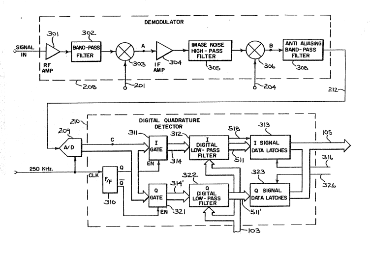
Figure 1 is a block diagram of an NMR system which employs
tha present invention;
Figure 2 is an electrical block diagram of the transceiver
which forms part of the NMR system of Figure 1;
Figure 3 is an electrical block diagram of the received
signal processor components in the transcei~er of Flgure 2;
Figures 4A-D are wave~orm~ of the recei~ed signal at
20 different stages of processing;
Figure 5 is an electrical block diagram of a digital
filter used to process the recelved slgnal; and
Figure~ 6A and B are a ~lowchart of a filter program for a
digital signal proce~sor in the low-pass fllter in Figure 3
~
Re~erring first to Figure 1, there is shown in block
diagram form the major components of a preferred NMR system
which incorporates the presen~ invention and which i5 sold by
the General Electric Company undex the trademark "S~GMA~. The
30 overall operation of the system is under the control of a host
: ., . ' . . . . .
~ ~ . . .................................. .
.
6~7
7--
computer sys~em generally designated 100 which includes a main
computer 101 (such as a Data General MV4000). The computer has
associated therewith an interface 102 through which a plurality
of computer peripheral devices and other NMR system components
5 are coupled. Among the computer peripheral device~ is a
magnetic tape drive 104 which may be utilizcd under the
direction of the main computer for archiving patient data and
images to tape. Processed patient data may also be stored in
an image disk storage device designated 110. The function of
10 image processor 108 is to provide interacti~e imaqe display
manipulation such as magni~ication, image comparison, gray-
scale ad~ustment and real time data display. The computer
system is provided with a mean~ to store ra~ data (i.e. before
image construction) utili7ing a disk data storage system
15 designated 112. An opera~or con~ole 116 is also coupled to the
computer by means of inter~ace ~0~ and provides the operator
with the means to input da~a pertinent to a patien~ study as
well as additional data necessary ~or proper NMR system
operation, such as calibrating, initia~ing and terminating
20 scans. The operator console is also used to dlsplay images
stored on disks or magne ic tape.
The computer system 100 exercises control over the NMR
s~stem by means of system control 118 and gradient amplifier
system 128. The computer 100 com~unicates with system control
25 118 by means of a communication data link 103 ln a manner well
known ~o thos~ sktlled in the art. The co~mNnication data link
103 consists of a parallel data bus, a parallel address bus and
a control slgnal bus. The syste~ con~rol 118 includes ~everal
subsystems such as a pulse contrQl module (PCMj 120, an array
30 processor 106, a radlo frequency transceiver 122, a status and
control modulP (SCM) 124, and the power supplie~ generally
designated 126 necessary to energize the component~. The PCM
120 utilizes control signals prov~ded by main computer 101 to
generate digita~ tlming and control signals Cuch as the digital
~` 35 waveforms which control gradient coil excitation, as well as RF
,~ :
:`
- . .,
-
' ' `
.
7~
envelope waveforms utilized in the transceiver 122 for
modulating the RF excitation pul~es. The gradient waveforms
are applied to the gradient amplifier system 128 generally
comprised of Gx, Gy and Gz amplifiers 130/ 132 and 134,
5 respectively. Each amplifier 130, 132 and 134 is utllized to
excite a corresponding gradient coil ln an assembly generally
designated 136 and which is part of a magnet assembly 146.
When energlzed, the gradient coils generate magnetic field
gradients Gx, Gy and Gz of ~he magnetic field in the same
lO direction as the main polarizing magnetic field, wherein the
gradients are directed in mutually orthogonal X-, Y- and Z~axis
directions of a Cartesian coordina~e system. That is, if the
magnetic field generated by a main magnet (not shown) is
directed in the z direction and i~ termed Bo~ and the ~otal
15 magnetic field ln the z direction i5 referred to as Bz, then
Gx = ~Bz/~x, Gy = aBz/~y and Gz = a~z/~æ, and the magnetic field
at any point (x, y, z) is given by B(x, y~ z) = Bo + GXX + GyY
+ GzZ.
The gradient magnetic fi~lds are utilized in combination
20 with radio freguency pulses generated by transcQiver 122~ RF
power amplifier 123 and RF coil 138 to encode spatial
inormation into the NMR signals emanating from ~he region of
the patient being studied. Waveforms and control signals
provlded by the pulse control module 120 are utilized by the
Z5 transce~ver subsystem 122 for RF carrier modulation and mode
control. In the transm~ mode, the transmitter provides a
radio frequency waveform modulated in accordance with the
control signals to an RF power amplifier 123 whlch then
energizes RF coll 138 which is situated within main magnet
30 assem~ly 146~ The NMR signals radiated by the excited nuclei
in the patient are sensed by ~he same or a different RF coil
than is used for transmitting and are co~pled to the `-
transceiver 122 by a preamplifier 139. The ~MR signals are
amplified, demodulated, ~iltered, and digitized in the receiver
35 section of the transceLver lZ2. The processed NMR signals are
. .
,
2~ 77
transmitted to the array processor 106 for processing by means
of a dedicated, unidirectional data l~nk 105.
The PCM 120 and SCM 124 are independent subsystems both of
which communicate with main computer 101, peripheral system,
5 such as patient positioning system 152, as well as to one
another ~y means of da~a communication link 103. The PCM 120
and SC~ 124 are each comprised of a 16-bit microprocessor (such
as Intel 8086) for processlng commands from the main computer
101. The SC~ 124 includes means for acquiring lnfoxmation
lO~regarding patient cradle position, and the position of the
moveable patient alignment light ~an beam (not shown). This
information is used by main co~puter 101 to modify image
display and reconstruc~ion parameter~. The SC~ 124 also
initiates functions such as actuatlon of the patient transport
15 and alignment systems.
The gradlent coil assembly 136 and th~ RF transmit and
receiver coils 138 are moun~ed within the bore of the magnet
utilized to produce the polarizing magnetic field. The magnet
forms a part of the main magnet assembly which includes the :
20 patient alignment system 148. A shlm power supply 140 is
utilized to energize shim coils associated with the main magnet
and which are used to correct inhomogeneities in the polarizing
magnetic field. In the case of a resistive magnet, a main
magnet power supply 142 is utilized ~o continuously energize
25 the magnet. In the case of a superconductive magnet, the main
power supply 142 i~ utilized to bring the polarizing field
produced by the m~gnet to the proper operating strength and is
then disconnected. In the case of a permanen~ magnet, power
supply 142 would not be needed. The patient alignment system
30 148 operates in combination wi~h a patient cradle and transport
system 150 and patient positioning system 1S2. To minimize :
interference from external sources, the NMR system components
comprised of the main magne~ assembly, the gradient coil
assembly, and the RF transmit and receiver coils, as well as
: ' :
;~ ,
~ .
;7~
--10--
the patient-handling devices, are enclosed in an RF-shielded
room generally designated 144.
Referring particularly to Figures 1 and 2, the transceiver
122 includes CompQnen~S which produce the RF excitation field
5 Bl through RF power amplifier 123 at a coil 138A and components
which receive the resultlng NMR si~nal induced in a coil 138B.
The base, or carrier, frequency of the RF excitation field is
produced by a frequency synthestzer 200 whlch receives a set of
digital signals ~CF) through the data communication link 103
10 from the main computer 101. These dlgital signals indicate the
frequency (e.g. 63.86 MHz) and the relative transmit to receive
phase of the RF carrier signal which is produced at an output
201. The commanded RF carrier is applied to a modulator 202
where it is modulated in response to a signal R(t~ received
15 through link 103 from the PCM 120. The signal R(~) defines the
en~elope of th~ RF excitatlon pulse to be produc~d. It is
produced in the PCM 120 by sequentially reading out a series of
stored digital values, that represent the desired envelope~ as
the RF excitation pulse is generated. These stored digital
20 values may, in turn, be changed by the computer 100 to enable
any de3ired RF pulse envelope ~o be prod~ced. The magnitude of
the RF excitation pulse output through line 205 ls attenuated
by a transmit at~enuator cir~ult 206 whlch receives a digital
slgnal, TA, from the main computer 101 through data
25 communication link 103. The attenuated RF excitatisn pulses
ar~ applied to the power a~pllfier 123 that drives the RF
transmitter coll 138A.
The NMR signal produced by the patlent is plcXed up by the
receiver coil 138B and applied to the input of a receiver 207.
30 The receiver 207 a~pllfies the NMR signal and this is
attenuated by an amount determined by a digital attenuation
signal ~RA) receive~ from the main computer 101 through link
103. The receiYer 207 ls also turned on and o~f hy a signal
through line 211 from the PCM 120 such that the NMR signal is
~: .
' ~ ~ .............. : , : :
.
2~ ;7~
acquired only over the time lntervals required by the
particular acquisition being performed.
The received NMR signal contains p~tient image information
within a 125 kHz band of frequencies centered at or around the
S Larmor frequ~ncy, which in the exemplary embodiment of the
present invention is 63.B6 MHz. One should recognize that the
primary image in~ormation of interest typically lies in a
narrower band within this 125 kHz band of frequencies. The
received high frequency signal ls ftltered and demodulated in a
10 two step process in a demodulator 208. Flrst the NMR signal is
filtered and mixed with a earrier signal on line 201, tha~ is
2.6875 MHz above the frequency center o~ the image information,
and the resulting difference signal is filtared and mixed with
the 2.5 MHz reference signal on line 20~. The r~sultant
15 demodulated NMR signal on line 212 ha~ a maxlmum bandwldth of
125 kHz and it is centered at a frequency o~ 187.5 kHz. This
~ignal is further filtered and applied to the input of an
analog-to-digital (A/D) converter 209 which samples and
dlgitizes the analog signal at a rat~ of 250 kHz. The ou~put
20 of the A~D converter 209 is applied to a dlgital quadrature
detector 210 which produce~ 2 32-blt in-phase ~ alue and a
32-bit quadrature (Q) value corresponding to alternate received
digital sample~. The resulting s~ream of dlgital I and Q
values of the received NMR signal i output through data link
25 105 to the array processor 106 where they are employed t3
reconstruct an image.
To insure the phase con~istency in the received N~R
signals in multlple imaging sequences, both the modulator 202
in the transmitter section and the demodulator 208 ln the
30 receiver section are operated with common or digi~ally
controlled signals. More par~icularly, the carrier signal at
the output 201 o~ the frequency syntheslzer 200 and the 2.5 MHz
reference signal at the output ~04 of the re~erenc~ frequency
generator ~03 are employed in bo~h the modulation and the
35 demodulation process. Phase consistency is thus maintained and
~'''' ~'
::
12 ~ 677
phase changes o~ the demodulated recei~ed NMR signal accurately
indic~te the phase changes exparienced by the excited spins.
The 2.5 MHz reference slgnal as well as 5, 10 and 60 MHz
reference si~nals are produced by the reference frequency
5 generator 203 from a common 10 MH7 clock signal, and the lat~er
three reference signals are employed by th~ frequency
synthesizer 200 to produce the carrler slgnal o~ output 201.
With reference to Figure 3, the signal from of the
receiver and attenuator 207 is applied to an RF amplifier 301
10 in the demodulator 208. The output of the RF amplifier 301 is
coupled to the input of a band-pass ilter 302 which passes a
one MHz band of frequencies that is centered at 63.86 MHz and
which has a 30 db re~ection of ~requencle~ outside this band.
For example, this filter may be a model 4LB32 manufactur~d by
15 K & L Mlcrow~ve, Inc. that is ad~usted ~o th~ proper frequency
response. The purpose o~ the band-pass fllter 302 is to remove
any noise outside a one ~Hz band of frequencie~ in which lies
the 125 kHz band containing the NWR image information. This
filtratlon insure~ ~hat the noise wlll not be intro~uced in~o
20 the signal next produced by heterodyning the image information
signal with a reference frequency si~nal. Alternatively, a
low-pass fil~er with the proper frequency responsa can be us~d
in place of band-pass filt~r 302.
In the receive mode, the frequency synthesizer 200 is
25 ad~usted to produce modified carrler signal on line 201 at
66.5475 ~z. The frequency of ~he carrler signal during the
receive mode is 2.6~75 MH~ higher than the center o~ the input
RF signal's frequency band of interest. It ls chosen so tha~
the image informa~ion will be centered at 1.5 times i~s maximum -~
30 bandwidth (125 k~z)in the demodulator output si~nal on line
212, as will be described. The modi~ied carrier signal is
heterodyned with the output of th~ band-pa~s filter 302 in a
first mixer 303. This mlxing generates a ~irst intermediate
frequency (I.F.) signal at node ~ with the image in~ormation
i
;
-. . ~ , .
,. ~ - :
,~
.- . . .
2~ 77
-13-
401 contained in a 125 kHz band of frequencies centered at
2.6875 MHz, as illustra~ed in Figure 4A.
The output of the first mixer 303 is coupled by an I~Fo
amplifier 304 to a high-pass filter 305. The response of this
5 filter 305 (depicted by the dashed line 402 in Figure 4A~ is
selected to remove noise below 2.50 MHz. Of particular concern
is the noise and extraneous signals 403 in a band o~
frequencies centered at 2.3125 MHz, ~hich band is symmetrical
about 2.50 MHz with the image information 401. For example,
10 filter 305 can be a model 968 ma~ufactured by Netcom, Inc. with
a pass frequency at 2.6873 MHz and having an amplitude response
of iO.1 db throughout a 62.5 kHz b nd on either ~ide of the
pass frequency and a 30 db re~ec~ion of frequencies below 2.375
MHz. If the noise and other ex~raneou~ slgnals helow 2.50 MHz
15 are not removed from the signal, subsequent heterodyning will
superimpose these unwanted signals onto the image infoxmation.
The output of the lmage noise high-pass filter 305 i5
applied to one input of a second mix0r 306. ~nother input of
the second mixer receive~ the 2.50 MHz reference signal on line
20 204 from the reference frequency senerator 203. The two
signals applied to mixer 306 hetexodyne to produce an output
signal at node B in which ~he 125 kHz band of frequencies
containing the image information now is cen~ered at ~87.5 kHæ,
as illustrated in Figure 4Bo
The resultant signal from the second mixer 306 is coupled
to an anti-aliasing band-pass filter 308. The response of this
filter 308 is repre~ented by the dashed trapezoid 404 in Figure
4B and is selected to remove noise from the signal at frequen-
cies above and below ~he band of image information frequencies.
30 The frequency response of filter 308 i~ substant~ally flat for
frequencies in the 12S kHz band centered at 187.5 kHz and has a
50 db rejection of frequencies beyond 81.25 kHz o~ either side
of the center frequency. For example, this filter may be a
model 944 manufactured by Netcom, Inc.
.
,,, ~ . -
,, - ,. . .
. : : . , ~ ::
2t~677
-14-
Referring still ~o Figures 3 and 4A-D, the filtered signal
is then coupled to the input of the analog to digi~al con~erter
209, which pexiodically samples the signal and produces a
digital representation of the signal sample amplitude. The
S Shannon Sampling Theorem states that the sam~ling rate must be
at least twice the bandwidth of the analog signal. ~f this is
not done, some frequency componen~s of the analog signal will
be superimposed, i.e. will be indlstinguishable from each other
in the sampled data. This phenomenon is called "aliasing~'.
10 When applied to analog signals, (e.g. a low-pass signal with
frequency content between 0 to 250 kHz), this theorem dictates
that the sampllng rate be at least twice the highest frPquency
present (i.e. a sampling rate of 500 kHz). However, in the
present band-pass case, with a bandwldth equal to half the
15 highest frequency present, the sampl~ng rate need not exceded
250 kHz, a~ will be further described belowO
If the input to analog to digital converter 209 is viewed
as a low-pass signal, i.e. 0 to 250 kHz, a sampling rate of
250 kHz undersamples the image information data. This under
20 sampling of the signal intentionally aiiase~ the image
information component, reflecting ~re~uencie~ be~ween 125-250
kHz into the 0-125 kHz band, flipped end-for-end in the
frequency direction. The resul~ of the aliasing i5 depicted
graphically by the waYefonm of Figure 4C. I~ should be
25 remembered that the anti-aliaslng band-pass filter 308
essentially removed all signal components le.g. noise) in the
0-125 kH2 band, a~ well as at frequ~ncies above 250 kHz.
Therefore, the digitized slgnal contains lnformation prlmarily
due to the amplitude of the ~requency components in the 125-250
30 kHz band, i.e. the frequencies which contain NMR image
information. Without the anti-aliasing filter 308, noise and
other signals in the 0-125 kHz band would be superimposed onto
the image information by the digitizing process. Because the
frequency cutoffs of the anti-aliasing band-pass filter 308 are
35 not step functions, spurious signals just below 125 kHz and
, . . ., -. - , . -,
F . .
2~0Ei77
-15-
just above 250 kHz may not be ~ully attenuated. However, since
the primary image information of interest typically lie~ in a
narrower (e.g. 32 kHz) band centered a~ 187.5 kHz, these
spurious signals will not adversely affect the constructed NMR
5 image.
The demodulator 208 and the analog to digital converter 209
shift the frequency band of the image information to near
baseband frequencies and diyitize ~he signal~ Although the
signal which results from this processing could be used directly
10 by an array processor 106 ~see Figure 1) to construct an image,
it is desirable to derive two standard quadrature signals tI and
Q) containing the image in~ormation in order tha~ a con~entlonal
array processor can be utili~ed.
The remaining portion of Figure 3 shows the components of
15 the quadrature detector 210. This circuit produces the I and Q
quadrature signals ~rom the diglti~ed image information signal
and essentlally brings the mld-frequency (62.5 kHz) of the
digitized signal down to dc level ~i.e. zero ~artz in Figure
4D). The quadrature detec~or 210 al50~ dlgltally filters the I
20 and Q slgnals to remove extraneous frequencie~. ~
The classlcal quadrature d tec lon technique involves
separa~ely mixing every sample ~rom the analog ~o digital
converter 209 with sine and cosine reference signals at ~he
62.5 kHz mld-band fr~quency. Since the sampling rate of the
25 analog to dlgl~al converter for the imaga information signal
is 250 kHz, the sine and cosine ref~rence slgnals must also be
sampled at that rate to provlde dlgltal values by which to
multiply the ~mage lnformation samples O Th~ sampling frequency
ls ~our times the frequency of the~reference signals and has~a
30 phase relationship, which produces the following series of
d~gital values for the cosine and slne re~erence signals:
cosine: 1, 0, -1, 0, 1, 0, -1, 0,...
sine: 0, 1, 0,~ -lf~0, 1, 0, -1,. o ~ '
:~:
:.
' `. ' : :
~16-
As can be observed from ~hese numerical series, when the
image informatlon sign~l is multiplied by the cosine and sine
reference slgnals every other produc~, or term in the resultant
I and Q signals, will be zero. As a co~sequence, part of the
5 quadrature detection can easily be implemented by a pair o~
gates which alternate passing every other image information
signal sample, recognizing that the ~nterleaved zero terms are
not present in the gated ou~puts. That i5 when the "I n gate is
open to pass an image information sample, the l'Q" gate is
10 closed: and vice versa. However, every fourth term of both the
sine and cosine numerical series is a negative one, which means
that every other time that each gata is opened the sample
should be inverted, or negated in digital terminology.
Referring still to Figure 3, the dlg~tized ima~e signal
15 samples from the analog to digital converter 209 are applied to
the inputs of two sets of logic gates 311 and 321. The first
set of logic gates 311, designa~ed a~ the I g~te, are rendered
conductive by a clock signal from the Q output of flip-flop
~F/F) 310. The second set of logic gates 321, de~ignated as the
20 Q gate, are re~dered conductive ~y a clock signa} from the Q
output of flip-flop 310. The flip-flop is clocked by the 250
XHz signal that also is applied to the analog to digital
converter 209. S~nce Q and Q are complementary signals, each I
and Q gate 311 and 321 will be conductive on alternate pulses of `~
25 the 250 kHz re~erence signal with only one of them being
~ conductive at any given time. This alternate clocking o~ the I
i and Q gate sets perform~ the quadrature detection, with the
exception o~ negating the si~n o~ every other sample passed. As
w~ll be described, this latter func~ion is accomplished by
30 subsequent digital low-pass ~ilters in the quadrature detector
210, which change the sign of every oth~r sample i~ the I and Q ~-
channels.
The outputs of the I and Q signal gate 311 and 321 are
coupled to separate low-pass, finlte impulse response ~FIR~
35 digital filters 312 and 322, respectively. These I and Q
,:''
2q~ i7~
-17-
low-pass filters are implemen~ed by two identical circuits,
which ca~ digitally compute con~olu~ion opera~ions with up to
255 taps. As a signal sample ls applied to one of the filters
312 and 322, it enters the first stage of an N stage pipeline
5 in which each s~age represents a tap of the filter, and with
previous samples being shifted one stage down the pipeline. A
filter tap coefficient is defined for each stage. ~hen a
filter output value is desired, the tap coefficients are
multiplied by the signal samples in the corresponding ~tages.
10 The produets of these multiplications are summed to produce the
~ilter output vàlue.
As a result of the funetion of I and Q ga~es 311 and 321,
the low-pass filters 312 and 322 are presented with all the
non-zero data that would result from multlplicatlon of the
15 incoming image informa~ion signal ~amples with the samples
cosine and sin~ reference slgnals. However, the~e ~ample are
not in time synchrony. Suppose the ga~e logic is arranged so
that the first sample of the analog to d~gital converter 209 is
passed by ~he I gate 311 to low-pas~ er 312. The
20 corresponding Q data sample would be zero and is not seen by
the Q low-pass filter 322. The next sample from the analog to
digital conv~rter 209 is passed by Q gate 321 to the Q low-pass
filter 322. As a result, the first data point in the I
low-pass filter 312 precedes th~ first data point in ~he Q
25 low-pass filter 322 by one sampling period. If compensation
for this temporal difference is not pro~ided, the outputs of
the I and Q filters will no~ be interpre~able as conventional I
and Q data pair~, which are typically in time synchrony. ~ .
However, compensation for thls relative lag of Q data
with respect to I data is easily p~rformed as part of the
low-pass filtering operation by uslng diffare~t se~s of filter
coefficients in the I and Q digital filters 312 and 322.
Knowledge of the frequency content of the signal ou~pu~ of ~he
anti-aliasing band-pass filter 308 is used to compu~e ~IR
filter using ~nown techniques and a sampling rate of 250 kHz.
~.
.
~ .
- , ~ ~ -,
. ,~ , : .
.
.
~ 7 7
-18-
Let these coefficiants be If1, f2, f3~ ... fN~- Conven~ional
digital implementation of quadrature detection and low-pass
filtration would be as follows. For the I channel, samples from
the analog to digital conver~er 209 would be multiplied by a
5 cosine reference signal. Simultaneously, digital samples would
also be multiplied by a sine reference signal. This parallel
multiplication generates a pair of sine and cosine reerenced
products. At any time that a low-pass filtered I, Q data pair
is desired, the N most recent cosine re~erenced products would
10 be pairwlse multiplied by the filter coefficients {f1, f2, f3,
... fN} and then summed to produce a filtered I value. Also,
the N most recent sine reference products would be pairwise
multiplied by the filter coefflcients ~f1, f2~ f3~ -- fN} and
summed to produce a filtered Q value. ThiS I, Q data pair could
15 be used in the conventional manner to construct an ~MR image.
However, recall that every other sample of the cosine and
slne reference.slgnals is zero, and therefore so are the
corresponding cosine and sine referenced products. Thus, half
of the values summed in a con~entlonal filtering operation would
20 be zeroes. These needless steps can easily be bypassed.
Suppose that at the time a filtered I, Q data paix is
desired the most recent cosine re~eren~ed product is non~zero.
As is clear by now, only pairwise multlplication of the cosine
referenced signals with the odd numbered coef~icients in the
series {f1~ f2~ f3' fN} would have non-zero products. The
entire operation is equivalent to using only every other output
of the cosine referenced products ~the non-zers ones), pairwise
multiplying these N/2 values with th~ alternate coefficients
25 {fl, f3, f5, ~ , and su~ming the N/2 produc~s. Similarly,
only the non-zero sine referenced values need be considered,
which are multiplied by the even numbered coef~icients {f~, f4,
f6, . . . } and the N/2 products then are summed to produce a
filtered Q value.
?
'.
' ~ '. ' :
i7~
--19--
It is seen, then, ~hat the complete digital quadrature
demodulation and low-pass filtration can be equivalently
accomplished by passing alternate outputs of the analog to
digital converter 20~ to I and Q clrcuits, negating every second
5 sample of each, and operating on each I and Q sampla set with
somewhat different FIR filters. The coefficients for each FIR
filter 312 and 322 are ~imply al~ernate terms of a con~entional
FIR filter coefficient serie~. The simplification in processing
results from the fact that the demodulation frequency is one-
10 quarter the sampling frequency, and tha~ tha phase of the cosineand sine references was chosen so tha~ their alternate samples
are zero.
The I and Q low-pass filters 312 and 322 are implemented
by two identical circuits with the circuit for the I signal
15 filter 312 as shown in F~gure 5~ The filtering process is
performed by a digital signal processor ~DSP) 502, ~uch as a
TNS320C25 model manufactured by Texas Instruments, Inc. The
TMS320C25 digltal signal processor contalns a 32-bit arithmetic
loglc unit and accumulator, on chip memory (~AM and ROM) and
20 external memory access capability. Thls DSP is a programmable
device which enables the I and Q signal~ to be processed in
real-time according to known digital signal processing
algorithms. Specifically, the DSP applies digital filter
coefflcients to the I or Q si~nal to remove noise and spurious
25 signals at frequencies which do not contain imag~ information~
The DSP 502 allowR different f~lter characteristlc to be
applied to the I slgnal by software selection of different sets
o~ filter coefficients.
The program executed by the D5P 502 to per~orm the
30 filtering and the digital fllt~r coeffictents used by that
program are stored in a random access memory (~AM) 504. The
program and coefficients are downloaded over communication link
103 from the main computer system 100 into RAM 504 upon power-up
~ of the NMR imaging system. As noted previously, thls link 103
¦ 35 consists of a data bus, an ad~ress bus and a control signal bus.
~: :
. . ,
-20-
The data bus is connected to a set of data buffers 506 which
interfaces communica~ion link 103 ~o a filter data bus 511. The
filter's da~a bus 511 extends to the I data latches 313 so that
the output from the filter can be stored in the latches.
5 Similarly, the address bus of the communication li~k 103 is
interfaeed to a filter address bus 512 by a set of address
buffers 50~. The data and addres~ buffers 506 and 508 are
enabled by a signal on a line o~ th~ control bu.~ 513 when the
program and filter coefficients are being downloaded.
The signal samples passed by th~ I gate 311 are applied
via a set of lines 3~4 to the data inputs of a 512 stage FIFO
register 514. The FIFO register S14 provides an asynchronous
dual-access register for isolating the I signal gat~ from the
filter data bu~ 511, thereby enabling the DSP 502 to operate in
15 a uninterrupted manner. When DSP 502 requires an I signal
sample, the output from the signal sample ~FO register 514 i5
coupled to the filter data bus 511 in response to a xignal from
the control bus 513.
A filter control clrcuit 518 governs whlch components are
20 electrically coupled to filter data bus 511 and address bus 512
at any given time. For this purpo~e, the filter control circuit
responds to commands from the DSP 502 by producing control
signals on bu~ 513 for specific components~
The progræm which i~ executed by he DSP 502 to per~orm
~5 the digital filtering is wrlt~en in a eon~entional manner by
standard programm~ng techniques using documen~ation and program
development so~tware avallable from the manufacturer of the
DSP. For example, Texas Instruments, Inc. provides such
matertals for progxamming the TMS320C25 model digi~al signal
30 processor.
The digital signal processor program is depic~ed by the
flowchart in Figures 6A and 6B. The program begins an :~
execution cycle when the DSP 502 receives:a signal indicating
tha~ a new NMR data frame is being process~d. In the first
35 step 601 of the filtering process, the DSP is initialized. The
~ 67 7
-21-
filter may be configured to decimate the amount of signal data
by requiring the input of a gi~en number of signal samples into
the filter before each output value is produced. At step 602,
a decimation count of input signal samples used by this
5 function is zeroed. Data, previously received from the
computer system 100, are then used at step 603 to configure ~he
filter by selecting one of several sets of filter tap
coefficients stored in RAM 504, the decimation amount and other
parameters. An internal DSP buffer, which stores the I signal
lO samples for each tap of the filter, is cleared of any residual
samples from the previous ~ata frams ~t step 604
The diqital signaL processor 502 then issues a control
signal to read the first signal sample from the FIFO register
514 at step 606. As noted previously, every other image
15 information signal sample passed by th~ set of I gates 311
should be negated, but the I gate can not perform that
negation. Therefore, a quadrature sign flag i~ te~ted at step
608 to determine if the curr~nt sample should be negated. If
the flag is set to a high logic level, the program execution
20 ~umps to step 612. However, if the quadrature sign flag has a
low logic level, the sign of the signal sample is changed at
step 610. Then the quadrat~re sign ~lag i~ togglad at step 612
to indicate whether the next I signal sample should be negated.
Alternatively, the negation here and at steps 630-634 can be
25 accomplished by negating the proper filter coe~ficients stored
in ~AM 504.
Prior to computing an output value for the filter, half of
the filter taps (e.g. 128 taps for a 255 tap filter3 must be
prefilled wi~h signal sample~. A~ step 614, a counter is
30 checked by the DSP 502 to determine if hal~ o~ the filter ~aps
have been prefilLed. If the prefilling is not complete, the
program execution branches to step 616 where the current signal
sample is stored in the location~of a sample buffer withln the
internal memory of the DSP, which location i~ indicated by a
35 pointer. The buffer pointer is incremented at step 618 before
:?
" ` : ~ , , ' `
.~ ~
' ~
-22~ 7~
the program execution returns to step 606 where another signal
sample is obtained from the FIF0 reglster 514. Th~ program
execution continues to loop through steps 606 618 until half of
the taps of the filter have been pre~llled.
At this time, the program ad~ances from s~ep 614 to step
620 where the current I signal sample i5 stored in th~ filter
buffer~ Then, at step 622, the buffer pointer is changed to
indicate the address of the last buffer storage location,
thereby pointing to the oldest sample in the buf~er. However,
lO since only half of th2 taps have been prefilled, initially the
last buffer locatio~ will contain a zero value. Because
physlcally shif~ing the samples wlthln the buffer is a time
consuming operation, the signal samples are stored 1n a rlng of
storage locatlons within the buffer. A~ a new sample is fed to
15 the filter, it overwrites the oldest sample as indlcated by ~he
pointer at step 620 and the polnter ls changed to the nex~
oldest sample around the ring a~ s~ep 622. AS will be
described, in applying the tap coe~ficien~s to the stored
samples, the coeff~cient for the last fil~er tap is applied to
20 the sample indicated by the pointer, and each subs~quent tap
coefficient is applied to the next storage location around the
buffer ring.
At step 624, the DSP 502 checks the decimation count
stored in its memory to de~ermine whether ~he count equals
25 zero. As noted previously, the signal data may b~ decima~ed by
inputting a given number of ~iynal samples lnto the fil~er for
each output value that is produced. This giv~n number of input
samples i5 indicated by a decimation parameter stored in RAM
504, which is used to reset the decima~ion count. If the
30 decimation count is a non-zero Yalue, an output of the filter
is not calculated. Ins~ead the program branches to step 626
where the decimation count is decremented. The program then
advances to step 628 where the next I signal s~mple is obtained
from the FIFO register 514. ~s with the prefill samples, every
35 other sample has to be negated. At step 630 the quadrature
.
- , ~ . ~ . . .
2(~ ;77
-23-
sign flag is tested and if necessary, the sample i5 negated at
step 632. The flag is then toggled at s~ep 634 before the
program execution returns to step 620 to store the sample.
The program continues to loop through steps 620-634 until
5 the decimation count is zero, at which time the execution
branches to step 636 where the decimation count is reset to the
parameter value. Then the digi~al signal processor 502
calculates a filter output value at step 638 by multiplying
each filter tap coefficient by the signal sample stor~d in the
lO buf~er location for the corresponding tap. The products of the
multiplication for each tap are summed to provide a dig1tal
output value for the filter. If necessary, the level of the
digital output value may be shifted at step 640 according ~o a
parameter supplied by the computer system 100 during set-up of
15 the filter.
At step 642, the computed output ~alu~ for the filter 312
is applied by ~he DS~ 502 to the ~iIter da~a bus 511, and an
input enable signal is set via line 518 of the filter control
bus 513 to the I signal data latches 313. This input enable
20 signal causes the data latches 313 to store the filter output
value then presen~ on data bus 511.
The DSP 502 then determines if a~other signal sample
exists in the FIFO register 514 at step 644. If such a sample
is ~o~nd, the program executlon branches to step 628 to obtain
25 and proces~ the sample. The fllterlng process repeats until
all of the signal samples have been f~ltered at which point the
program ends.
Wlth referenc~ to Figure~ 1 and 3, as the digital ou~put
values from the I and Q digital low-pass filt2rs 312 and 322
30 are stored in the sets of data latches 313 and 323, the pairs
of I and g value ar~ selectively read over data link 105 by
the array processor 106. A signal on control lines 316 and 326
from the array processor 106 enable~ the ou~put from I and Q
data latches 313 and 323, respectively. The data latches are
35 FIFO devices which enable the I and Q value3 to be buffered.
..
,
. . .
-24- 2 O ~O 6q 7
This bu~fering allows the array processor 106 to work
asynchronously of the I and Q circuitsO