Note: Descriptions are shown in the official language in which they were submitted.
~' 26~ 9S6
BAÇKGROUND OF THE INVENTION
1. Field of the Invention
The present invention relates to logic circuitry and, more particularly, to
5 logic circuitry used to provide extremely rapid switching between output display
frames in a computer system.
2. Discussion of the Prior Art
As computer systems such as work stations have grown more and more
10 sophisticated, it has become clear that they might be conveniently utilized for
providing the animation features that one associates with motion pictures and
television. A computer which is capable of providing an animated output offers adistinct advantage over television and motion pictures because it, unlike the
others, allows both the construction and revision of the images of animated
15 displays. The ability of computers to provide three dimensional displays has
hastened and heightened the desire for systems which are capable of handling
animated subjects.
, ;.
` A major problem in utilizing computers to provide animated output is that
, 20 animation requires the display of frames which vary by small increments and
succeed one another in rapid sequence. In order to display a single frame of
graphical material on a cathode ray tube (CRT), it is necessary to store an
indication of the information for each position (pixel) which is to appear on the
output display. With large and detailed displays, the number of pixels on a
- 25 cathode ray tube may average approximately one thousand in a horizontal
direction and a like number in the vertical direction giving a total of approximately
,~ - one million pixels about which information needs to be stored for each frame. In a
- preferred system which is capable of providing a number of different colors and
hues on the cathode ray tube, twenty-four bits of digital information specifying30 the particular color output are stored for each pixel of the display. Consequently,
approximate!y twenty-four million bits of information need to be stored for eachframe to be presented at the output. This requires a substantial amount of time.
82225.P054
201 0966
Moreover, not only does writing the approximately twenty-four million bits
for each frame require a substantial amount of time, but the clearing of those bits
in order to present the next frame requires an additional amount of time. Some of
the delay between frames has been obviated by using double buffered systems
5 in which two full screen bitmapped display memories are provided and switched
alternately to the cathode ray tube output. Such a system reduces substantially
the time between presentation of two frames of information but does not eliminate
the need to clear each of the display memories so fhat it may be written with the
color information for the frames which follow. Consequently, even such double
0 buffered systems are too slow to provide optimum outputs for animation purposes.
An arrangement for decreasing the delay between individual frames is
described in copendin~ Canadian patent application serial no. 599,864,
Apparatus for Rapidly Clearing the Output Display of a Computer System, Joy et al.,
filed May 16, 198g, and assigned to the assignee of the present invention.
This arrangement decreases the delay by essentially eliminating the time
normally used for clearing the display memories in such a system. The system
accomplishes this by providing full frame double-buffered bitmapped memories in
which are stored indications that the information in the same position of an
20 associated display memory part of in a particular frame. These memories are
referred to as frame identification memories or buffers. Consequently each
position representing a pixel in the twenty-four bit display memory has an
associated, corresponding position in a four bit frame identification memory
which identifies it by frame number.
~" 2 5
- When a frame which has been written into the display memory is to be read
out, an output frame identification register is given the number of the frame to be
read out; and that frame number is compared with the value of each position in
the frame identification memory as the frame identification memory and the
display memory are scanned for cathode ray tube refresh. Only those pixels
which are in the selected frame are provided as output from tha display memory
to the cathode ray tube. At display memory positions at which the frama number
in the output frame identification register and the number in the frame
82225.P054 -2-
9~i6
identification memory do no~ compare, a background color generator is activated
to provide background color to the display. This allows frame-to-frame writing to
the display memory to continue without clearing the display memory while
clearing only a small portion of the frame identification memory. This dramatically
5 reduces the intra-frame delay.
However, even this new arrangement offers an area for improvement
because, even though lhe twenty-four bit display memories need not be cleared
between frames, the pair of four bit frame identification memories must be cleared,
10 either completely or in portions, before the next frame may be written. Moreover,
although the use of frame identification memories allows the system to operate
without clearing the larger display memories, it does add a significant amount of
additional memory hardware to the computer system for use as frame buffer
memory.
It is, therefore, an object of this invention to improve the speed at which
images may be switched from frame to frame and presented at the output of a
computer system.
It is another object of this invention to substantially reduce the delay
associated with clearing frame identification memories between frames in a
.~ computer system.
It is another object of this invention to reduce the amount of memory
25 hardware required to implement a frame identification memory in a computer
system.
An additional object of this invention is to improve the speed at which
computer systems operate.
82225.P054 -3-
201 0966
SUMMARY OF THE PRESENT INVENTION
l The foregoing and other objects of this
invention are accomplished by a computer output system
comprising 3 first full screen bitmapped memory, a second
full screen bitmapped memory, apparatus for providing
input signals for writing information to be displayed by
an output device to each position of the first memory,
apparatus for storing in the second memory the positions
of each position of the first memory to be written to the
output device, and apparatus for comparing the signal
stored at each position of the first memory and the signal
: stored at the same position of the second memory to
: determine whether information at the position is to be
written to the output device.
Accordingly, in one aspect the invention resides
in a computer output system for rapidly displaying a
plurality of individual frames of information on display
. means including a display, comprising a first and second
: pixmapped display memories comprising a first and second
plurality of pixel storage positions for storing a first
and second frames of said frames of information; a
i pixmapped frame identification memory comprising a third
~ plurality of pixel storage positions simultaneously
corresponding to said first and second pixel storage
positions for storing a plurality of n-bit frame
indications, each of said n-bit frame indication
indicative of one of said individual frames of
information; input means coupled to said first and second
display memories and said frame identification memory for
:
: -4-
20 1 Oq66
1 alternately inputting said first frame and its n-bit frame
indication into said corresponding first and third
plurality of pixel storage positions, and said second
`~ frame and its n-bit frame indication into said
corresponding second and third plurality of pixel storage
positions; comparison means coupled to said frame
identification memory and said input means for comparing
said n-bit indications stored in said third plurality of
. pixel storage positions, said n-bit indication in said
input means and an indication indicative of a particular
frame to be displayed on said display in a predetermined
manner, and outputting enabling signals for said first and
~ second plurality of pixel storage positions if said
indications compare successfully under said predetermined
. 15 manner at said corresponding third plurality of pixel
storage positions; and control means coupled to said first
and second display memories and said comparison means for
selecting one of said first and second frames stored in
said first and second plurality of pixel storage positions
and displaying said frame information of said selected
frame stored at said pixel storage positions based on said
enabling signals.
These and other features and advantages of the
present invention will become apparent to those skilled in
25 the art after having read the following detailed
description ;n conjunction with the several figures of the
drawing in which like elements have been referred to by
like designations throughout the several views.
-4a-
.~
20 1 09b6
IN THE DRAWIN~
.
Figure 1 is a block diagram illustrating a prior art arrangement for
selecting individual frames to be displayed on a computer output device.
Figure 2 is a block diagram illustrating an improved arrangement in
5 accordance with the invention for selecting individual windows to be displayed on a computer output device.
~`
Figure 3 is a table useful in illustrating the operation of the arrangement
shown in Figure 2.
Figure 4 is a truth table illustrating the flow of signals in the arrangement
of the invention shown in Figure 2.
:.
-4b-
2~ 9~>6
p~LED QES~I~IPTION OF THE DR~WINGS
1. prior Ar~ Fram~ç~ cation Sys~çm
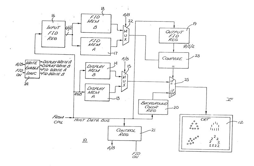
Referring now to Figure 1, there is shown a display output system 10 for
5 processing information rapidly; this system is disclosed in the above-mentioned
copending patent application. For the purposes of this explanation, a frame
means a particular graphical or data structure which it is desired to present as a
full screen presentation on a cathode ray tube or other computer output device.
The system 10 operates under control of a central processing unit (CPU) not
0 shown in Figure 1.
When it is desired to write a particular graphic frame to an output device
such as the cathode ray tube (CRT) 12 shown in Figure 1, the actual information
to be displayed is written to a display memory. The system 10 comprises a first
,.i 15 display memory 13 and a second display memory 14. The use of two display
memories in parallel, the output of which may be selected by a multiplexer 15,
allows the rapid switching between frames of a display which is necessary to
accomplish animation. In the usual case in which the system is used for
animation, a frame is written to display memory A while the frame in display
20 memory B is being furnished as output to the cathode ray tube 12. The
information in the frame in display memory A is then furnished as output to the
cathode ray tube 12 while a new frame is written to display memory B.
To obviate the loss of time incident to clearing the large display memories
25 and provide the switching speed necessary for animation, the output system 10of the copending application also includes an input frame identification (FIDJ
register 16, a pair of frame identification (FID) memones 17 and 18, an output
frame identification (FID) register 19, a background color register 20, and a
control register 21. The system 10 also includes a multiplexer 15 for selecting
30 one of the display memories, a multiplexer 22 for selecting one of the frame
memories, a comparator circuit 23, a write enable logic circuit 24, and a logic
circuit 25. It should be noted that the frame memories 17 and 18 are labeled A
82225.P054 -5-
2~ 966
and B, respectively; they are each associated- with the similarly labeled one ofthe display memories 13 (A) and 14 (B).
The operation of the system 10 is as follows. The CPU writes a value to the
5 control register 21 using the host data bus to select to which of the FID memories
17 or 18 and its associated display memory 13 or 14 it is to write. The CPU thenprovides a frame identification number which is stored in the input frame
identification register 16; this number is used for all of the information to be written
for this frame. In a preferred system, sixteen frame numbers (0-15) are utilized.
10 After the input frame identification register has been initialized with the frame
number, the actual information to be displayed on the output device is sent fromthe CPU to the selected full screen bitmapped display memory 13 or 14. The
frame identification memories 17 and 18 are also full screen bitmapped memories,each receiving input from the input FID register 16 and providing outputs to themultiplexer 22 so that signals may be rapidly switched for the presentation of
animated graphic images.
," .
Each piece of input information on the host data bus from the CPU carries
' a pixel address and color information (an RGB color value, for example).
;- 20 Presuming that the display memory A and the FID memory A have been
selected, the RGB color value is written to the appropriate pixet address in
- display memory A while the frame identification number is written to the same
: pixel address in the frame identification memory A. In a preferred system, the
frame identification number requires four bits of storage while the RGB color
value requires twenty-four bits of storage at each pixel.
. .
Consequently, when any particular full frame has been written to display
memory A, the display memory A contains, at the addressed positions chosen for
the particular frame, the representation to be displayed in RG8 color values while
30 the frame identification memory contains the frame numbers stored at the same pixel addresses.
82225.P054 -6-
- -
2~ `fj
When it is time to display a particular frame, the CPU, using the host data
bus, stores the selected frame identification number in the output frame
identification regis~er 19. The CPU also writes to the control register 21 so that
- the multiplexers 22 and 15 controlling the outputs of the frame identification
5 memories and the display memories, respectively, are set to select the output
from memories A. Then, as each pixel position in the display memory A is
scanned to the output through its associated multiplexer, the frame identification
value is also scanned from the frame identification memory A for that pixel
position. The comparator circuit 23 compares the output of the selected frame
identification memory and of the output frame identification register 19 and
provides a signal indicating those pixel positions of the frame identification
memory A where the selected frame has been written; this causes the RGB color
: signal stored at those positions of the display memory A to be furnished to the
cathode ray tube by the logic circuit 25. At all pixel positions other than those
properly identified by the frame identification memory A, the comparator circuit23 provides an output causing a background color to be furnished by the
background color register 20 and transferred to the cathode ray tube 12.
This arrangement for processing signals has a number of significant
20 advantages. For example, the system requires that color values be stored in the
display memories only at positions indicative of foreground data. Background
colors need not be stored in the display memories. Consequently, storage of
information may proceed at a more rapid rate than with the usual system where
twenty-four bits of information must be stored at each pixel. More importantly, a
25 display memory need not be erased after the information for a frame is read out in
order to write the next frame in that memory.
For example, after a first frame has been processed as explained above,
the next frame to be processed by the particular FID memory has a different frame
30 number so information written to the associated display memory is simply written
on top of the information already stored because the only information which willultimately be furnished to the display for a particular frame is the informationassociated with the selected frame number.
82225 P054 -7-
9~i~
It should be noted that the output system described with respect to Figure
1 may conveniently be utilized in a computer system which makes full use of
multiple windows and may also incorporate apparatus for providing output
. 5 indicative of the depth of each pixel provided for a particular display on the
cathode ray tube.
Although the use of FID memories and registers allows the system to
function without clearing the display memories between particular frames, the
number of bits utilized in the frame identification number system, four bits in the
preferred case, determines how many total frames may be written before the FID
memories themselves must be cleared. With four bits of digital slorage to recordthe frame number, sixteen total frames may be utilized. If the FID memories have; not been cleared after sixteen frames, then it is possible that information relating
to a previous frame will remain in an FID memory as the frame is again reached.
Since this information might be erroneous, the system does require that the FID
memories be cleared at least once in each sixteen uses.
'
An advantageous way of accomplishing the clearing without slowing the
` 20 operation of the system to any extent is to clear at least one-fifteenth or greater of
an FID memory after each frame is written to the output device. Such a system isdescribed in the copending patent application.
:
In the preferred embodiment of the arrangement described which clears
only one-fifteenth of the FID memories, the time utilized for clearing is
substantiatly less than that required by prior art systems having equivalent
display memories. Consequently, it is apparent that a system utilizing frame
buffers is especially useful in providing the rapid switching necessary to
-` animation.
2. The System Of the l~vention
Referring now to Figure 2 there is shown an improved system for rapidly
clearing the output display of a computer system. The system 30 shown in Figure
82225.P054 -8-
2 includes a pair of display memories 13 and 14, an output multiplexer 15, an
input frame identification register 16, an output frame identification register 19, a
background color register 20, and an output multiplexer 25, all similar to thoseshown in the system 10 illustrated in Figure 1. The system 30 also includes a
single frame identification memory 17 instead of the double buffered frame
identification memory of the system 10 shown in Figure 1.
As with the system of Figure 1, the display. rnemories 13 and 14 are, in the
preferred embodiment, each provided with twenty-four bits of storage at each
position which represents a pixel on the output display 12. In contrast to the
system disclosed in Figure 1, the input FID register 16 and the output FID register
19 each include only three bits of storage at each position. Moreover, the frameidentification (FID) memory 17 is provided with a similar three bits of storage at
each posi~ion representing a pixel on the output display; otherwise, the frame
identification memory 17 is essentially identical to either one of the two frameidentification memories 17 and 18 utilized with the system 10 shown in Figure 1.
The FID memory 17 of the preferred embodiment of the present system 30,
utilizes only three bits of memory for the because the clearing operation
proceeds at such a rapid rate that it is not necessary to utilize sixteen individual
frames in the FID memory 17. Three bits of memory allow a total of eight frames to
be utilized, a number found to be sufficient and especially economical.
.
In attempting to reduce the amount of memory utilized from the double-
: 25 buffered full-screen bitmapped frame identification memories disclosed in Figure
1 to the single frams identification memory used in the system 30 of this invention,
a major problem is encountered. In order to be able to switch rapidly between
display memories to present individual frames on the output display at a rate
sufficient for animation purposes, it is necessary to write to one of the display
memories and its associated frame identification memory while the information inthe other frame display memory is being written to the output display. This
requires that a comparison be made of the number stored in the output FID
register and that at each of ths pixel positions in the frame identification memory
82225.P054 -9-
2~9~i~
used with the display memory being written to the display at the same time that
the new frame identification number is being written into the frame identification
. memory for the new frame being stored in the other display memory. Since this
requires both writing to and reading from frame identification memories at the
5 same time, the system 10 of Figure 1 cannot simply utilize a single frame
identification memory. That is, the system 10 of Figure 1 cannot have its frame
identification memory hardware reduced in size or be made more rapid by the
simple expedient of using only a single frame identification memory.
This problem of both reading and writing to the same memory has been
overcome in the present invention by logic circuitry which solves the problem ofthe need to both write to and read the same memory at the same time. The logic
circuitry includes a full screen bitmapped display select plane (DSP) memory 32.The DSP memory 32 includes only a single bit of storage at each position
15 representing a pixel on the output display 12. Signals are furnished to the DSP
memory 32 from a comparator circuit 34. The circuit 34 compares each position
in the FID memory 17 with th~ FID number stored in the input FID register 16 less
one. A one is written to a position in the DSP memory 32 if the number in the FID
register 16 is one greater than the number at the position in the FID memory 17
- 20 indicating that a next greater frame is being written to the display memory;
otherwise, a zero is written to the position in the DSP memory 32.
Also added in the system 30is a second comparator 36 which compares
the frame identification number in positions of the FID memory 17 to the number
25 stored in the output FID register 19 plus one. This comparator 36 produces a one
if the number in tha output FID register 19 is one less than the number in the
compared position in the FID memory 17. Finally a comparator 23 compares the
number in the output FID register 19 with the number at the position scanned in
the FID memory 17 and produces a one if the numbers are equal.
The signals from the two output comparators 23 and 36 are each furnished
to A and B input terminals, respectively, of an output logic circuit 38. Also
82225.P054 .10-
2~3~09~ -
, furnished to a C input terminal of the output logic circuit 38 are the signals stored
in each position of the DSP memory 32.
The output logic circuit 38 may include gating circuits or other logic well
5 known to the prior art to provide an enabling output at an output terminal D if
either the input signal provided at its input terminal A is a one or the both the input
signals provided at the input terminals B and C are ones.
.
The effect of adding to the system 30 the DSP memory 32 and the two
10 comparators 34 and 36, along with comparator 23 and the output logic circuit 38
is to cause signals to be provided on input terminal D for operating the multiplexer
25 to cause information stored at a particular position in the selected one of the
display memories 13 or 14 to be transmitted lo the output display 12 when (1) the
number at the same position in the frame identification memory 17 and the number15 stored in the output FID register 19 are equal and (2) during the next succeeding
step of operation in which the new frame identification number is being written to
the FID memory 17. In this manner, the output of a single display memory is
furnished to the output display (1) during the clock period when it is scanned for
refreshing the display 12 and a comparison is made between the number stored
20 in the FID memory 17 and the number in the output register 19 and (2) during the
following clock period in which the FID memory 17 receives the new frame
identification number for the following frame. In this manner a single frame
identification memory may be utilized in the system 30 thereby reducing the
amount of memory utilized by the system 30 while increasing the speed with
25 which frames are switched to the output. The particulars of the manner in which
this is accomplished are explained hereinafter.
Figure 3 is a table which illustrates the signals present in selected portions
of the circuit of Figure 2 during the operation of the system 30. The signals listed
0 are those provided at the input FID register 16, the FID memory 17, the DSP
memory 32, the output FID register 19, the display 12 from one of the display
memo!ies 13 or 14, and the display 12 from the background color register 20.
The arrows in Figure 3 indicate that a change is occurring at that particular point.
82225. P054 - 11 -
2~ 9~6
In the first line of the table of Figure 3, the signals provided at each of
these elements of the system 30 are shown as zeros. This represents the
clearing state in which operation has not yet begun. At line 2, a new frame
5 identification number 001 is furnished to the input frame identification register 16
from the CPU (not shown in Figure 2). This is the frame number which is to be
written to the frame identification memory 17 to identify the frame o~ the color (or
other) information being written to the same positions in the associated displaymemory. During the clear condition, without information in the display memories,0 only background color is written to the output display 12.
At line 3 is illustrated a position in the FID memory 17 to which incoming
information is not being written. Since no information is being written to this
postion, the DSP memory 32 is not affected at the particular position (which
retains a zero). Line 4 represents a position in the FID memory 17 to which the
new information is written. A comparison is first made in comparator 34 between
the incoming 001 signal in the input FID register 16 and the 000 in the cleared
position; and, the register 16 holding a frame number one less than the memory
17, a one is stored in the DSP memory position and the position in memory 17 is
20 incremented by one to 001.
The comparator 23 also compares the number in the FID memory 17 with
that stored in the output FID register 19. Since the output register 19 contains000 in the example while the FID memory 17 contains 001 at each new position,
25 this comparison does not enable the output logic circuitry 38.
i~
At this same clock time, however, the comparator circuit 36 does provide
an enabling signal to input terminal B of the circuit 38 since the output register 19
contains a number (000) one less than the Oû1 stored in the FID memory 17.
30 Moreover, the same position of the DSP memory 32 also con~ains a one, so an
enable signal is provided by the output logic circuit 38 at the output terminal D to
operate the multiplexer 25. Consequently, signals from the selected display
82225.P054 -1 2-
2~9~6
memory are furnished during this step to the output display 12. The display
memory provides the background color because of its initial state.
In lines 5 and 6, the change in the output in response to the change of the
5 frame identification number in the FID memory 17 from 000 to 001 is illustrated
when the frame number in the output FID register 19 is changed to 001. As may
be seen in line 5, the output displayed for any position which stores all zeros
remains the background display. This may be confirmed by determining that the
000 stored in the FID memory 17 and the 001 stored in the output register 19
0 cause comparator circuit 23 to send a zero on the A input terminal to output logic
38 while the comparator circuit 36 which adds one to the number slored in the
output register 19 and compares this result to the number in the FID memory 17
sends a zero to the output circuit 38 on the B terminal.
.
` 15Line 6 of the table of Figure 3 illustrates the result of the comparison of any
; position of the FID memory 17 which stores a 001 when the output FID register 19
also contains a 001. As is apparent, the comparator circuit 23 provides an equalsignal (a one) at the terminal A to the output logic circuit 38 which causes themultiplexer 25 to furnish the output of the selected output display memory 13 or20 14 to the output display 12.
Consequently, it is apparent that when a particular frame is written to a
display memory 13 or 14 and the positions of that frame are also written to the
frame identification memory 17, the system provides (1 ) the appropriate output to
25 the display 12 for background memory when the output FID register 19 is not
storing the same frame identification number as the position in the fram~
identification memory 17, and (2) tha color information from the display memory
whcn the FID memory 17 and the output register 19 store the same number at any
particular position.
At line 7 of the table of Figure 3, input FID register 16 is furnished frame
identification number 010 preparatory to writing to the alternato one of the display
memories 13 or 14. As explained above, it is necessary that thc logic circuitry of
82225.P054 - 13-
.
. -
2Q~(~9~6
system 30 continue to furnish the output to the display 12 which was beingfurnished during the period in which the FID memory 17 contained a frame
identification number equal to that stored in the output frame identification register
19 during the time the new color information is being written to the second display
5 memory. This is true even though the FID memory 17 is being overwritten. Lines8 through 11, illustrate that correct signals are provided by the system 30 to
cause this to occur, first, at any position of the FID memory 17 which holds 000and, second, at any position which holds 001 when the signal in the input FID
register 16 is changed to 010. At line 8, for example, a position in the FID
10 memory holding 000 is compared with the 010 in the FID input register less 1
- causing the comparator 34 to furnish a zero for each such position to the DSP
memory 32. After the comparison, the number 010 is placed in the memory 17
and the DSP memory 32 retains a zero as shown at line 10. Since the output
register 19 retains a 001 during this period (line 8), the comparator 23 provides a
15 zero at terminal A and the comparator 36 provides a zero at terminal B.
Consequently, as line 8 shows, background color is provided to the display 12.
'
~- Line 9 illustrates that for any position of the FID memory 17 holding a 001,
on the other hand, a comparison with the number 010 in the input FID register 1620 causes the comparator 34 to furnish a one to the like position in the DSP memory
- 32. After the comparison, the number 010 resides in the memory 17 and a one
resides in the ~SP memory as shown at line 11. Moreover, since that position of
the FID memory 17 compares with the signal stored in the output FID register 19,the comparator 23 furnishes a one at termina! A of output logic circuit 38 and
25 causes color information to be furnished from the display memory to the display
12.
At line 10, the FID memory 17 has received the new FID number 010 and
the new color information is being written to the second display memory. At this30 point, the output FID register 19 still contains a 001 so a zero is provided at
terminal A by the comparator circuit 23 which produces an enable only when the
numbers are equal. On ths other hand, the output register 19 contains a number
one less than that stored at the particular position of the FID memory 17 so the
82225.P054 -1 4-
-
~ o9~
comparator circuit 36 provides a one at the terminal B. Because the DSP
memory 32 contains a zero at that position, the enabling condition of the circuit
38 is not met and background color is displayed at the display 12.
At line 11, a position of the FID memory 17 which previously contained
001 and now contains 010 is compared at the output circuitry. The comparator
circuit 23 provides a zero at terminal A, and the comparator 36 provides a one at
terminal B because the FID memory 17 holds a number one greater at that
position than does the output register 19. In this case, however, this address of
0 the DSP memory 32 contains a one because at line 9 the comparison by the
comparator circuit 34 provided a one at that position. Consequently, the signalsat the B and C terminals to the logic of circuit 38 are both enabling and a signal is
provided at terminal D to cause the multiplexer 25 to furnish color information from
the first display memory to the display 12.
; Consequently, it may be seen that while information is written to the
second display memory, information from the first display memory is still being
presented to the output display 12 even though the FID memory 17 is being
- overwritten at that time.
Lines 12 through 15 illustrate the operation of the system 30 as the frame
identification number stored in the output FID register 19 is changed to the
number 010 reflecting the new frame stored in the second of the display
memories 13 or 14. At this point, line 12 shows that at a position at which the FID
25 memory 1 7 contains 000, the DSP memory 32 also contain a zero. Since, the
number in the FID memory 17 is not the same as the number in the register 19, a
zero is provided to circuit 38 on input terminal A. Since register 19 is not equal to
one less than memory 17, the input at terminal B is zero so that background color
is produced by the multiplexer 25.
- 30
At a position as shown at line 13 where the FID memory 17 contains 001,
the DSP memory 32 contains a one and terminal C provides a one to the circuit
38. However, the numbers in the FID memory 17 and the FID register 19 do not
82225.P054 -1 5-
` 201 0966
.
compare and the frame number in the memory 17 is not one
more than in the register 19 so the circuits 23 and 36 both
provide zeros at terminals A and B to the circuit 38; this
causes background color to be furnished to the display 12.
At line 14, a position of FID memory 17 containing
the frame number 010 and at which the comparative position
- of the DSP memory 32 contains a zero produces color
information from the display memory at the display 12
, because the numbers in the FID memory 17 and the FID
register 19 do compare. In the same manner, line 15
illustrates that at any position of FID memory 17 containing
a 010 and at which the same position of the DSP memory 32
contains a one, color information will also be furnished
' from the display memory to the output display 12 as in line
14.
At line 16 of the table of Figure 3, the FID number
in register 16 is changed to 011. As is illustrated at line
17, at any position to be changed and storing other than 010
; in the FID memory 17, the comparator 34 causes the DSP
memory 32 to store a zero. At this point background color
will be furnished to the display 12 because neither
terminals A or B carry ones to the circuit 38.
Lines 18 and 19 illustrates that any position storing
a 010 in the FID memory 17 and either a zero or a one in the
DSP memory 32 produces a color output from the display
memory because the output register 19 carries the same
- 16 -
201 Oq66
number as the FID memory 17.
At line 20, the FID memory 17 receives the frame
identification number 011 and the associated display memory
13 or 14 are written to. As shown on line 20, any position
which previously stored other than a 010 receives a zero at
that position in the DSP memory 32 as explained above
regarding line 17. In such a situation, the output display
12 is furnished background color from the register 20
because the FID memory position neither compares with the
10 number stored in the FID register 19 nor is a one furnished
~ at the C ter~inal of the output logic circuit 38.
: Line 21 illustrates that for each position of the FID
-~ memory 17 previously holding a 010 to which is written the
FID number 011 and for which the associated position of DSP
15 memory 32 receives, the circuitry produces a color output
from the display memory. This occurs because the DSP memory
32 provides a one at terminal C, and the comparator circuit
36 provides a one at terminal B in response to the number in
the FID memory 17 being one greater than the number in the
:~ 20 output register 19.
. Lines 22 through 26 illustrate the output caused by
changing the number in the output register 19 to 011. In
lines 22 through 24, it is shown, for instance, that for any
position of the FID memory 17 holding 010 or less, a
25 background color output is produced no matter what value is
- held at that position in the DSP memory 32. Most of the
- 17 -
- 201 Oq66
reasons for this are obvious since the FID memory 17 and the
output register 19 hold unlike numbers and produce a zero at
terminal A of the circuit 38. Even in the case where the
~ DSP memory 32 holds a one in a position. The comparator 36
; 5 provides a zero at terminal B of the circuit 38 because the
output register number is greater by one rather than less
than the number in the FID memory 17.
';
Lines 25 and 26 illustrate that at any position of
, the FID memory 17 which holds 011, color information is
transferred to the output display from the display memory
~; because the number in the output register is the same.
Those skilled in the art will discern from the
foregoing discussion that at each step of the operation of
the system 30, the output logic of the system 30 furnishes
the information provided by a display memory 13 or 14 both
during the period in which the number in the output frame
identification register 19 and that in the FID memory 17 are
identical and during the period following when the next
frame is being written to the other display memory so that
the FID memory 17 is being overwritten.
Thus, the circuitry of the system 30 of this
invention is capable of replacing that disclosed in Figure 1
yet utilizes but half as much memory in the
- 17a -
~f~
2~L09~
frame identification buffer portion as does the circuit of Figure 1 to accomplish the
same purpose. Moreover, since the FID memory 17 contains three bits at each
position representing a pixel of the output display 12, the clearing of that memory
may be done more rapidly than may the clearing of the memory for the system 10
5 illustrated in Figure 1. In fact, since the FID memory contains but three bit
positions while the FID memories of the circuit of Figure 1 contain a total of eight
bit positions, clearing may be accomplished in approximately one thirty-second
of the time required to clear the circuitry of Figure 1. This substantially enhances
the rapidity with which frames may be presented at the output display 12.
Figure 4 illustrates a truth table showing the output signals produced at the
terminal D for operating the multiplexer 25 in response to the different signalsprovided at the terminals A, B and C of ~he output logic circuit 38. As may be
seen when the signals at terminals A and B are both zeros, then no matter what
15 signal is presented at terminal C, the output will display background color. When
-~ a 1 signal is produced at terminal A, then whatever signals are produced at
terminals B and C, the output will display the color signal contained in the display
memory. When terminals A and C are furnished zeros, while terminal B is
furnished a 1, the output display will produce background color. When terminal
20 A is furnished a zero, and terminals B and C are both furnished ones, then the
output display will produce the color signals from the appropriate display memory
on display 12.
Although the present invention has been described in terms of a preferred
25 embodiment, it will be appreciated that various modifications and alterationsmight be made by those skilled in the ar~ without departing from the spirit and
scope of the invention. The invention should therefore be measured in terms of
the claims which follow:
82225. P054 - 1 8-