Note: Descriptions are shown in the official language in which they were submitted.
BACKGROUND OF THE INVENTION
Field of the Invention
This invention relates to a highly efficient
coding apparatus for compressing the data amount
through encoding a digital picture signal with
discrete transform encoding such as discrete cosine
transform and, more particularly, to buffering for
controlling the data amount of transmission data at a
value less than a predetermined value.
Description of the Prior Art
It is known that in order to suppress the
redundancy of a picture signal, a picture is divided
into blocks, each of which has a predetermined number
of.picture elements and that transform encoding is
performed on a transform axis matching the ,
characteristic of an original picture signal for
every block. For the transform encoding, Hadamard
transform, cosine transform, Fourier transform, etc.,
are known. A conventional cosine transform encoding
apparatus has a structure as shown in Fig. 1, for
example.
In Fig, 1, a sampled discrete picture signal
f(j. k) is given to an input terminal indicated by
51, and this input signal is supplied to a cosine
transform (DCT transform) circuit 52. At the cosine
transform circuit 52, discrete cosine transform is
- 1 -
made. In the discrete transform, the signal
processing indicated by the following equation is
done. Here, original data is supposed to be two-
dimensional data f(j, k) (j, k = 0, 1, ..., n - 1) of
(n x n) samples/block.
4C (u)C(V) n-! n-I
F(u, v) = E ~ f(j, k)
nz ~_o x_o
(2j + 1)u~ (2k + 1)vr
x cos ~ - ~ cos
2n 2n
u, v = 0, 1, . . . , n - 1
w = 0
C(W) _
1 ; w = 1, 2, . . . , n - 1
A coefficient value F(u, v) from the cosine
transform circuit 52 is supplied to a block scanning
circuit 53, and coefficient data within a block is
output from a direct current component to a high
frequency component by zigzag scanning. The
coefficient data from the block scanning circuit 53 is
supplied to a requantization circiut 54. At the
requantization circiut 54, the coefficient data is
quantized with the quantization step from a buffer
control circuit 58. The output signal of the
requantization circuit 54 is supplied to a sorting
circuit 55. In the sorting circuit 55, the
coefficient data is sorted in the order of absolute
- 2 -
values of amplitudes and both of the amplitudes and
addresses are differentiated. A differential signal
from the sorting circuit 55 is given to a variable-
length encoding circuit 56. At the variable-length
encoding circuit 56, the signal is converted intc a
code signal having a predetermined bit number by run-
length coding arid Haffman coding.
The code signal from the variable-length
encoding circuit 56 is supplied to a buffer memory
57. The buffer memory 57 is provided to convert the
transmissicn rate of the coding signal into a rate
which does not exceed the rate of a transmission path.
The data rate on the input side of the buffer memory
57 is variable, whereas that on the output side of
the buffer memory 57 is almost constant. The output
data of the buffer memory 57 is taken out at a
terminal 59. Fluctuation of the transmission data
amount is detected at the buffer memory 57, and its
detection signal is supplied to a buffer control
circuit 58.
The buffer control circuit 58 controls the
quantization step of the requantization circuit 54,
and controls so that coefficient data to be
transmitted becomes a predetermined data amount by
thresholding at the variable-length encoding circuit
56. The thresholding is a processing for subtracting
- 3 -
a threshold value from coefficient data whose
absolute value is larger than the threshold value.
Here, coefficient data F (0, 0) of a direct current
component is exc7.uded from the object of the
thresholding.
In the feedback. type buffering as mentioned
above, the feedback control of the quantization step
and the threshold value is done by the buffer control
circuit 58 so that when the buffer memory 57 is about
to overflow, the rate of input data to the buffer
memory 57 is lowered, whereas when the buffer memory
57 is about to underflow, the rate of the input data
to the buffer memory 57 is increased. If the
sensitivity to the feedback amount is elevated
excessively for the feedback control, the oscillation
takes place in the vicinity of an object value.
Conversely, when the sensitivity is lowered too much,
there is a problem that it takes time for the
convergence. There is a need to increase the
capacity of the buffer memory 57 when a lot of time
is needed for the convergence. In this way, there is
a disadvantage that a considerable amount of know-how
is required to put the conventional buffering process
into practical use.
In addition, the conventional feedback type
buffering device has a disadvantage that complicated
- 4 -
circuits such as the sorting circuit 55 and the
thresholding circuit are needed.
Further, there is a disadvantage in the
conventional system that although the transmission
data amount can be lowered on the average over a long
period less than a predetermined value, it is
difficult to control the data amount correctly at the
unit of one field or one frame of a television signal
such as a diggital VTR.
The present applicant has proposed a highly
efficient coding apparatus which ADRC (code adaptive
to the dynamic range DR) encodes coefficient data
previously obtained 'through transform encoding and
suppresses the data amount of encoded output at a
value equal to or less than a predetermined value
(refer to the specification of Patent Application Sho
63-245227). This system can solve a disadvantage of
the conventional feedback type buffering and increase
the data compression rate. However, since there is a
need to combine an ADRC encoding apparatus, the
circuit becomes complicated and data errors increase.
OBJECTS AND SUMMARY OF THE INVENTION
Therefore, an object of the present '
invention is to provide a highly efficient coding
apparatus which is free from the problems encountered in
the prior art.
- 5 -
~~~~~3 ~~
Another object of the present invention is
to provide a higly efficient coding apparatus for
enabling the total amount of data during a
predetermined period to be less than the capacity of
the transmission means thxough which the data is
transmitted.
Further object of the present invention is
to provide a highly efficient coding apparatus
capable of shortening the time for performing a
buffering operation.
Still further abject of the present
invention is to provide a highly efficient coding
apparatus for transmitting data with a predetermined ,
data pattern suitable for performing a buffering
operation.
According to an aspect of the invention,
there is provided a highly efficient coding apparatus
for coding digital video data in a block format
allowing video data compression fox transmission by
data transmission means having a predetermined
transmission capacity, comprising:
block segmentation means supplied with the
digital video data and for generating block data,
orthogonal transformation means supplied
with the block data and for generating coefficient
data including a DC component and a plurality of AC
- 6 -
~:~t~.~~ s~'~
components for each block,
means for generating a first distribution
table of the AC coefficient data during a
predetermined period,
means for generating a second distribution
table of accumulating type from the first
distribution table,
means for controlling the total bit number
of the AC coefficient data during the predetermined
period by the second distribution table and the
predetermined transmission capacity of the data
transmission means,
means for transmitting the DC coefficient
data, the controlled AC coefficient data and an
additional code for each the predetermined period.
According to another aspect of the
invention, there is provided a highly efficient
coding apparatus for coding digital video data in a
block format allowing video data compression fox '
transmission by data transmission means, comprising:
block segmentation means supplied with the
digital video data and for generating block data,
orthogonal transformation means supplied
with the block data and for generating coefficient
data including a DC component and a plurality of AC
components for each block,
sub-block segmentation means supplied with
the AC coefficient data of each block and for
dividing the same into a plurality of sub-block,
means for generating address informations
indicating the sub-block in which significant
coefficient data to be transmitted is included,
means for transmitting the DC coefficient
data, the address informations, and the significant .
coefficient data for each block.
The above, and other, objects, features and
advantages of the present invention will become
readily apparent from the following detailed
description thereof which is to be read in connection
with the accompanying drawings.
BRIEF DESCRIPTION OF THE DRAWINGS
Fig. 1 is a block diagram of a prior art;
Fig. 2 is a block diagram of one embodiment
of this invention;
Fig. 3 is a schematic diagram for describing
a block as a unit of process for encoding;
Fig. 4 is a schematic diagram for explaining
an operation of a weighting circuit;
Figs. 5A to Fig. 5C are schematic diagrams
for a sub-block construction;
Fig. 6 is a schematic diagram describing a
transmission pattern of data;
g
Figs. 7A to Fig. 7B are schematic diagrams
for explaining the rule of c~uantizing AC coefficient
data;
Fig. 8 is a block diagram of a distribution
table generator;
Fig. 9 is a block diagram of another example
of controller for controlling the amount of data;
Figs. l0A and Fig. lOB are schematic
diagrams for describing distribution tables;
Fig. 11 is a schematic diagram for
describing another example of a distribution table of
integrating type;
Fig. 12 is a schematic diagram for
describing another transmission pattern of data;
Fig. 13 is a block diagram of another
distribution table generator;
Fig. 14 is a block diagram of another
embodiment of this invention;
Figs. 15A to Fig. 15H are schematic diagrams
for describing block patterns;
Figs. 16A to Fig. 16D are schematic diagrams
for describing transmission patterns of data;
Fig. 17 is a block diagram of distribution
table generator; and
Fig. 18 is a flow chart for explaining
operation of this invention.
_ g _
DETAILED DESCRIPTION OF THE PREFERRED EMEODIMENTS
Hereunder, one embodiment of the invention
will be described referring to the drawings. In Fig.
2, a sampled discrete picture signal is supplied to
an input terminal indicated by 1, and the input
digital picture signal is given to a block
segmentation circuit 2. In the block segmentation
circuit 2, a digital signal in a field is converted
from the scanning order to the block order. Fig. 3
shows an example of a picture block for DTC, and a
two-dimensional block of (8 X 8) of 8 picture
elements in the horizontal direction and 8 lines in
the vertical directions is formed. In the case where
the number of effective lines in one field is 240 and
the number of effective samples per line is '720 in a
system in which the line number is 525,
(720 X 240) . (8 X 8) = 2700
blocks are contained in one field.
The output signal of the block segmentation
circuit 2 is supplied to a cosine transform (DCT
transform) circuit 3. At the cosine transform
circuit 3, discrete cosine transform is made by a
processing similar to the conventional one. A
coefficient table of (8 X 8) corresponding to the
- 1 0 -
block size is obtained from the cosine transform
circuit 3. In this coefficient table, each
coefficient value data is eight-bit data containing a
sign (~ ) bit of one bit, for example.
The coefficient data from the cosine
transform circuit 3 is supplied to a weighting
circuit 4. In the weighting circuit 4, fixed
weighting coefficients as shown in Fig. 4 are
multiplied for the coefficient table of (8 X 8).
These weighting coefficients are brought to 1 with
respect to a DC (direct current) component, and these
weighting coefficients are brought to be smaller with
respect to AC (alternate current) components of
higher order. In other words, the higher the
importance of coefficients, the larger the weight
coefficients to be multiplied.
Coefficient data from the weighting circuit
4 is supplied to a buffer memory 5 composed of one
field memory and an absolute value generating circuit
6.. The coefficient data converted into an absolute
value at the absolute value generating circuit 6 is
supplied to a maximum value detector 7 and a
frequency distribution memory 9. The output signal of
the maximum value detector 7 is given to a frequency
distribution memory 8. The maximum value detector 7
detects a maximum value MAX of absolute values of AC
- 1 1 -
coefficients for every sub-block further divided from
a block for DCT. The above-mentioned block of (8 X
8) is further divided into 16 sub-blocks of (2 X 2)
as shown in Fig. 5A. With respect to the sub-blocks,
0 to 15 are numbered in the order of zigzag scanning
as.shown in Fig. 5B. An address of the sub-block is
represented by four bits corresponding to each number.
A sample number in the sub-block is determined as
shown in Fig. 5C.
The frequency distribution memories 8 and 9
are provided for the buffering process which is
described later. In one frequency distribution memory
8, the frequency distribution of the maximum value
MAX in a sub-block of AC coefficients which are
converted into absolute values is stored, and the
maximum value MAX is then accumulated in a period of
one field to form an accumulated frea_uency
distribution table. In the other frequency
distribution memory 9, the frequency distribution of
the AC coefficients converted into the absolute
values is stored, and this value is then accumulated
in a period of one field to form an accumulated
frequency distribution.
The buffer memory 5 has a memory capacity of
one field which is the unit of the buffering process,
and coefficient data from the buffer memory 5 is
- 1 2 -
supplied to a weighting circuit 10. The weighting
circuit 10 is provided for the buffering process, and
a controlled-weighting coefficient is multiplied by
the coefficient data so that the transmission data
amount (transmission bit number) per field does not
exceed a predetermined value for an object. The
maximum value of the weighting coefficients is 1, and .
as they become small like 1/2, 1/4, 1/8, 1/16, 1/32,
1/64, the data amount to be transmitted decreases.
The object to be subjected to the buffering process is
AC components, and the DC component of high
importance is transmitted in the form of original
data.
Addresses for the frequency distribution
memories 8 and 9, a mode signal for designating a
weighting coefficient for the weighting circuit 10,
etc., are developed at a control signal generating
circuit 11. Coefficient data and the mode signal from
the weighting circuit 10 are supplied to a format
development circuit 12, and transmission data is
generated from an output terminal 13 of the format
development circuit l2 to be sent to a transmission
path. An example of the transmission path is a
process for magnetic recording/reproduction. In the
format development circuit 12, the addition of a
synchronization pattern for transmission, processing
- 1 3 -
for error correction encoding, etc., are made when
necessary. The processing such as the calculation of
the transmission bit number can be done in a data-
dropping period of input data (vertical blanking
period), and the weighting process is made for data
read out of the buffer memory 5 in the next field
period depending on the mode determined in the
preceding field.
Fig. 6 shows a structure of transmission
data. The transmission data has a structure in which
data of a sub-block 0 is positioned first and data of
sub-blocks whose data is not zero is positioned
subsequently. In Fig. 6, DC is data of the zero-th
sample of the sub-block 0, i.e., data indicative of a
direct current component, and this data DC is always
transmitted with eight bits. Ai is four-bit address
data indicating that data of the i-th sub-block is
followed. Pi is four-bit data indicating the number
of samples to be sent in the i-th sub-block. In the
Pi, "1°' is a sample having a value which is not 0,
that is, a significant sample, and its value is
encoded in a portion of data DATAi. In the Pi, "0"
is a sample having a value 0 which is not
transmitted. For example, when P1 is (0101) as shown
in the drawing, it means that the values of the zero-
th and the second samples of the sub-block 1 are 0,
- 1 4 -
'~.~J:~~0.:1~~ ~'"""~
that the values of the first and the third samples are
not 0, and that these non-zero values are encoded in
the portion of the DATAi.
The coefficient data provided by the cosine
transform is represented by 8 bits containing the sign
(~ ) bit. This coefficient data is converted into a
transmission signal at the format development circuit
l2.as shown in Fig. 7. Fig. 7A indicates AC
coefficient values and codes of the coefficient data
provided by DCT. Here, ai represents the (i - 1)-th
bits of the AC coefficient data. This coefficient
data is converted into transmission data of a bit
pattern indicated in Fig. 7B.
The bit pattern of the transmission data is
composed of the insertion of a combined bit of "0" or
"1" between original bits having a sign bit S at the
head. "0" of the sign bit S means +, whereas its "1"
means -. "1" of the combined bit is added prior to
the last bit. As a result, the last of a bit
sequence becomes ("1"S) or ("1"a0) so as to enable
the separation of the bit sequence and to decode
transmission data into coefficient data on the
reception side.
Fig. 8 shows a detailed part of the related
portion with the buffering process of one embodiment
of the invention. An absolute value of an AC
- 1 5 -
a
coefficient from the absolute value generating
circuit 6 is supplied to the maximum value detector 7,
and a maximum value MAX for each sub-block is
detected at the maximum value detector 7. The maximum
valued is given to a multiplexes 21, and the output
signal of the multiplexes 21 is supplied as a seven-
bit address for the frequency distribution memory 8.
Also, the absolute value of the AC coefficient is
supplied to a multiplexes 31, and the output signal of
the multiplexes 31 is given as a seven-bit address
for the frequency distribution memory 9.
Data read out from the frequency
distribution memory 8 is supplied to an addex 22 and
added to the output of a multiplexes 23 at the adder
22. Here, 0, +1 and the output signal of a register
24 are supplied to the mul.tiplexer 23, and one of
these input signals is selectively given to the adder
22. The output signal of the adder 22 is supplied to
a register 24. As has been mentioned above, the
output signal of the register 24 is feedback to the
multiplexes 23 and multiplied by 8 through a
multiplier 25. The output signal of the multiplier 25
is given to an adder 36.
In association with the frequency
distribution memory 9, an adder 32, a multiplexes 33,
a register 34 and a multiplexes (twofold circuit) 35
- 1 6 -
c.~'~~.~~~
are provided like the memory 8. The multipliers 25
and 35 can be composed of a shift circuit.
As described later, the number of
transmission bits of AC coefficients necessary for
transmission is obtained at the output of an adder
36, and the number of transmission bits is supplied to
a comparator 37. An object value of the number of
transmission bits is given to the comparator 37 from a
terminal 38, and detection is made on whether the
calculated transmission bit number is larger or
smaller than the object value.
The comparison output signal of the
comparator 37 is given to a mode generator 41 of the
control signal generating circuit 11 indicated by a
block of a broken line. The mode generator 41
generates a three-bit mode control signal MD, for
example. The mode control signal MD is supplied to an
address generator 42 and a register 43. To the
register 43, the comparison output signal from the
comparator 37 is given as a clock. When the
transmission bit number is smaller than the object
value, the mode control signal MD is taken into the
register 43 by the comparison output signal generated
from the comparator 37. In addition, an address
signal developed at the address generator 42 is
supplied to the multiplexers 21 and 31.
- 1 7 -
Modes controlled by the mode control signal
MD are as follows:
mode 1: AC coefficient is trar_smitted as it is.
mode 2: AC coefficient multiplied by 1/2 is
transmitted.
mode 3: AC coefficient multiplied by 1/4 is
transmitted.
mode 4: AC coefficient multiplied by 1/8 is
transmitted.
mode 5: AC coefficient multiplied by 1/16 is
transmitted.
mode 6: AC coefficient multiplied by 1/32 is
transmitted.
mode 7: AC coefficient multiplied by 1/64 is
transmitted.
The mode control signal MD from the register
43 is supplied to the weighting circuit 10 indicated
by a block of a broken line. The weighting circuit 10
is constituted by a ROM 44 and a multiplier 46. The
ROM 44 is supplied, as an address, with the mode
control signal MD from the register 43 and a sub-
block number generated at a counter 45, and generates
a weighting coefficient. At the multiplier 46
coefficient data from th.e buffer memory 5 and the
- 1 8 -
weighting coefficient read out of the ROM 44 are
multiplied. The output data of the multiplier 46 is
given to the format development circuit 12 and
converted into transmission data together with the
mode control signal MD.
The supply of the sub-block number from the
counter 45 to the weighting circuit 10 is to make it
possible to perform the multiplication of a finer
weighting coefficient rather than a constant
weighting coefficient such as 1/2 by the AC
coefficient. For example, it is possible to multiply
different weighting coefficients by the sub-blocks 0
to 5 and the sub-blocks 6 to 15. In this case,
however, when such weighting is carried out, a pair
of the frequency distribution memories 8 and 9 are
needed separately for the sub-blocks 0 to 5 and for
the sub-blocks 6 to 15.
A non-linear quantization circuit 47 as
shown in Fig. 9 may be used instead of the weighting
circuit 10. The non-linear quantizati.on circuit 47
is composed of a ROM, for example. The sub-block
number from the counter 45 and a mode control signal
MD are supplied to the non-linear quantization circuit
47 so that an output signal which is requantized with
a quantization step depending on the mode can be
provided therefrom. For instance, when it is desired
- 1 9 -
to decrease the transmission bit number, data
requantized with a large quantization step is formed.
To control the transmission bit number per
field at a value smaller than an object value, the
transmission bit number is calculated in the mode 1
(i,e., when the weighting coefficient is 1), the
transmission bit number and the object value are
compared in the comparator 37, and when the
transmission bit number is smaller than the object
value, AC coefficient weighted in the mode 1 are
transmitted. Conversely, when the transmission bit
number is larger than the object value, the
transmission bit number is calculated in the mode 2
(i,e., when the weighting coefficient is 1/2), and the
transmission bit number is compared with the object
value. Until the transmission bit number becomes
smaller than the object value, the modes are switched
from the mode 1 to the mode 7 sequentially.
With respect to 'the calculation of the
transmission bit number, explanation will be given
taking an example of 2700 blocks/field.
First, A0, P0, DC in transmission data
(refer to Fig. 6) must be transmitted in all blocks.
Namely, (4 + 4 + 8) x 2700 = 43200 bits/field is a
fixed data amount. The bit numbers of Ai, Pi, DATAi
are variable, and it is necessary to know these bit
- 2 0 -
numbers. At the comparator 37, a comparison on the
variable bit numbers is made.
Description will be given on the calculation
of the dada amount of address data Ai (four bits) of
a sub-block i and data Pi (four bits) of a sample
number of the sub-block i.
The case where Ai, Pi must be sent is the
case where there is at least one AC coefficient having a
value other than zero in each sub-block, Therefore, it
is sufficient only to focus on the maximum value MAX
of the AC coefficients of each sub-block. Now, the
frequency distribution of the maximum value MAX of the
absolute values of the AC coefficients in the sub-
blocks 1 to 15 of all blocks in one field is
developed, and this frequency distribution is
converted into an accumulated frequency distribution.
The frequency distribution memory 8 is
cleared be:Eore the write--in. The adder 22 generates
zero data at the time of the clear operation. Also,
sequentially changing addresses from the address
generator 42 of the control signal generating circuit
11 are supplied via the multiplexer 21 to the memory
8, and zero data is written into all addresses of six
bits. After the clear, the multiplexer 21 selects
the maximum value MAX detected at the maximum value
detector 7, and the multiplexer 23 selects an input of
- 2 1 -
+1. Data at an address designated by the maximum
value MAX is read out of the memory 8 and added to +1
at the adder 22. The output data of the adder 22 is
written into the same address as input data of the
memory 8. After this processing has been done over
one field period, the frequency distribution of the
maximum value MAX of the absolute values of the AC
coefficients is stored in the frequency distribution
memory 8.
Like the frequency distribution memory 8,
the frequency distribution memory 9 is cleared to zero
first, and the content of the memory 9 added by +1 at
the adder 32 is written into the same address using
the absolute value of the AC coefficient as its
address so that a frequency distribution table
corresponding to one field period of the absolute
values of the AC coefficients is formed into the
memory 9. If the distribution tables of occurrence
frequency corresponding to one field are formed in
the memories 8 and 9, accumulated frequency
distribution tables are developed from these frequency
distribution tables.
For forming an accumulated frequency
distribution table, the multiplexers 21 and 31 are
switched into a state for selecting the output of the
address generator 42 of the control signal generating
- 2 2 -
circuit 11, and the multiplexers 23 and 33 are
switched into a state for selecting the respective
outputs of the registers 24 and 34. The address
generator 42 generates decrementing addresses as
(127, 126, 125, ..., 2, 1). A read-out output of each
address is added to the outputs of registers 24 and
34 at the adders 22 and 32, respectively. The
registers 24 and 34 are reset at zero prior to forming
an accumulated frequency distribution table.
Therefore, a value obtained by accumulating the value
from the address 127 is written into the memories 8
and 9. After the addresses of the memories 8 and 9
have changed from the address 127 to the address 1,
an accumulated frequency distribution table is
developed in each memory.
Fig. 10A is a frequency distribution graph
where the maximum value MAX of the absolute values of
AC coefficients is selected as a traverse axis, while
the occurrence frequency is selected as a vertical
axis. With 'the accumulation of the frequency
distribution from the side of 127 toward 1, an
accumulated frequency distribution graph shown in
Fig. lOB is obtained. From this accumulated
frequency distribution graph, when the weighting
coefficients are multiplied by the AC coefficients,
the number of the sub-blocks with the maximum value
- 2 3 -
~~l_~~L '' i
MAX of 0 and the number of the sub-blocks to be
transmitted can be seen.
When the accumulated frequency distribution
graph formed in the momory 8 is the one specifically
shown in Fig. 11, the bit numbers of Ai, Pi to be
transmitted can be obtained immediately as described
below.
*In the case where coefficient data is directly used
(mode 1),
the number of sub-blocks for sending Ai, Pi: M1
the transmission bit number: 8M1
*In the case where coefficient data is multiplied by
1/2 (mode 2),
.the number of sub-blocks for sending Ai, Pi: M2
the transmission bit number: 8M2
*In the case of the multiplication of coefficient
data by 1/4 (mode 3),
the number o:f sub-blocks for sending Ai, Pi: M3
the number of transmission bits: 8M3
*In the case of the multiplication of coefficient
data by 1/8 (mode 4),
the number of sub-blocks for sending Ai, Pi: M4
the number of transmission bits: 8M4
*In the case of the multiplication of coefficient
data by 1/16 (mode 5),
- 2 4 -
the number of sub-blocks for sending Ai, Pi: M5
the number of transmission bits: 8M5
*In the case of the multiplication of coefficient
data by 1/32 (mode 6),
the number of sub-blocks for sending Ai, Pi: M6
the number of transmission bits: 8M6
*In the case of the multiplication of coefficient
data by 1/S4 (mode 7),
the number of sub-blocks for sending Ai, Pi: M7
the number of transmission bits: 8M7
Also, with respect to those multiplied by
(1/,/~ ) (1/,~ ) 3 (1/,/~ ) 5 , etc. , their sub-blocks can be
seen from values of 3, 6, 12 in the horizontal axis of
the accumulated frequency distribution table.
Further, even when non-linear quantization is done,
the number of. the sub-blocks can be seen. In this
way, the fact that the data amount of Ai, Pi to be
transmitted can be detected when a weighting
coefficient is multiplied by coefficient data (AC
coefficient) means that the buffering for suppressing
this data amount at an amount less than a
predetermined amount is possible.
As mentioned before, after a cumulative
frequency distribution table is formed in the
frequency distribution memory 8, the multiplexes 21 is
- 2 5 --
~~~.i~ ~4
switched into a state for selecting an address from
the address generator 42, and the multiplexer 23 is
switched into a state for selecting 0. The address
generator 42 generates addresses which sequentially
change like (64, 32, 16, 8, 4, 2, 1). Since data
from the memory 8 is not altered in the adder 22,
data which have been read out by the above-mentioned
address is nothing but the accumulated frequencies M7,
M6, M5, M4, M3, M2, M1. These accumulated
frequencies are multiplied by 8 at the multiplier 25,
and the output of the multiplier 25 indicative of the
number of sub-blocks for sending Ai, Pi is given to
the adder 36.
In order to calculate the data amount of the
data DATAi to be sent, the occurrence frequency of
the absolute values of all AC coefficients is obtained
as mentioned above to make an accumulated frequency
distribution graph (table) similar to Fig. 11.
Assuming that Fig. 11 is an accumulated frequency
distribution graph of AC coefficients formed in the
memory 9, the transmission bit number when the
conversion of transmission data is made as shown in Fig.
7 for transmission, the transmission bit number is as
follows. Here, the bit number is the bit number of
the absolute value of the AC coefficient which is a
traverse axis of the accumulated frequency distribution
-~s-
graph, and a refernce Ni is employed in place of Mi
as~a frequency value to distinguish from Ai, Pi.
*The sample number of seven-bit AC coefficient: N7
The number of transmission bits: 14N7 bits
*The sample number of six-bit AC coefficient: N6-N?
The number of transmission bits: 12(N6-N7) bits
*The sample number of five-bit AC coefficient: N5-N6
The number of transmission bits: 10(N5-N6) bits
*The sample number of four-bit AC coefficient: N4-N5
The number of transmission bits: 8(N4-N5) bits
*The sample number of three-bit AC coefficient: N3-N4
The number of transmission bits: 6(N3-N4) bits
*The sample number of two-bit AC coefficient: N2-N3
The number of transmission bits: 4(N2-N3) bits
*The sample number of one-bit AC coefficient: N1-N2
The number of transmission bits: 2(N1-N2) bits
Consequently, the total bit number of the
transmission data amount when the weighting
coefficient is 1 in the mode 1 is obtained as: 2(Nl +
N2 + N3 + N4 + N5 + N6 + N7) bits. In the mode 2
where the absolute value of an AC coefficient is
multiplied by 1/2, the bit number of the AC
coefficient is reduced by one bit so that a two-bit AC
coefficient becomes one-bit AC coefficient. As a
- 2 7 -
result, the total bit number is: 12N7 + 10(N6 -N7) +
8(N5 - N6) + 6(N4 - N5) + 4(N3 - N4) + 2(N2 - N3) =
2(N2 + N3 + N4 + N5 + N6 + N7) bits.
In the mode 3 where the absolute value of an
AC coefficient is multiplied by 1/4, the total bit
number is given by: 2(N3 + N4 + N5 + N6 + N7) bits.
Tn the mode 4 where the absolute value of an
AC coefficient is multiplied by 1/8, the total bit
number is: 2fN4 + N5 + N6 + N7) bits.
In the mode 5 where the absolute value of an
AC coefficient is multiplied by 1/16, the total bit
number is given by: 2(N5 + N6 + N7) bits.
In the mode 6 where the absolute value of an
AC coefficient is multiplied by 1/32, the total bit
number is given by: 2(N6 + N7) bits.
In the mode 7 where the absolute value of an
AC.coefficient is multiplied by 1/64, the total bit
number is given by: 2N7 bits.
In addition, even when the multiplication of
(1/,J~ ) (1/,j~ ) 3 (1/./~ ) 5 , etc. , is performed or when non-
linear requantization is done as in the case of Ai
and Pi, the transmission bit number can be obtained
similarly. In the case where a weighting coefficient
is multiplied by coefficient data (AC coefficient), to
know the data amount of ~ATAi means that the
buffering is possible to suppress this data amount at
_ 2 8 -
~~~r~~~
an amount less than a predetermined amount.
As has been described before, after a
cumulative frequency distribution table is formed in
the frequency distribution memory 9, the number of
transmission bits is detected. For this detection,
the multiplexes 31 is switched into a state for
selecting an address from the address generator 42,
and the multiplexes 33 is switched into a state for
selecting the output of the register 34. The address
generator 42 generates addresses which sequentially
change like (64, 32, 16, 8, 4, 2, 1), as mentioned
above. Since data from the memory 8 and data of a
previous address stored in the register 34 are added
at the adder 22, the data which has been read out by
the above-mentioned address is nothing but the
accumulated frequencies distribution N7, (N? + N6),
(N7 + N6 + N5), (N? + N6 + N5 + N4), (N? + N6 + N5 +
N4.+ N3), (N? + N6 + N5 + N4 + N3 + N2), (N? + N6 +
N5 + N4 + N3 + N2 + N1). These accumulated
frequencies are multiplied by two at the multiplier
35, and the output of the multiplier 35 indicative of
the number of transmission bits of the AC
coefficients is given to the adder 36.
The number of the transmission bits (where
the number of fixed bits is excluded) is compared
with an object value in the comparator 3? to detect
- 2 9 -
whether it is larger or smaller than the object
value. Tt is judged at the mode generator 41 whether
it.is necessary to advance a mode for reducing the
transmission bit number further. based on the
comparison output of the comparator 37. For example,
to obtain the transmission bit number at the mode 2
in which the weighting coefficient of 1/2 is
multiplied by an AC coefficient, addresses of (64, 32,
16, 8, 4, 2) are output from the address generator
42, and it is judged whether the transmission bit
number calculated based on the addresses in a manner
similar to that mentioned above is larger or smaller
than the object value.
As has been mentioned before, the mode in
which the transmission bit number becomes smaller than
the object value is decided, and the AC coefficient
delayed at the buffer memory 5 is multiplied by the
weighting coefficient corresponding to the mode at
the weighting circuit 10.
As is apparent from the foregoing
explanation, the transmission bit number per field in
each mode can be represented by the following
equations:
*In the case of the mode 1 where coefficient data is
directly employed,
- 3 0 -
r
16 X 2700 + 8M1 + 2(N1 + N2 + N3 + N4 + N5 + N6
+ N?) bits
*In the case of the mode 2 where coefficient data is
multiplied by 1/2,
16 x 2700 + 8M2 + 2(N2 + N3 + N4 + N5 + N6 + N7) bits
*In the case of the mode 3 where coefficient data is
multiplied by 1/4,
16 X 2700 + 8M3 + 2(N3 + N4 + N5 + N6 + N7) bits
*In the case of the mode 4 where coefficient data is
multiplied by 1/8,
16 X 2700 + 8M4 + 2(N4 + N5 + N6 + N7) bits
*In the case of the mode 5 where coefficient data is
multiplied by 1/16,
16 X 2700 + 8M5 + 2(N5 + N6 + N7) bits
*In the case of the mode 6 where coefficient data is
multiplied by 1/32,
16 X 2700 + 8M6 + 2(N6 + N7) bits
*In the case of the mode 7 where coefficient data is
multiplied by 1/64,
16 X 2700 + 8M? + 2N7 bits
Figs. 12 and 13 shows another embodiment of
the present invention. In this embodiment, a DC
coefficient data and a plurality of significant AC
coefficient data which are generated corresponding to
the DCT block of (8 X 8) are transmitted. In other
- 3 1 -
words, the DCT block is not divided into sub-blocks.
This is a difference of this embodiment from the
above mentioned embodiment.
Fig. 12 shows a structure of transmission
data of this embodiment. The data of direct current
component DC (8 bits) is positioned first. After the
coefficient data DC, the address code ADi and the
significant coefficient data ACi are positioned in
pairs sequentially. Since sixty-four pieces of
coefficient data are generated from each block, the
addresses (0 to 63) (0: the address of the
coefficient data DC) are allotted according to the
predetermined order, for example, to the order of
zigzag scanning. The coefficient data ACi are the
transmission data which are obtained by the rule of
conversion shown in Figs. 7A and 7B as mentioned
before. The data EOB is added after the last
coefficient data of AC component for indicating the
end of the transmission data of one block.
The frequency distribution memory 8 which is
provided in the above mentioned embodiment is not
necessary, since the sub-block structure is not
employed in this embodiment. In this result, a part
of the related portion with the buffering process is
constituted as shown in Fig. 13.
The absolute value of the AC coefficient is
- 3 2 -
2~~~~~~
supplied to a multiplexes 31, and the output signal of
the multiplexes 31 is given as a seven-bit address
for the frequency distribution memory 9.
Data from frequency distribution memory 9 is
supplied to an adder 32 and added to the output of a
multiplexes 33 at the adder 32. Here, 0, +1 and the
output signal of a register 34 are supplied to the
multiplexes 33, and one of these input signals is
selectively given to the adder 32. The output signal
of the adder 32 is supplied to a register 34. As has
been mentioned above, the output signal of the
register 34 is feedback to the multiplexes 33. In
addition, the output signal of the register 34 is
multiplied by 2 through a multiplier 35 and multiplied
by 6 through a multiplier 48. The output signal of
the multiplier 35 and 48 are given to an adder 49.
The output signal of the adder 49 is supplied to a
comparator 37. The output signal of the multiplier 35
indicates the number of transmission bits of ACA
coefficient data. The output signal of the multiplier
48 indicates the number of transmission bits of
address code. Then the output signal of the adder 49
corresponds to the sum of these transmission bits.
An abject value of the number of
transmission bits is given to the comparator 37 from
a terminal 38, and detection is made on whether the
- 3 3 -
calculated transmission bit number is larger or
smaller than the object value.
The comparison output signal of the
comparator 37 is given to a mode generator 41 of the
control signal generating circuit 11 indicated by a
block of a broken line. The control signal
generating circuit 11 has the address generator 42
and register 43 in the manner of the above described
embodiment.
The mode control signal MD is supplied to
the weighting circuit 10 from the register 43. The
weighting circuit 10 is constituted by a ROM 44 and a
multiplier 46. The ROM 44 is supplied, as an address,
with the mode control signal MD from the register 43
and a sub-block number generated at a counter 45, and
generates a weighting coefficient. At the multiplier
46 coefficient data from the buffer memory 5 and the
weighting coe:Eficient read out of the ROM 44 are
multiplied.
To control the transmission bit number per
field at a value smaller than an object value in the
same way of the above embodiment, the transmission bit
number is calculated in the mode 1 (i.e., when the
weighting coefficient is 1), the transmission bit
number and the object value are compared in the
comparator 37, and when the transmission bit number is
- 3 4 -
smaller than the object value, AC coefficient
weighted in the mode Z are transmitted. Conversely,
when the transmission bit number is larger than the
object value, the transmission bit number is
calculated in the mode 2 (i.e., when the weighting
coefficient is 1/2), and the transmission bit number
is compared with the object value. Until the
transmission bit number becomes smaller than the
object value, the modes are switched from the made 1
to the mode 7 sequentially.
With respect to the calculation of the
transmission bit number, explanation will be given
taking an example of 2700 blocks/field.
First, data of DC component and data EOB for
indicating the end of block are always transmitted
for every block. In this result, (8 + ~.4) X 2700 =
59400 bits/field is a fixed data amount. the bit
number of the address code ADi and AC coefficient are
variable, and it is necessary to know these bit
numbers. At the comparator 37, a comparison on the
variable bit number is made.
In order to calculate the total data amount
of the address code ADi (6 bits) and the data ACi of
all AC component, the frequency distribution of the
absolute values of the AC coefficients is developed,
and this frequency distribution is converted into an
- 3 5 -
accumulated frequency distribution.
Assuming that Fig. 11 is an accumulated
frequency distribution graph of AC coefficients formed
in~the memory 9, the transmission bit number when the
conversion of transmission data is made as shown in
Fig. 7 for transmission, the transmission bit number
is as follows. Here, the bit number is the bit number
of the absolute value of the AC coefficient which is a
traverse axis of the accumulated frequency distribution
graph, and a refernce Ni is employed as a frequency
value.
*The sample number of seven-bit AC coefficient: N7
The number of transmission bits of the address code:
6N7
The number of transmission bits: 14N7
*The sample number of six-bit AC coefficient: N6-N7
The number of transmission bits of the address code:
6(N6-N7)
The number of transmission bits: 12(N6-N7)
*The sample number of five-bit AC coefficient: N5-N6
The number of transmission bits of the address code:
6(N5-N6)
The number of transmission bits: 10(N5-N6)
*The sample number of four-bit AC coefficient: N4-N5
The number of transmission bits of the address code:
-- 3 6 -
2~~~~D~.-
6(N4-N5)
The number of transmission bits: 8(N4-N5)
*The sample number of three-bit AC coefficient: N3-N4
.The number of transmission bits of the address code:
6(N3-N4)
The number of transmission bits: 6(N3-N4)
*The sample number of two-bit AC coefficient: N2-N3
The number of transmission bits of the address code:
6(N2-N3)
The number of transmission bits: 4(N2-N3)
*The sample number of one-bit AC coefficient: N1-N2
The number of transmission bits of the address code:
6(N1-N2)
The number of transmission bits: 2(N1-N2)
Consequently, the total bit number of the
transmission data amount when the weighting
coefficient is 1 in the mode 1 is obtained as: 6N1 +
2(N1 + N2 + N3 + N4 + N5 + N6 + N7) bits. The total
bit number in each of the mode 2 to the mode 7 in
which the absolute value of the AC coefficient is
multiplied by 1/2, 1/4, 1/8, 1/16, 1/32, 1/64
respectively is calculated as mentioned before.
The calculation of the number of
transmission bits of AC coefficient in every mode can
be performed based on the accumulated frequency
- 3 7 -
2~'~.~~~~'-~
distribution data stored in the memory 9 in a manner
similar to one embodiment described before. The data
corresponding to the number of transmission bits is
taken out from the adder 49. The mode in which the
number of transmission bits obtained as mentioned
before becomes smaller than the object is decided, and
the weighting corresponding to this mode is performed
at the weighting circuit 10.
In the above-stated embodiment, data of one
field is divided into picture blocks such as (8 X 8).
However, data in a frame may be divided into blocks.
Also, to improve the compression rate, a block may be
formed of picture data of two frames. Figs. 11 and 12
show one example and another example for forming
blocks based on two-frame picture data.
Additionally, in the format development
circuit 12, processings such as error correction
encoding and the addition of a synchronization
pattern may be done. The transmission bit number
increased with these processings is a fixed amount.
An input picture signal is not limited to a
luminance signal of a television signal, a component
color picture signal is applicable. The components
may be processed simultaneously, and they may be
processed separately.
For transform codes, not only cosine
- 3 8 -
i~~~.~L.~
transform but also orthogonal transform, etc., may be
employed.
Now still another embodiment of the present
invention will be described below referring to Fig. 14
and the rest.
Fig. 14 shows a block diagram of a whole
system of the embodiment. In Fig. 14, a sampled
discrete picture signal is supplied to an input
terminal indicated by 101, and the input digital
picture signal is given to a block segmentation
circuit 102. In the block segmentation circuit 102,
a digital signal in a field is converted from the
scanning order to the block order. Since the
structure of block is the same as mentioned referring
to Fig. 3 in the first embodiment, the detail
description of that is omitted for simplicity.
the output signal of the block segmentation
circuit 102 is supplied to a cosine transform (DCT
transform) circuit 103. At the cosine transform
circuit 103, discrete cosine transform is made by a
processing similar to the conventional one. A
coefficient table of (8 X 8) corresponding to the
block size is obtained from the cosine transform
circuit 103. In this coefficient table, DC coefficient
data is ten-bit data containing a sign (~ ) bit of one
bit, and AC coefficient data is eight-bit data
- 3 9 -
containing a sign (~ ) bit of one bit, for example.
The coefficient data from the cosine
transform circuit 103 is supplied to a weighting
circuit 104. The operation of the weighting circuit
104, is the same as the weighting circuit 4 shown in
Fig. 2.
Coefficient data from the weighting circuit
104 is supplied to a buffer memory 105 composed of one
field memory and an absolute value generating circuit
106. The coefficient data converted into an absolute
value at the absolute value generating circuit 106 is
supplied to a maximum value detector 107, a maximum
value detector 108 arid a frequency distribution
memory 111. The output signal of the maximum value
detector 107 is given to a frequency distribution
memory 109. The output signal of the maximum value
detector 108 is given to a frequency distribution
memory 110. The maximum value detector 107 detects a
maximum value MAX1 of absolute values of AC
coefficients for every sub-block further divided from
a block for DCT. This sub-block is called an M-block
hereunder. The other maximum value detector 108
detects a maximum value MAX2 of absolute values of AC
coefficients for every sub-block further divided from
an M-block. The other sub-block is called an S-block
hereunder.
- 4 0 -
The above mentioned L-block of (8 X 8) is
further divided into 4 M-blocks M0, M1, M2, M3, of (4
4) as shown in Fig. 15A. With respect to the M-
blocks, Fm shown in Fig. 15B is defined as a flag.
One M-block Mi (i = 0, 1, 2 or 3) shown in Fig. 15C
is.further divided into 4 S-blocks SiO, Sil, Si2, Si3
as shown in Fig. 15D. With respect to the S-blocks,
Fs shown in Fig. 15E is defined as a flag. In one S-
block Sij (ij = 00 to 03, 10 to 13, 20 to 23 or 30 to
33) shown in Fig. 15F, 4 samples PijO, Pijl, Pij2 and
Pij3 are contained as shown in Fig. 15G. A flag Fp
is determined corresponding to each of the samples as
shown in Fig. 15H. Each bit contained in the flag
Fm, Fs, or Fp indicates whether there is a significant
(i.e, not zero) AC coefficient data or not. That is,
the logical 0 of one bit means that there is no
significant data, and the logical 1 of. one bit means
existence of a significant data.
In the case where the L-block (or the M-
block) is divided into the M-blocks (or the S-bl.ocks),
the vertical side and the horizontal side of the M-
blocks (or the S-blocks) are equally divided as shown
in Fig. 15. However, the method by which the larger
block divided in order of zigzag scanning into the
smaller blocks can be employed in place of the above-
mentioned method.
- 4 1 -
The frequency distribution memories 109, 110
and 111 are provided for the buffering process which
is described later. In the frequency distribution
memory 109, the frequency distribution of the maximum
value MAXI in an M-block of AC coefficients which are
converted into absolute values is stored, and the
maximum value MAXI is then accumulated in a period of
one field to form an accumulated frequency
distribution table. Additionally, in the frequency
distribution memory 110, the frequency distribution of
the maximum value MAX2 in an S--block of AC
coefficients which are converted into absolute values
is stored, and the maximum value MAX2 is then
accumulated in a period of one field to form an
accumulated frequency distribution table. Moreover,
in the frequency distribution memory 111, the
frequency distribution of the AC coefficients
converted into the absolute values is stored, and
this value is then accumulated in a period of one
field to form an accumulated frequency distribution.
The buffer memory 105 has a memory capacity
of one field which is the unit of the buffering
process, and coefficient data from the buffer memory
105 is supplied to a weighting circuit 112. The
weighting circuit 112 is provided for the buffering
process, and a controlled-weighting coefficient is
- 4 2 -
2~~'..~..~a~~~:
multiplied by the coefficient data so that the
transmission data amount (transmission bit number) per
field does not exceed a predetermined value for an
object. The maximum value of the weighting
coefficients is 1, and as they become small like 1/2,
1/4, 1/8, 1/16, 1/32, 1/b4, the data amount to be
transmitted decreases. The object to be subjected to
the buffering process is AC components, and the DC
component of high importance is transmitted in the
form of original data.
Addresses for the frequency distribution
memories 109, 110 and 111, a mode signal for
designating a weighting coefficient for the weighting
circuit 112, etc., are developed at a control signal
generating circuit 113. Coefficient data and the
mode signal from the weighting circuit 112 are
supplied to a format development circuit .114, and
transmission data is generated from an output terminal
115 of the format development circuit 114 to be sent
to a transmission path. An example of the
transmission path is a process for magnetic
recording/reproduction. In the format development
circuit 114, the addition of a synchronization pattern
for transmission, processing for error correction
encoding, etc., are made when necessary. The
processing such as the calculation of the
- 4 3 -
transmission bit number can be done in a data-
dropping period of input data (vertical blanking
period), and the weighting process is made for data
read out of the buffer memory 105 in the next field
period.
Fig. 16A shows a structure of transmission
data, for example. The transmission data has a
structure in which the data of direct current
component DC (10 bits) is positioned first, and flags
Fm, Fs, Fp are positioned in order after the data DC,
furthermore the AC coefficient data are positioned
after the flag Fp.
Now the structure of transmission data will
be described in detail, when the significant data axe
indicated by hatched portion in Fig. 16D, for example.
MO and M2 include the significant data among the M-
blocks. Therefore, the bit pattern of the flag Fm of
four bits is set to (1010) as shown in Fig. 16B.
It is necessary to send the f lag Fs of S-
blocks SOj and S2j corresponding to two M-blocks MO
and M2. In this case, the flag Fs is eight-bits
data, since SOj and S2j have eight S-blocks in total.
Since the significant data are contained in the S-
blocks S00, SO1, S20 and S23 among these S-blocks,
the flag Fs has the bit pattern (11001001) as shown in
Fig. 168. It is necessary to send the flag Fp of the
- 4 4 -
samples POOk, POlk, P20k and P23k of (4X 4 = 16),
corresponding to these four S-blocks in which the
significant data are contained. Since the samples
P001, P002, P003, PO11, P012, P202 and P230 are
significant data, the bit pattern of the flag Fp is
set to (0111011000101000) as shown in Fig. 16B.
The seven significant data in sixty-three AC
coefficient data are identified by flags Fm, Fs and
Fp as mentioned above. The value of these
significant data are arranged in order after the flag
Fp. D001 to D230 are transmission data into which the
value of samples P001 to P230 are converted. Since
the conversion of AC coefficient data is the same as
that described referring to Fig. 7, the detailed
description of that is omitted.
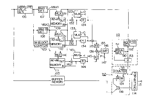
Fig. 17 shows a detailed part of the related
portion with the buffering process of still another
embodiment. An absolute value of an AC coefficient
from the absolute value generating circuit 106 is
supplied to the maximum value detector 107, and a
maximum value MAX1 for each M-block is detected at
the maximum value detector 107. The maximum value
MAX1 is given to a multiplexes 121, and the output
signal of the multiplexes 121 is supplied as a seven-
bit address AO to A6 for the frequency distribution
memory 109. Also, a maximum value MAX2 for each S-
- 4 5 -
block which is detected at the maximum value detector
108 is given to a multiplexes 131, and the output
signal of the multiplexes 131 is supplied as a seven-
bit address AO to A6 for the frequency distribution
memory 110. Further, the absolute value of the AC
coefficient is supplied to a multiplexes 14I, and the
output signal of the multiplexes 141 is given as a
seven-bit address AO to A6 for the frequency
distribution memory 111.
An M-block counter indicated by 120 is
provided, and two bits developed by the counter 120
is supplied to the multiplexers 121, 131 and 141 as
an upper address A7 and A8. The memory area of
memory 109, 110, 111 are divided corresponding to the
M-block by the upper address A7 and A8 respectively.
Data which is read from frequency
distribution memory 109 is supplied to an adder 122
and added to the output of a multiplexes 123 at the
adder 122. Ftere, 0, +1 and the output signal of a
register 124 are supplied to the multiplexes 123, and
one of these input signals is selectively given to
the adder 122. The output signal of the adder 122 is
supplied to a register 124. As has been mentioned
above, the output signal of the register 124 is
feedback to the multiplexes 123 and given to an adder
125.
- 4 6 -
~~~~.~ ~~ r
Data which is read from frequency
distribution memory 110 is supplied to an adder 132
and added to the output of a multiplexes 133 at the
adder 132. Here, 0, +1 and the output signal of a
register 134 are supplied to the multiplexes 133, and
one of these input signals is selectively given to
the adder 132. The output signal of the adder 132 is
supplied to a register 134. As has been mentioned
above, the output signal of the register 134 is
feedback to the multiplexes 133 and given to the
adder 125. The output signal of the adder 125 is
multiplied by 4 through a multiplier 135, and the
output signal of the multiplier 135 is given to an
adder 136.
In association with the frequency
distribution memory 111, an adder 142, a multiplexes
143, a register 144 and a multiplexes (twofold
circuit) 145 are provided like the memory 110. The
multipliers 135 and 145 can be composed of a shift
circuit.
As described later, the number of
transmission bits Q of AC coefficients necessary for
transmission is obtained at the output of an adder
136, and the number of transmission bits Q is supplied
to a comparator 146. An object value P of the number
of transmission bits is given to the comparator 146
_ 4 7 _
from a terminal 147, and detection is made on whether
the calculated transmission bit number Q is larger or
smaller than the object value P. In the case of (P >
Q), the comparison output signal becomes high level,
for example.
The comparison output signal of the
comparator 146 is given to a mode generator 151 of the
control signal generating circuit 113 indicated in a
block by a broken line. The mode generator 151
generates a three-bit mode control signal MD, for
example. The mode control signal MD is supplied to an
address generator 152 and a register 153. The mode
signal generator 151 increases a mode number i from 0
step by step, and watches the comparison output
signal at a stage of each mode number i. When the
realation between the transmission bit number Q and
the object value P is (P > Q), the mode number i is
changed to (i + 1).
The renewal of the mode number i is stopped
when the condition (P > Q) is not satisfied.
To the register 153, the comparison output
signal from the comparator 146 is given as a clock.
When the condition (P > Q) is not satisfied, the mode
control signal MD is taken into the register 153. In
addition, an address signal developed at the address
generator 152 is supplied to the multiplexers 121,
- 4 8 -
a
~J ~ ~ ,e
.~~.~~~t~,~~-
131 and 141, respectively.
Mode i controlled by the mode control signal
MD are as follows, and the number of transmission
bits becomes larger according to the order of the
mode number i:
mode 1: AC coefficient multiplied by 1/64 is
transmitted.
mode 2: AC coefficient multiplied by 1/32 is
transmitted.
mode 3: AC coefficient multiplied by 1/16 is
transmitted.
mode 4: AC coefficient multiplied by 1/8 is
transmitted.
mode 5: AC coefficient multiplied by 1/4 is
transmitted.
mode 6: AC coefficient multiplied by 1/2 is
transmitted.
mode 7: AC coefficient is transmitted as it is.
Here the mode 0 means that the transmission
path overflows with the data even if the transmission
bits number is compressed as large as possible.
However, under the normal condition, such an overflow
does not occur.
The mode control signal MD from the register
153 is supplied to the weighting circuit 112
indicated by a block of a broken line. The weighting
circuit 112 is constituted by a ROM 154 and a
multiplier 156. The ROM 154 is supplied, as an
address, with the mode control signal MD from the
register 153 and an M-block number generated at a
counter 155, and generates a weighting coefficient.
The multiplier 156 for multiplying coefficient data
from the buffer memory 105 and the weighting
coefficient read out of the ROM 154. The output data
of the multiplier 156 is given to the format
development circuit 114 and converted into
transmission data together with the mode control
signal MD.
The supply of the M-block numbar from the
counter 155 at the weighting circuit 112 i.s to make it
possible to perform the multiplication of a finer
weighting coefficient.corresponding to the M-block
rather than a constant weighting coefficient such as
1/2 by the AC coefficient.
With respect to the process to obtain the
transmission bit number, explanation will be given
hereinbelow. The number of L-blocks is indicated by
NB (2700 blocks/field, for example).
First, flag Fm and DC in transmission data
(refer to Fig. 16A) must be transmitted in all blocks
- 5 0 -
independent of contents of a picture. Namely, (4 +
10) X NB = 14NB (37800 bits/field for example) is a
fixed data amount. The bit numbers of the flags F's
and Fp, Ac coefficient data are variable, and it is
necessary to know these bit numbers. At the
comparator 146, a comparison of the data amount Q and
the object value P on the variable bit numbers is
made.
Description will be given on the calculation
of the dada amount of the flag Fs. The case where
the flag Fs must be sent is the case where there is at
least one AC coefficient having a value other than zero
in each 16 samples contained in the M-block Mi.
Therefore, it is sufficient only to focus on the
maximum value MAX1 of the AC coefficients of each M-
block. Now, the frequency distribution of the
maximum value MAXI of the absolute values of the AC
coefficients in the M-blocks Mi of all blocks in one
field is developed, and this frequency distribution
is converted into an accumulated frequency
distribution.
The frequency distribution memory 109 is
cleared before the write-in. The adder 122 generates
zero data at the time of the clear operation. Also,
sequentially changing 9 bits address from the address
generator 152 of the control signal generating circuit
- 5 1 -
~c:fl:~..~.~;~
113 is supplied via the multiplexer 121 to the memory
109, and zero data is written into all addresses (0,
1, 2, ..., 510, 511, for example).
After the clear, the multiplexer 121 selects
the maximum value MAX1 detected at the maximum value
detector 107, and the M-block address. The
multiplexer 123 selects an input of +1. Data at an
address designated by the maximum value MAX1 and the
M-block number is read out of the memory 109 and
added to +1 at the adder 122. The output data of the
adder 122 is written into the same address as input
data of the memory 109. This writing operation is
performed at the rate of once per 16 samples. After
this processing has been done over one field period,
the frequency distribution of the maximum value MAX1
of the absolute values of the AC coefficients is
stored in the frequency distribution memory 109 in
respect of every M-block.
Also, like the frequency distribution memory
109, the frequency distribution memory 110 is cleared
to zero fixst, and the content of the memory 110
added by +1 at the adder 132 is written into the same
address using the maximum value MAX2 of the absolute
value of the AC coefficient detected every S-block
and M-block address as its address so that a frequency
distribution table corresponding to one field period
- 5 2 -
of the maximum value MAX2 is formed into the memory
110 in respect of every M-block. This writing
operation is performed at the rate of once per 4
samples.
Further, like the frequency distribution
memory 110, the frequency distribution memory 111 is
cleared to zero first, and the content of the memory
111 added by +1 at the adder 142 is written into the
same address using the M-block address and the
absolute value of the AC coefficient as its address
so that a frequency distribution table corresponding
to one field period of the absolute value of the AC
coefficients is formed into the memory 111.
If the distribution tables of occurrence
frequency corresponding to one field are formed in
the memories 109, 110 and 111, accumulated frequency
distribution tables are developed from these
frequency distribution tables. For forming an
accumulated frequency distribution table, the
multiplexers 121, 131 and 141 are switched into a
state for selecting the output of the address
generator 152 of the control signal generating
circuit 113, and the multiplexers 123, 133 and 143 are
switched into a state for selecting the respective
outputs of the registers 124, 134 and 144. The
address generator 152 generates the 9-bits address AO
- 5 3 -
2~"~.~.~,~:-
to A8 as mentioned below.
In the duration for forming the accumulated
frequency distribution table of the block M0, the
upper address (A7, A8) is set to (00), and the 7-bits
lower address AO to A6 is generated decrementally such
as (127, 126, 125, ... 2, 1, 0).
In the duration for forming the accumulated
frequency distribution table of the block M1, the
upper address (A7, A8) is set to (10), and the 7-bits
lower address AO to A6 is generated decrementally such
as (127, 126, 125, ... 2, 1, 0).
In the duration for forming the accumulated
frequency distribution table of the block M2, the
upper address (A7, A8) is set to (O1), and the 7-bits
lower address AO to LA6 is generated decrementally
such as (127, 126, 125, ... 2, 1, 0).
In the duration for forming the accumulated
frequency distribution table of the block M3, the
upper address (A7, A8) is set to (11), arid the 7-bits
lower address AO to A6 is generated decrementally such
as (127, 126, 125, ... 2, 1, 0).
A read-out output of each address mentioned
before is added to the outputs of registers 124, 134
and 144 at the adders 122, 132 and 142, respectively.
The registers 124, 134 and 144 are reset at zero
prior to forming an accumulated frequency
- 5 4 -
2~~.~~ ~~'~
distribution table. Therefore, a value from the
address 127 is written into the memories 109, 110 and
111 as an accumulated value with respect to each M-
block. After the addresses of the memories 109, 110
and 111 have changed from the address 127 to the
address 1 every M-block, an accumulated frequency
distribution table is developed in each memory.
The form of the accumulated frequency
distribution table is similar to that shown in Fig. 11
on the whole. Also, since the manner for calculating
the transmission bit number of each flag and the
significant AC coefficients is very similar to the
above-mentioned first embodiment, the detailed
description of that manner is omitted.
Further, after accumulative frequency
distribution table is formed in the frequency
distribution memories 109, 110 and 111, the
multiplexer 121, 131 and 141 are switched into a state
for selecting the address from the address generator
152, and the multiplexer 123, 133 and 143 is switched
into a state for selecting the output signal from the
registers 124, 134 and 144, respectively.
The address generator 152 generate the
address according to a flowchart shown in Fig. 18.
The register 144 is cleared to zero first (a step 161).
Next, the mode number i is set to an initial value (0)
- 5 5 -
~~~~0.~~~
(a step 162). Registers 124 and 134 are cleared to
zero (a step 163). In a step 164 after the step 163,
a value of (64/2') (this value is 64 when i is 0) is
generated as the lower address AO to A6 (a step 164).
The value of (64/2') means a minimum transmission
value ni. The upper address A7 and A8 varies from 0
to 1, from 1 to 2, from 2 to 3, successively (a step
165).
After the upper address A7 and A8 is
advanced from 0 to 3, the output data of the adder
125 indicates the total number of bits of the flag Fs
and Fp per one field as mentioned below. Here j
denotes the number of the M-block.
3
{ 5; (ni) + P; (ni)l
;.o
The output data of the adder 125 is
multiplied by 4 at the multiplier 134, and the output
data of the multiplier 134 is supplied to the adder
136.
With respect to the register 144, the
following output data is obtained, and the output data
is mlutiplied by 2 at the multiplier 145. In the
result, the total number of bits of AC coefficient
data is calculated.
- 5 6 -
~~~~.~.~3~
3
ACJ (ni)
k - 0 J - 0
The comparator 146 compares the amount of
generated data Q with the object value P (a step 166).
When the condition of (P > Q) is satisfied, the mode
number i is changed to (i + 1) (a step 167), and then
the prcocedure returns to the step 163. When the
condition of (P > Q) is broken, the renewal of the
mode number i is stopped (a step 168). The mode
number is decided after the stop, and the mode number
is adopted. The mode control signal MD identifies
the adoped mode number.
As mentioned before, the mode in which the
transmission bit number is smaller than the object
value is decided, and the AC coefficient delayed by
buffer memory 105 is multiplied by the weighting
coefficient corresponding to the above mode.
As described above in detail, the present
invention enables the control so that the data amount
necessary for transmission is smaller than an object
value by the feedforward control. For this reason,
such a problem as oscillation does not occur
differently from the feedback control. In addition,
the invention allows the correct control of the data
- 5 7 -
amount at the unit of one field or one frame and is
suited for a digital VCR. Further, since the amount
of the generated data is calculated for avery M-
block, this invention inables the amount of the
generated data to be controlled finely.
Having described a specific preferred
embodiment of the present invention with reference to
the accompanying drawings, it is to be understood that
the invention is not limited to that precise
embodiment, and that various changes and modifications
may be effected therein by one skilled in the art without
departing from the scope or the spirit of the
invention as defined in the appended claims.
- 5 8 -