Note: Descriptions are shown in the official language in which they were submitted.
-- 2011233
FIELD-EFFECT-TRANSISTOR
WITH ASYMMETRICAL STRUCTURE
The present invention relates generally to
semiconductor devices and more particularly to a field
effect transistor (FET) having asymmetrical source-drain
regions and a method of manufacturing the same.
BACKGROUND OF THE INVENTION
Current efforts towards decreasing the size of
transistor devices have resulted in attempts to fabricate
FETs having increasingly shorter channel lengths. As FET
channels approach the micron and submicron range, however,
the resulting devices exhibit undesirable operating
characteristics. These undesirable characteristics
include, but are not limited to: 1) decreased breakdown
voltage, 2) decreased punch-through voltage, 3) degraded
threshold voltage control, and 4) hot-electron induced
degradation.
Responsive to the above-described problems, various
change~ have been made to the FET structures -
particularly to the source and drain region structures
proximate the device channel. U.S. Patent No. 4,366,613
to Ogura et al., assigned to the asæignee of the present
invention, shows the use of a lightly doped drain (LDD)
~tructure for increasing the breakdown voltage and
inhiblting hot-electron induced degradation in short
channel devices. This LDD structure consists of lightly
FI9-88-031 l
.;.., ., :
-: , : , .. -. . . . . . .... . .. ... . . .
201~233
doped extensions of the source and drain regions, of same
conductivity type as the source and drain regions, into
the channel region.
"A Half-Micron MOSFET Using Double Implanted LDV",
by S. Ogura et al., 1982 IEDM Technical Digest, page 718,
shows an FET including pockets (or "halos") surrounding
the LDD drain and source extensions in the vicinity of the
device channel, these pockets being of opposite
conductivity type to the LDD extensicns. Similar halos
are shown in U.S. Patent No. 4,636,822 to Codella et al.,
assigned to the assignee of the present invention, and in
U.S. Patent No. 4,597,824 to Shinada et al. In operation,
these halos function to reduce undesirable short channel
effects, including decreased threshold voltage and
decreased punch-through voltage.
Japanese Kokai No. 58-194,367 shows an EET including
both LDD source and drain extensions, and a ~ingle pocket
#urrounding the source LDD extension. A process is shown
for forming the device, the process requiring at least one
highly accurate photolithographic masking step.
Japanese Kokai No. 58-115,863 shows an FET including
a buried, high-dopant concentration region underlying the
source and drain region, and at least one pocket
surrounding the drain region, or pockets surrounding both
the source and drain region.
As discussed above, the shortening of the FET
channel~, and the providing of subsequently smaller, more
den~ely packed devices comprises a priority in the field.
FI9-88-031 2
- 2011233
This is evidenced by the above-described publications
directed to just such ends Such accomplishment~,
particularly when achieved without the concomitantly
expected degradations in operating performance, provide a
significant contribution to the art.
OBJECT OF THE INVENTION
An object of the present invention is to provide a new
and improved FET and a method of fabricating the same.
Another object of the present invention is to provide
such a FET having a sub-micron gate length and improved
operating characteristics relative to the prior art.
A further object of the present invention is to
provide a method for fabricating the above-described FET
having a sub-micron gate length and an asymmetrical
structure in the FET channel region.
In accordance with one aspect of the present
invention there is provided a field effect transistor of
asymmetrical structure comprising: a semiconductor
substrate of first conductivity type; source and drain
regions of second conductivity type disposed in a surface
of the substrate and spaced apart by a channel region; and
a single, lightly doped extension of the drain region into
the channel, the extension being of the second
conductivity type and of a lower dopant concentration than
the drain region.
In accordance with another aspect of the invention
there is provided a field effect transistor of
FI9-88-031 3
... . . . . .
.
2011233
asymmetrical structure comprising: a semiconductor
substrate of first conductivity type; source and drain
regions of second conductivity type disposed in a surface
of the substrate and spaced apart by a channel region; a
single halo region generally surrounding the source region
in the substrate, the halo region of the first
conductivity type and of a higher dopant concentration
than the substrate; and a single lightly doped extension
of the drain region into the channel, the extension being
of the second conductivity type and of a lower dopant
concentration than the drain region.
In accordance with another aspect of the invention
there is provided a method of forming a field effect
transistor, comprising the steps of: providing a
semiconductor substrate of first conductivity type;
forming source and drain regions of second conductivity
type in a surface of the substrate and spaced apart by a
channel region; and forming a single, lightly doped
extension of the drain region into the channel, the
extension being of the second conductivity type and of a
lower dopant concentration than the drain region.
In accordance with yet another aspect of the present
invention, there is provided a method of forming a field
effect tran~istor, comprising the steps of: providing a
~emiconductor substrate of first conductivity type;
forming a generally conformal layer of gate electrode
material over the device region; forming a mask over the
layer of gate electrode material, the mask including a
FI9-88-031 4
'
201~2~
generally vertical edge situated over the substrate;
forming a first device region in a portion of the
substrate self-aligned with the mask; using the mask to
define a gate electrode from the layer of gate electrode
material while exposing a previously masked portion of the
substrate adjoining the gate electrode; and forming a
second device region in the newly exposed portion of the
substrate self-aligned with the gate electrode.
:
BRIEF DESCRIPTION OF THE DRAWINGS
These and other objects, features, and advantages of :
the present invention will become apparent from a
consideration of the following detailed description of the .
invention when read in conjunction with the drawing -
Figures, in which:
FIGURE 1 is a cross-sectional view of an in~ulated
gate (IG) FET constructed in accordance with the present
invention;
FIGURES 2A-2F are cross-sectional views showing -
successive steps in a method of constructing the IGFET of
FIG. 1; and
FIGURES 3A-3F are cross-sectional views showing
successive steps in a second method of constructing an
IGFET in accordance with the present invention. -~
DETAILED DESCRIPTION OF THE INVENTION
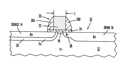
Referring now to the drawings, FIG. 1 shows an IGFÉT
abricated on a ~ub~trate 12 of P- silicon
' . '
FI9-88-031 5 ~ - .
''. -, ' -,
. ,, . .- .
'' ' '' "' , ; :' ' ,
20~ 233
semiconductor material. As used herein, "P" and "N" refer
to semiconductor doping types, while "+" and "-" are used
as appropriate to describe relative doping concentrations.
IGFET 10 includes heavily doped N+ source and drain
regions, 14 and 16, respectively, disposed in the surface
of substrate 12 and spaced by a channel portion 18 of the
substrate. A gate structure 20 is situated on the surface
of substrate 12, generally spanning source and drain
regions 14, 16, and overlying channel region 18. Gate
structure 20 includes an electrode 22 of conductive
material, preferably doped polysilicon or a metal such as
an aluminum-copper alloy, the electrode being spaced from
the surface of substrate 12 by a thin layer 24 of silicon
dioxide (SiO2). Gate electrode 22 is of a length L, as
described in further detail below, that may beneficially
be shorter than 1 micron. Channel region 18 can include
a threshold adjustment implant (not shown) in a manner
well understood in the art.
In the embodiment shown, gate structure 20 further
includes sidewalls 26A, 26B of an insulating material,
preferably silicon nitride (Si3N4). Sidewalls 24A, 24B
are used both in the formation of the device source and
drain regions in the manner described below, and as
in~ulators in the subsequent metallization ~not shown) of
IGFET 10.
In accordance with one aspect of the present
invention, IGFET 10 includes further structural features
making the device asymmetrical proximate channel region
FI9-88-031 6
.
- 2~1~233
18 underneath gate structure 20. More specifically, an
N-, lightly doped extension (or tip) region 28 extend~
from the edge of N+ drain region 16, underneath sidewall
26B and just past the right-most edge of gate electrode
22. Extension 28 is of a lower dopant concentration and
lesser depth into substrate 12 than is drain region 16.
It is an important feature of the present invention that
extension 28 is formed only on drain region 16, and not
symmetrically on source region 14 as is commonly taught
in the art.
A further important feature of the present invention
is the inclusion of a single P+ halo, or pocket region 30
extending from channel 18 beneath gate electrode 22 and
surrounding source region 14. Again, it is important to
note that IGFET 10 includes only the single halo 30
surrounding the source region 14, and no symmetrical halo
surrounding drain region 16 as is taught conventionally
in the art.
In operation, extension region 28 of drain 16
functions to increase the device breakdown voltage and
reduce the hot carrier effects, while the exclusion of the
~ymmetrical extension from the source region avoids a high
series resistance and accompanying drawbacks associated
therewith. Additionally, it has been discovered that the
inclu~ion of halo region 30 about source region 14
function~ to reduce short channel threshold voltage
fall-off, and also to inhibit device punch-through.
Becau#e no halo i~ formed ~urrounding drain region 16, the
FI9-88-031 7
201~233
present invention avoids disadvantages of decreased
breakdown voltage and increased device capacitance
associated therewith.
Analysis of IGFET 10 as described above shows that
the device can be operated with a channel length L in the
range of 0.10-0.20, microns while exhibiting greatly
improved operating characteristics relative to prior art
devices attempting to achieve this same dimension.
It will be noted at this point that, while IGFET 10
has been described as including two asymmetrical features,
i.e. halo 30 about source 14 and extension 28 with drain
16, either of these features may be utilized singly to
improve the operating characteristics of the devices.
Further, while the invention has so far been described
with respect to an N-channel, enhancement mode device,
through the appropriate adjustment of conductivity types
and concentrations, it is equally applicable to P-channel
enhancement mode devices, and to both N- and P-channel
depletion mode devices.
Referring now to the series of FIGS. 2A-2E, a method
of forming an asymmetrical FET device of the type shown
in FIG. 1 is illustrated and described. It is noted at
this point that the formation of IGFET 10 with a
sub-micron channel length L requires extremely accurate
alignment of the various device regions and structures.
Thi~ accuracy is not typically available using
conventional photolithographic techniques.
FI9-88-031 8
2011233
Referring now to FIG. 2A, a portion 40 of a P-,
silicon semiconductor substrate is provided for supporting
the formation of an FET device. A layer 42 of oxide
(SiO2) is formed over the upper surface of substrate 40,
layer 42 including a relatively thin gate oxide region 42A
bounded by relatively thicker, electrically isolating
field oxide regions 42B, 42C. Oxide layer 42 is formed
by known, conventional techniques. Gate oxide region 42A
has a thickness, for example, in the range of about
100-200 Angstroms.
A layer 44 of polysilicon is formed over oxide layer
42, for example to a thickness of about 3,000 Angstroms.
Polysilicon layer 44 can be formed by a conventional
chemical vapor deposition (CVD) process, and is either
formed in situ doped, or subsequently doped by ion
implantation (I/I) to a concentration in the range of -
about lx102 atoms/cm3. A thin layer 46 of SiO , for -
example in the range of 400 Angstroms, i5 formed on the ----
upper surface of polysilicon layer 44. Oxide layer 46 can
be formed, for example, by a conventional process of
thermal oxidation or chemical vapor deposition. ~-
Continuing to describe FIG. 2A, a mask 48 of
photoresist material is formed so as to include a
substantially vertical edge 48A generally centered over
the surface of gate oxide region 42A. Mask 48 is formed
using conventional photolithographic techniques of
blanket deposition of a photoresist material (a single or
multilayer photoresist structure can be used), and
FI9-88-031 9
' ' ', ,'' ,' -' ' ' ' ' ' ," ' ' ''. , ',' ' ~' ',, ' , ', '' ', ,'" '', " ,', ' ,- ' ' '
-- 2~11233
exposure and development of the regist to form the mask.
It should be noted that the positioning of edge 48A, a
step not critical to the subsequent formation of a FET
device, is the only step in the device formation which is
not self-aligned to other device features.
Subsequent to the formation of mask 48, a vertical
sidewall 50 of insulating material, preferably plasma
deposited Si3 N4, is formed over edge 48A. Sidewall 50 is
formed, for example by a conventional process including
the steps of: l) forming a layer of Si3 N 4 generally
conformally over the surface of the device, and 2) etching
the Si 3N4 layer with an anisotropic etch process to leave
sidewall 50. An appropriate etch process would include a
reactive ion etch (RIE) with a plasma selective to Si3N4,
for example CHF3 or CF4/H2. The thickness, Tl, of sidewall
50 can be very accurately controlled by controlling the
thickness of the conformal layer of Si 3N4.
To obtain the structure shown in FIG. 2B, the exposed
portions of oxide layer 46 and the subsequently exposed
portions of underlying polysilicon layer 44 are
sequentially removed. It is desired to leave vertical
edges subsequent to the removal of these layer portions,
and hence the use of an anisotropic RIE process is
preferred. Exposed portions of oxide layer 46 are
removed, for example, using a RIE process with a CF4
plasma. Subsequently exposed portions of polysilicon
layer 44 are then removed, for example, using a RIE
FI9-88-031 10
, " :,: ,, , : ,
,, ' , ,, ~, :, . .. . . ..
20~233
process with a C12 plasma. This Cl2 plasma is effectively
stopped by oxide layer 42.
P+ ions (not shown) are implanted into the portion
of substrate 40 framed between field oxide region 42B and
sidewall 50, using the field oxide, sidewall, and mask 48
as the I/I mask. This I/I is performed, for example,
using boron ions, and with a power and dopant
concentration sufficient to form a P~ halo region 52 to a
depth greater than a subsequently formed source region.
A second I/I is then performed with N~ ions, for example
of phosphorus or arsenic, to form an N+ source region 54
within halo region 52. This second I/I uses the same mask
as that used to form halo region 52. It will be
understood that the relative order of forming the~e halo
and source regions can be reversed.
- A protective layer 60 of SiO2 is deposited
conformally over the device, to a thickness of about 800
Angstroms.
To form the structure of FIG. 2C, a planarized layer
61 of resist material is formed over those portions of the
device not covered by mask 48. Resist layer 61 is formed
by the conventional process of spinning on a layer (not
#hown) of resist to a thickness greater than that of mask
48. A~ i~ known in the art, this spinning process results
a resist layer having a relatively planar upper surface.
Thi~ relatively planar layer of resist is then thinned,
for example using a RIE process with an oxygen plasma, to
a thickne~s slightly less than that of mask 48. Thi~
FI9-88-031 11
.
2011233
thinning process results in the higher regions of oxide
layer 60 (i.e. those regions covering the upper surface
of mask 48 and sidewall 50) being exposed.
To obtain the structure shown in FIG. 2D, appropriate
etchants are used to remove first the exposed regions of
oxide layer 60, and next the resist materials including
layer 61 and mask 48. For example, an HF solution can be
used to remove the exposed portions of oxide layer 60,
while an oxygen plasma can be used to remove the resist
materials. The resulting device includes a narrow,
vertical structure 64, defined by sidewall 50 and the
adjoining vertical portion 65 of oxide layer 60.
To form the structure shown in FIG. 2E, nitride
sidewall 50 is used as a mask for a directional etch of
first the exposed region of oxide layer 46, then the
exposed region of polysilicon layer 44. Oxide layer 46
can be etched, for example, using a RIE process with a
CF4 plasma, which will also reduce the thickness of oxide
layer 60. Polysilicon layer 44 can be etched, for
example, with a RIE process using a Cl2 plasma. Sidewall
50 is then removed using an appropriate etch, such as
H3PO4. The remaining, freestanding vertical portion 65
of oxide layer 60 is removed using a mild, 50:1 solution :
of HF. Because vertical extension 65 of oxide layer 60 ~ -
i8 freestanding, the HF solution will etch the extension --
bi-directionally, removing the extension while leaving a ` -
thickness of the remaining portion of layer 60. The
FI9-88-031 12
," , ~, . , , " . . . .
,:, . ., :,: . ,,, :. ' ,: ' ,. ' ,
-` 2011 233
result of these etching steps is the definition of a
polysilicon gate electrode 62.
An I/I is performed in the surface of substrate 12,
so as to form a relatively shallow, relatively lightly
doped N- region 64 extending between gate electrode 62 and
field oxide region 42C. This I/I is performed using field
oxide regions 42B, 42C, and gate electrode 62 as an I/I
mask. It will be appreciated that this relatively light,
shallow I/I has no appreciable affect on the heavily doped
source region 54 or the heavily doped, deeper halo region
52.
Referring now to FIG. 2F, sidewalls 66A, 66B of
insulating material, preferably SiO2, are formed on the
vertical edges of gate electrode 62. Sidewalls 66A, 66B
are formed by a conventional proces~ of blanket depositing
a thick layer of oxide (not shown) conformally over the
device, then anisotropically etching the thick layer with
an appropriate RIE process, for example using a CHF3
plasma. The thickness T2 of sidewalls 66A, 66B can be
very accurately controlled by controlling the thickness
of the conformal layer of oxide. -
Subsequent to the formation of sidewalls 66A, 66B,
an I/I of N~ ions is performed, for example using arsenic,
80 as to form a drain region 68 in substrate 12 between ~-- - -
sidewall 66B and field oxide 42C. The power and dopant
concentration of the I/I are selected so as to make drain -~-
region 68 relatively deeper and more highly doped than
lightly doped extension 64. Sidewalls 66A, 66B, and field
FI9-88-031 13
- 2~11233
oxide regions 42B, 42C, function as masks for this I/I.
It will be appreciated that the device area over source
region 54 is left unmasked, this last I/I functioning
beneficially to increase the concentration of the source
region. The remaining exposed portions of oxide layers
46, 60 are subsequently stripped by an appropriate
etchant, for example a 40:1 HF solution, to leave the
structure shown in FIG. 2F.
The resultantly formed enhancement-mode, N channel
IGFET 68 is identical to device 10 of FIG. l above.
Through a consideration of the above-described
process steps, it will be appreciated that, by using
sidewall 50 as a mask in forming halo region 52 and source
region 54 (FIG. 2A), these two regions are self-aligned
with each other and with subsequently defined gate
electrode 62. In a similar manner, by using gate
electrode 62 as a mask in forming lightly- doped extension
region 64 (FIG. 2E), the extension region is self-aligned
to the gate electrode. The use of sidewall 66B as a mask
to form drain region 68 (FIG. 2F) makes the drain region
self-aligned relative to both gate electrode 62 and
extension region 64.
These self-aligned process steps comprise major
features of the present invention, and provide the
significant advantage of permitting the FET to be reliably
and repeatedly formed with a channel length L of
~ub-micron dimen~ion as described above. They further
permit these accurate dimensions to be achieved while
FI9-88-031 14
2~1~233
simultaneously providing an asymmetrical device having the
improved operating characteristics as described with
respect to FIG. 1 above.
Referring now to the series of FIGS. 3A-3D, a
modified embodiment of the process of FIGS. 2A-2F is shown
wherein it is desired to form the asymmetrical halo region
52 around source region 54. Like features are indicated
by like reference numbers.
Referring now to FIG. 3A, a device structure
substantially identical to that of FIG. 2A above is shown,
one difference being that P+ halo region 52 has been
implanted prior to the etching of layers 44 or 46 so as
to be self-aligned to sidewall 50. The only other
difference is the inclusion of an optional, CVD deposited
layer 47 of polysilicon over oxide layer 46.
FIG. 3B shows resist mask 48 removed, while FIG. 3C
is obtained by using sidewall S0 as a mask to etch the
exposed portions of layers 47, 46, sequentially, and then
removing the sidewall itself. These features are etched
using appropriate processes as described above. It will
be appreciated that polysilicon layer 47, which can also
be used in the process of FIGS. 2A-2F described above,
functions as an etch stop during the removal of resist
mask 48.
To obtain the structure shown in FIG. 3D, the
remaining, registered portions of layers 46, 47 are used
a~ a mask in an anisotropic RIE process to remove the
exposed portions of polysilicon layer 44. It will be
FI9-88-031 15
, . . . .
- 2011233
understood that polysilicon layer portion 47 is also
removed in this last etching step. This etching step is
performed using the appropriate etch process described
above, and results in the definition of gate electrode 62.
A portion of oxide layer 46 remains on the upper surface
of the gate electrode.
To obtain the structure of FIG. 3D, field oxide
regions 42B, 42C, and gate electrode 62 with oxide cover
46, are used as a mask for an I/I. This I/I is performed
with N+ ions to form highly doped N+ source and drain
regions 54, 68, respectively. This I/I is performed such
that source region 54 is relatively shallower than halo
region 52. It will be appreciated that halo region 52 is
self aligned to source region 54, and that the halo,
source, and drain regions are all self-aligned to gate
electrode 62.
To complete the desired FET structure, a layer 66
(shown in FIG. 3E) is formed conformally over the device,
and subsequently etched to leave the FET structure 70
shown in FIG. 3F. FET 70 of FIG. 3E is substantially
identical to FET 68 of FIG. 2F, with the exclusion of the
LDD extension 64 included in the latter.
From a consideration of the above-described process
steps, it will be appreciated that the processes of FIGS.
series 2 and 3 each describe a method of fabricating an
FET device wherein source and drain regions are
~elf-aligned to a gate structure. The processes are
capable of reliably and repeatedly forming FETs having
FI9-88-031 16
2011233
sub-micron gate lengths, and can advantageously be used
to form devices of asymmetrical structure.
There is thus provided a new and improved FET having
a sub-micron channel length and exhibiting significantly
improved operating characteristics relative to prior art
devices. This operation is obtained through the use of
an asymmetrical source and/or drain structure in the
region of the device channel. Further provided is a new
and improved method for forming a FET having the device
source and drain regions self-aligned to the device gate.
This process is particularly adaptable for use in the
manufacture of an asymmetrical FET.
The present invention has application in the
manufacture of semiconductor devices, and particular
application in the manufacture of very large scale
integration (VLSI) logic and memory circuits including
IGFET devices.
While the present invention has been shown and
described with respect to preferred embodiments, it will
be appreciated that it is not so limited. Numerous
modifications, changes and improvements will occur to
those skilled in the art without departing from the spirit
and scope of the invention.
FI9-88-031 17