Note: Descriptions are shown in the official language in which they were submitted.
2011~02
EN9-89-008
BUS - T0 - BUS ADAPTER
Technical Field
This invention relates to bus-to-bus adapters for
coupling two different data processors to one another so
that data can be transferred from one processor to the other
and vice versa. This invention is particularly useful for
the case where the two data processors are constructed in
accordance with two substantially different computer
architectures.
Backqround of the Invention
In data interfaces between two data processors, it is
known to employ a buffer storage mechanism for purposes of
buffering the flow of data from one processor to the other
and vice versa. A block of data to be transferred is moved
from one processor and stored into the buffer ctorage
mechanism. Thereafter, this block of data is read out of
the buffer storage mechanism and transferred to the second
data processor. These transfers into and out of the buffer
storage mechanism cannot occur simultaneously because all of
the arriving data must be present in the buffer storage
before the buffer emptying process can begin.
Processor-to-processor data transfer methods which employ
this buffer storage technique are sometimes referred to as
"store and forward" methods or "mailbox" methods. ~
2 ~ 0 2
EN9-89-008 2
While the known methods are generally satisfactory,
there is nevertheless room for improvement. In particular,
it is desirable to provide processor-to-processor interfaces
which enable faster data transfer rates between the two
processors. It is further desirable to provide now and
improved interface mechanisms which enables multiple
independent processor-to-processor operations to occur in a
concurrent manner.
Summary of the Invention
In accordance with the present invention, there is
provided a new and improved bus-to-bus adapter unit for
coupling the input/output (I/0) bus of a first data
processor to the input/output (I/0) of a second data
processor for enabling fast and efficient transfers of
messages and data from one processor to the other. This
bus-to-bus a apter includes a buffer storage mechanism for
temporarily storing the data during its passage from one
processor to the other. A control mechanism is provided for
enabling multiple independent data buffer areas to be
established in the buffer storage for enabling multiple
independent processor-to-processor storage operations to
occur concurrently with one another. These transfer
operations need not be in the same direction. Some may move
data from the first processor to the second, while others
may move data in the opposite direction. This multiple
buffer technique increases the data transfer flexibility
where different types of data sources are associated with
one or both of the processors.
2 ~ 0 2
EN9-89-008 3
Another feature of this new bus-to-bus adapter is the
provision of a mechanism for enabling different amounts of
service time to be allocated to different ones of plural
independent but concurrent transfer operations. This
enables higher priority transfer operations to be processed
at faster rates than lower priority transfer operations.
This new and improved bus-to-bus adapter also includes
a mechanism for enabling data retrieval from a particular
buffer storage area to begin before all incoming data for
that buffer storage area has been received by the buffer.
This overlaps the transfer in and the transfer out of data
from this given buffer storage area. This increases the
rate at which data can be transferred from one processor to
the other.
A processor-to-processor interace adapter constructed
in accordance with the present invention is particularly
useful for the case where the two processors and their I/0
busse~ are constructed in accordance with two substantially
different and basically incompatible computer architectures.
For a better understanding of the present invention,
together with other and further advantages and features
thereof, reference is made to the following description
taken in connection with the accompanying drawings, the
scope of the invention being pointed out in the appended
claims.
2 ~ 0 2
... , , ,.,, .. ~
EN9-89-008 4
Brief Description of the Drawings
Referring to the drawings:
Fig. 1 shows a general block diagram of a two processor
data processing system including a bus-to-bus adapter
constructed in accordance with the present invention;
Fig. 2 is a storage map for the buffer storage unit
used in the bus-to-bus adapter of Fig. l;
Fig. 3 shows in greater detail the contents of the down
message control block of Fig. 2;
Fig. 4 shows in greater detail the contents of the up
message control block of Fig. 2;
Fig. 5 shows in greater detail the contents of the data
transfer control block #l of Fig. 2;
Fia. 6 is a partial storage map for the buffer storage
unit of Fig. 2 and illustrates the establishment of multiple
independent data buffer areas in the buffer storage unit;
Fig. 7 is a block diagram showing the interrelationship
of various sequencer mechanisms used in the adapter control
unit of Fig. l;
Fig. 8 is a flow diagram showing the order in which the
different message and data transfer areas in the buffer
storage unit are serviced;
Fig. 9 is a block diagram showing in greater detail the
internal con~truction of the adapter control unit of Fig. l;
Fig. 10 is a block diagram showing in greater detail
the internal construction of the count and address counters
of Fig. 9; and
:'
2 ~ 0 2
EN9-89-008 5
Fig. 11 shows in greater detail the internal
construction of the data tranæfer control logic of Fig. 9.
2 ~ 0 2
EN9-89-008 6
Deæcription of the Preferred Embodiment
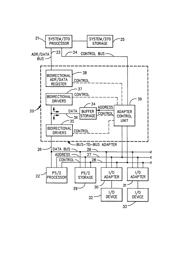
Reerring to Fig. 1, there is shown a bus-to-bus
adapter 20 for coupling the input/output (I/O) bus of a
first data processor 21 to the input/output (I/O) bus of a
second data processor 22. The first data processor 21 may
be, for example, an IBM** type System/370* processor. A
detailed description of the architecture and machine
functions provided by a System/370 processor are described
in a technical manual entitled "IBM System/370 Principles of
Operation", Eleventh Edition (Sept. 1987), published by IBM
Corporation of Armonk NY, IBM Order No. GA22-7000. The
second data processor 22 may be, for example, an IBM type
Personal System/2** (PS/2)** Model 80 processor. Such
processor is described in a technical publication entitled
"Personal System/2 Model 80 Technical Reference", published
by IBM-Corporation of Armonk NY, IBM Order No. S68X-2256.
The I/O bus for the System/370 processor 21 includes a
multi-line address/data bus 23 and a multi-line control bus
24. A System/370 storage unit 25 is connected to the
System/370 processor 21.
The I/O bus for the Personal System/2 (PS/2) processor
22 includes a multi-line data bus 26, a multi-line address
bus 27 and a multi-line control bus 28. A PS/2 storage unit
29 is connected to this I/O bus. Various peripheral units
or I/O units are also coupled to the PS/2 I/O bus 26-28.
** Registered Trade Mark
* Trade Mark
2011~02
EN9-89-008 7
For example, first and second I/O adapters 30 and 31 are
coupled to this PS/2 bus 26-28. I/O devices 32 and 33 are
are coupled to respective ones of the I/O adapters 30 and
31.
The bus-to-bus adapter 20 includes a buffer storage
unit 34 for storing data supplied by either one of the data
processors 21 and 22 and for transferring such data to the
other one of the data processors 21 and 22. The data flow
path from the PS/2 processor 22 to the buffer storage 34 is
by way of PS/2 data bus 26, bidirectional drivers 35, and
buffer data bus 36. The data transfer path between the
buffer storage 34 and the System 370 processor 21 is
provided by buffer data bus 36, bidirectional drivers 37,
bidirectional address/data register 38 and the System 370
address/data bus 23. Both of these data flow paths are
bidirectional in nature. Data and messages may flow from
the System 370 processor 21 to the buffer storage 34 or vice
versa. Similarly, data and messages may flow from the PS/2
processor 22 to the buffer storage 34 or vice versa.
Data or messages are never allowed to flow directly
from the System/370 processor 21 to the PS/2 processor 22 or
vice versa. All and all messages data must first be stored
in the buffer storage 34 and then read out and supplied to
the second processor. The two sets of bidirectional drivers
and 37 are never both active at the same time. If
bidirectional drivers 35 are turned on for data transfer
purposes, then bidirectional drivers 37 are turned off and
via versa.
One reason for using the buffer storage 34 as an
intermediary is the fact that the System 370 I/O bus 23-24
2011~02
EN9-89-008 8
has a considerably different architecture from the PS/2 I/0
bus 26-28. They have different numbers of data lines,
different operating cycle requirements, etc. Thus, it is
necessary to reformat or reorganize the data before sending
it on to the next data processor.
The bus-to-bus adapter 20 alæo includes an adapter
control unit 39 for controlling the operation of the other
units in the adapter 20. The adapter control unit 39
controls, for example, the addressing and read verses write
(R/W) status of the buffer storage 34. It also controls the
operational status and flow direction of the bidirectional
drivers 35 and 36 and the address/data register 38. The
adapter control unit 39 receives appropriate control signals
from the System/370 processor 21 via control bus 24 and from
the PS/2 processor 22 via its control bus 28. It also
receives address information from the PS/2 processor 22 via
its address bus 27.
~ ig. 2 shows a storage map for the buffer storage 34.
The buffer storage 34 is organized into addressable lines of
data (words of data), each line containing four bytes. The
lowest address (zero) is at the top of the map and the
highest address is at the bottom of the map. The lower most
address range of the buffer storage 34 is dedicated for use
by a set of relatively small control blocks indicated at
40-45. Each control block area has a few lines or words of
storage capacity. The remainder of the buffer storage 34 is
comprised of a relatively large data buffer area 46 for
temporarily storing the data being transferred. This data
buffer area 46 may have a capacity of, for example, 32
kilobytes (8,000 words).
,.~ .
2011~2
EN9-89-008 9
In the present embodiment, the word "down" is used to
denote the overall direction of movement for data or
messages being moved from the System 370 processor 21 to the
PS/2 processor 22. The word "up" is used to refer to the
general direction of movement for data and messages
transferred from the PS/2 processor 22 to the System 370
processor 21. The down message and the up message control
blocks 40 and 41 enable messages to move in only the down
direction or the up direction, respectively. Each of the
data transfer control blocks (DTCB s) 42-44 is bidirectional
.,., . ,., ., ,~
in nature. Each is capable of controlling the movement of
data in either the down direction or the up direction.
Figs. 3, 4 and 5 show the format or layout for the
information that can be loaded into the control blocks 40,
41 and 42, respectively. As seen 60me portions of these
control block areas are not used or more precisely have not
been defined for use. Also, those that have been defined
for use (by the presence of a label) are not always used in
all cases. The remaining data transfer control blocks 43-45
each have the same format as shown in Fig. 5 for the first
data transfer control block 42.
The various data transfer control blocks 42-45 are used
to establish and manage separate and independent data buffer
areas in the large data buffer area 46 of Fig. 2. The
manner in which this is done is illustrated in Fig. 6 for
the case of the first two data transfer control blocks 42
and 43. As there seen the first data transfer control block
42 establishes a first data buffer area 48 and the second
data transfer control block 43 establishes a separate and
different data buffer area 49. The beginning address for
2011~02
EN9-89-008 10
the first data buffer area 48 is defined by the data buffer
begin address contained in the first two bytes of the last
word of the first data transfer control block 42. The
ending address for the first data buffer area 48 is defined
by the data buffer end address value contained in the last
two bytes of the last word of the control block 42. In a
similar manner, the begin address and end address values in
the second data transfer control block 43 define the
starting and ending addresses for the second data buffer
area 49.
The separate data buffers defined by the various data
transfer control blocks may be used for separate and
independent processor-to-processor data transfer operations.
Thus, for example, the first data buffer 48 may be used for
transferring printing data from the System 370 processor 21
to a printer coupled to the PS/2 I/0 bus 26-28. At the same
time, the second data buffer 49 may be used for transferring
data from a disk storage unit coupled to the PS/2 I/0 bus
26-28 to the System/370 processor 21 for storage in its
storage unit 25. As will be seen, these two different data
transfer operations may be performed in a concurrent manner.
It should be noted that all four of the DTCB defined
data buffers need not be used during any given period of
time. In other words, in any given period, one or more of
the data transfer control blocks may not be in use and may
not contain any valid information. When any given data
transfer control block is not in use, it will not in effect
have any data buffer area associated with it. When a data
transfer control block is first initialized for U#e, it may
be provided with a data buffer area in any unused portion of
2011~02
EN9-89-008 ll
the total data buffer area 46 and its size may be any size
within reason, that is permitted by the then unallocated
portion of the total data buffer 46. Thus, this multiple
data transfer buffer arrangement is quite flexible in
nature. Also, the present invention is not limited to use
of only four data transfer buffers. A greater or lesser
number may be used, as conditions may require.
The down message control block 40 and the up message
control block 41 shown in Fig. 2 do not establish any data
buffer areas in the large data buffer area 46. The
information to be transferred is contained in the down
message or up message control block itself. If need be, the
down message and up message control blocks can be redefined
to include one or more additional words.
The adapter control unit 39 of the bus-to-bus adapter
20 of Fig. l includes a set of five hard-wired sequencers
for individually controlling different phases of the message
and data transfer operations. These sequencers are shown in
Fig. 7. A main sequencer 50 selects which one of the
following three sequencers is operational at any given
moment: an up message sequencer 51; a down message sequencer
52; and a System/370 data transfer sequencer 53. Only one
of these three sequencers 51, 52 and 53 can be operational
at any given moment.
When operational, the up message sequencer 51 functions
to control the buffer storage 34, the bidirectional drivers
37 and the bidirectional address/data register 38 to cause
the up message control block 41 to be transferred from the
buffer storage 34 to the System/370 processor 21. When
operational the down message sequencer 52, on the other
2011~2
EN9-89-008 12
hand, serves to transfer a down message (the information
contained in the down message control block 40) from the
System/370 processor 21 to the down meS#age control block in
the storage buffer 34 When active, the System/370 data
transfer sequencer 53 operates to transfer a packet of data
from the buffer storage 34 to the System/370 processor 21 or
vice versa, such data packet being read from or written into
the large data buffer area 46.
Each of the sequencers 51-53 normally operates in
conjunction with a System/370 bus sequencure 54 and a buffer
sequencure 55. The System/370 bus sequencer 54 controls the
flow direction through and the loading of data into the
bidirectional address/data register 38. It also does the
signal transfer h~n~sh~king with the System/370 processor 21
and controls the multiplexing and demultiplexing which is
required where the address/data bus 23 has a different
number of lines than the buffer data bus 36.
The buffer sequencer 55 controls the selective
activitation and the flow directions for the bidirectional
drivers 35 and 37. This controls the toggling of the buffer
data bus 36 between the PS/2 and the System/370 data flow
paths. The buffer sequencer 55 also selects the address
source and the read/write control source for the buffer
storage 34.
T~e main sequencer 50 selectively of the -
activates, one at a time, the up message sequencer 51 the
down message sequencer 52 and the System/370 data transfer
sequencer 53. Main sequencer 50 provides the allocation
mechanism which determines how often and how long each of
the sequencers 51-53 is activated. The allocation algorithm
20il502
EN9-89-008 13
used in the present embodiment also makes use of a data
transfer repeat counter 56 and a comparator 57. The repeat
counter 56 is programmable and determines how many packets
of data are transferred for each data transfer control block
session. For each such session, this counter is initially
loaded with the number of packets to be transferred and is
decremented by a factor of one each time a packet is
-transferred. The comparator 57 provides an output control
signal which indicates that the count R in the repeat
counter 56 is greater than zero. This tells the main
sequencer 50 that there are more packets to be transferred
for the control block session which is then taken place.
Fig. 8 is a flow diagram showing the service time
allocation algorithm implemented in the main seguencer 50.
The basic service allocation routine is to service the up
message control block 41 and the data transfer control
blocks 42-45 one at a time in a round robin fashion, with
this basic loop being completed by the flow path 58. The
basic routine is for each of the data transfer control
blocks to transfer one packet of data each time it is
serviced. This can be modified by loading a nonzero count
value into the repeat counter 56 of Fig, 7 as one or more of
the data transfer control blocks comes up for service. The
decision block R 0 appearing at the output of the data
transfer control block 42, for example, means that the main
sequencer 50 looks at the output of the comparator 57 and
asks the question as to whether the repeat counter 56
contains a nonzero value. If the answer is yes, then the
feedback path 59 is taken and the data transfer control
block 42 is serviced one more time to transfer one more
2011~02
EN9-89-008 14
packet of data. If the answer is no, then service is passed
to the next data transfer control block 43. Each of the
remaining data transfer control blocks 43-45 has the same
kind of repeat feedback mechanism. Thus, depending on the
repeat count values loaded into repeat counter 56, one or
more of the data transfer control blocks 42-45 can be caused
to transfer more than one data packet during its data
tran~fer session.
If any of the control blocks 41-45 is inactive when its
turn comes up, then control is immediately passed to the
next control block in the chain. Each control block
contains a status bit which indicates whether or not such
control block is active. These status bits are examined by
the main sequencer 50 to determine whether or not to move on
to the next control block.
The down message control block 40 is given special
priority status. It is taken up out of turn and is
immediately serviced whenever it becomes active. More
precisely, it is serviced just as soon as the currently
executing control block plus its repeats gets finished. This
is one before going to the next control block in the primary
chain. For the case of a data transfer control block which
is programmed to transfer more than one packet, the down
message control block 40 must wait until after all packets
have been transferred before being serviced.
The main seguencer 50 also includes a mechanism for
phasing in requests for data transfers between the buffer
storage 34 and the PS/2 processor 22. In particular, a PS/2
data transfer request signal 60 is supplied to the main
sequencer 50 and such sequencer treats it as a priority
2 ~ 0 2
EN9-89-008 15
request. Such request is serviced intermediate the then
executing the control block and the next control block in
the main chain. A PS/2 request will not, however, break
into a repeat count operation being performed by a data
transfer control block. When a PS/2 request is being
honored, the main sequencer 50 temporarily suspends further
operation of the up message, down message and data transfer
sequencers 51-53.
Each of the sequencers 51-55 is a hard-wired state
machine. Each of these sequencures is like a small
dedicated special purpoæe computer or controller having a
hard-wired control program, as opposed to a software or
microcode control program. For this reason, faster
operation is obtained than could be obtained by using a
microprocessor.
The bus-to-bus adapter 20 is completely compatible with
the standard System/370 I/O protocol. As is known,
System/370 I/0 operations are initiated when the application
program or the operating system program in the System/370
storage unit 25 issues a "START I/0" instruction. The
occurrence of such an instruction causes the System/370
processor 21 to send a channel address word (CAW) to an I/O
unit which, in this case, is represented by the PS/2
processor 22. This channel address word is sent to the PS/2
processor 22 by means of a down message control block which,
among other things, includes the System/370 storage address
of the I/0 command to be executed.
In response to this CAW, the PS/2 processor 22
commences to fetch the System/370 channel command word (CCW)
from the System/370 storage unit 25. This is accomplished
201~02
EN9-89-008 16
by means of a data transfer control block and it's
associated data buffer area. In particular, the PS/2
processor 22 initializes a data transfer control block and
places the System/370 storage address for the CCW in the
data address field of such control block. This data
transfer control block then fetches the two CCW words from
the System/370 storage unit 25. These CCW or channel
command words contain the command code, the starting
System/370 data address and the byte count, which byte count
designates the number of data bytes to be transferred for
this System/370 I/0 operation.
The PS/2 processor 22 uses this CCW information to set
up a data transfer control block for doing the
processor-to-processor data transfer operation specified by
the CCW. This processor-to-processor operation may be in
either direc'ion. If it is a System/370 data fetch
operation, then the requested data is transferred from the
System/370 storage unit 25 to the PS/2 storage unit 29. If,
on the other hand, it is a System/370 store operation, then
data is transferred from the PS/2 storage unit 29 to the
System/370 storage unit 25.
After completion of a System/370 I/0 operation, the
PS/2 processor 22 sends a condition code or status message
to the System/370 processor 21 advising it of the status of
thinqs at the end of the I/0 operation. This is
accomplished by way of an up message control block.
Referring to Fig. 9, there is shown in greater detail a
portion of the hardware contained within the adapter control
unit 39 of Fig. 1. As seen in Eig. 9, the adapter control
unit 39 include~ an address register 62 for supplying to
2 0 ~ 2
EN9-89-008 17
buffer storage 34 the address of the word to be accessed.
This buffer address may be obtained from anyone of various
sources. The source selected at any given moment is
controlled by a multiplexer 63. One of the selectable
addresses supplied to the multiplexer 63 is the PS/2 address
appearing on the PS/2 address bus 27. This address is used
when data is being transferred from the PS/2 processor 22 to
the buffer storage 34 or vice versa. Another address source
connected to the multiplexer 63 is count and address
counters 64. As will be seen in connection with Fig. 10
this count and address counter unit 64 includes a buffer
address counter mechanism which is used when transferring
data from the buffer storage 34 to the System/370 processor
or vice versa.
A further address source is setup logic 65. Setup
logic 65 is used for addressing the buffer storage 34 for
purposes of initializing the count and address counters in
unit 64 at the beginning of each data transfer control block
operation. This initial setup routine includes the reading
of the data buffer begin address, the byte count value and
the System/370 data address contained in the data transfer
control block and the placing of such values into the
appropriate address and count registers in the count and
address counter unit 64. These values are transferred to
the uni t 64 by way of the bus 66 which is connected to the
buffer data bus 36. This mechanism is also used for storing
status and update values back into the data transfer control
block at the end of the current data transfer control block
session.
2011~2
EN9-89-008 18
The adapter control unit 39 also includes means for
selecting the source of the read/ write (R/W) control signal
which is supplied to the buffer storage 34. This read/write
control signal may be obtained from anyone of the following
sources: a control line 28a in the PS/2 control bus 28, a
System/370 transfer control signal appearing on line 67
obtained from one of the message/data sequencers 51-53, and
the setup logic 65. The selection of the appropriate
read/write signal source is accomplished by a multiplexer
68.
The adapter control unit 39 also includes data transfer
control logic 70 (details shown in Fig. 11), a timing signal
generator 71 and timing logic 72. In response to timing
signals from the generator 71, timing logic 72 supplies
appropriate timing pulses to the remainder of the hardware
for doing things like loading registers, incrementing and
decrementing counters, enabling signal path control gates,
etc.
The count and address counter unit 64 and the data
transfer control logic 70 constitute the major portion of
the System/370 data transfer sequencer 53 of Fig. 7.
Address register 62 and multiplexers 63 and 68 represent
part of the hardware contained in the buffer sequencure 55
of Fig. 7. Fig. 9 shows only a portion of all of the
hardware included in the adapter control unit 39. What is
shown is sufficient for a good understanding of the primary
features of the present invention.
Referring to Fig. 10, there shown in greater detail the
internal construction of the count and address counters 64
of Fig. 9. As seen in Fig. 10, these include a buffer
2011~02
EN9-89-008 19
address counter 74, a byte count counter 75 and a System/370
storage address counter 76. These counters are used when
transferring data from the System/370 storage unit 25 to the
adapter buffer storage 34 or vice versa.
The buffer address counter 74 includes a multiplexer
80, a buffer address register 81, an adder 82 and a next
buffer address register 83. At the beginning of each data
transfer control block session, the beginning or starting
address for the data is read out of the buffer storage 34
and loaded into the buffer address register 81 via
multiplexer 80. The address in register 81 is supplied to a
first input of an adder 82. Data is transferred to or from
the System/370 processor in a word-by-word manner. Adder 82
adds to the current buffer address a number value
corresponding to the number o valid bytes in the word
currently being transferred to or from the System/370
processor 21. This produces an updated buffer address which
is the address of the next word to be accessed from the
buffer storage 34. This next address is loaded into the
register 83. At the completion of the current word
transfer, the next address in register 83 is loaded into the
register 81 (via multiplexer 80) to provide in register 81
the new current buffer address. The current buffer address
in register 81 is supplied to the multiplexer 63 of Fig. 9
via bus 94 for purposes of addressing the buffer storage 34.
The use of the next buffer address register 83 enables the
updated address to be generated while the current word
transfer is in progress. This speeds up the overall
operation of the buffer address counter 74.
2011~02
EN9-89-008 20
.~.
The byte count counter 75 includes multiplexer 84, byte
count register 85, subtracter 86 and next count register 87.
At the beginning of each data transfer control block
session, the byte count value is transferred from buffer
storage 34 and loaded into the byte count register 85 via
multiplexer 84. This byte count is supplied to the
subtracter 86 which subtracts therefrom the number of valid
bytes in the word currently being transferred. This
produces and updated byte count which is loaded into the
next count register 87. At the end of the current word
transfer, this next count value is loaded into the byte
count register 85 to become the new byte count. In this
manner, the byte count register 85 is caused to contain a
count of the number of bytes remaining to be transferred to
or from the System/370 processor. Overlapping the execution
of the current word transfer with the generation of the next
count value speeds up the operation of the byte count
counter 75.
The System/370 address counter 76 includes a
multiplexer 88, a System/370 address register 89, an adder
and a next System/370 address register 91. At the
beginning of each data transfer control block session, the
System/370 data storage address is read out of the buffer
storage 34 and loaded into the System/370 address register
89 via multiplexer 88. This is the address in the
System/370 storage unit for the word currently being
transferred to or from the System/370 processor. This
current address is updated by the adder 90 and the resulting
updated address is loaded into the next address register 91.
At the end of the current word transfer, the next address in
2011~02
EN9-89-008 21
register 91 is loaded into the current address register 89
to become the new current address.
As will be seen, the byte value for the current word,
which is supplied via bus 92 to the adders 82 and 90 and the
subtracter 86,is obtained from the data transfer control
logic 70. This byte number value on bus 92 can be one, two,
three or four, depending on the number of valid bytes
contained in the word currently being transferred.
The following counter values are supplied to the data
transfer control logic 70 of Fig. 11. : the current buffer
address via bus 94; the current byte count via bus 95; and
the current System/370 data address via bus 96. These
address and count values are, of course, constantly changing
as more and more data is transferred to or from the
System/370 processor.
Referring to Fig. 11, there is shown in greater detail
the internal construction of the data transfer control logic
70 of Fig. 9. This data transfer control logic includes a
transfer enable portion 98 and a word counter portion 99.
For the case of a fetch operation (transfer of data from
System/370 storage 25 to buffer storage 34), this transfer
enable mechanism includes the transfer enable mechanism
includes an OR circuit 100, an and circuit 101 and a
comparator 102. If the fetch operation signal is active
( li~e 103 high) and if the byte count supplied to comparator
102 is greater than zero, than an ENABLE PACKET TRANSFER
signal is prod~lced on the output line 104 of and circuit
101. This ENABLE signal tells the main sequencer 50 that
the control block transfer operation is ready and tells the
2011502
EN9-89-008 22
System/370 bus sequencure 54 to commence the actual transfer
of data.
For the case of a System/370 store operation buffer
storage 34 to System/370 storage 25 data transfer) the
actual transfer of data is held in abeyance until there is
sufficient data in the buffer storage 34 to support at least
one packet transfer operation. Each store operation
transfers a packet of data from the buffer storage 34 to the
System/370 storage 25. Depending on where the System/370
storage address is relative to the next line length boundary
in the 370 storage, the packet transferred may be either a
partial packet or a complete packet. The System/370 storage
line length is the length or amount of data that the
System/370 storage is designed to handle during a single
access of the System/370 storage unit. For sake of example
herein, it is assumed that the System/370 storage line
length is 64 bytes. In this case, a complete packet of data
contains 64 data bytes.
Where a complete 64-byte packet of data is to be
transferred, the transfer enable mechanism 98 holds the
commencement of the actual transfer in abeyance until there
are at least 64 bytes of data in the buffer storage 34. If
less than a complete packet is needed to reach the next line
length boundary in System/370 storage, then the actual
commencement of transfer i8 held in abeyance until the
buffer storage 34 contains a sufficient number of data bytes
to reach the next line length boundary. In this regard,
when the initial System/370 data address does not coincide
with a storage line length boundary, the first packet
transferred will be a partial packet having the proper
20~1~02
EN9-89-008 23
number of data bytes to fill the Syætem/370 storage to the
next line length boundary. Thereafter, complete packets
will be transferred to the System/370 storage until the last
packet is reached. Such last packet may be a partial
packet.
In the presence embodiment there is provided a transfer
overlap feature for commencing the transfer of data to the
System/370 processor in an overlapping manner relative to
the receipt by the buffer storage 34 of data from the PS/2
processor. In other words, for a given data transfer
control block operation, a mechanism is provided for
allowing removal of data from a given data buffer area
before all incoming data for such data buffer area has
arrived. The previously known way of doing a data transfer
was to wait until all the data for the transfer had arrived
in the buffer storage before commencing the removal and
movement of the data to the second processor. Use of the
present overlap mechanism serves to speed up the movement of
the data from the PS/2 processor to the System/370
processor.
From many data transfer operations, the amount of data
to be transferred will be cons1derably in excess of the
amount (64 bytes) contained in a single packet With the
overlap mechanism, the transfer of packets to the System/370
storage 25 can commence before all the "packets" have been
received from the PS/2 Processor 22, (Actually, the
transfers from the PS/2 processor to the buffer storage are
not done on a "packet" basis).
The transfer overlap mechanism for buffer storage to
System/370 transfers includes a begin register 105, an end
201i~02
EN9-89-008 24
register 106, a comparator 107, a comparator 108 an AND
circuit lO9 and a data pointer register 110. At the start
of a data transfer control block operation, the begin
register 105 is loaded with the data buffer begin address
contained in the data transfer control block. Similarly,
the end register 106 is loaded with the data buffer end
address contained in the data transfer control block. As
indicated in Fig. 6, these begin and end addresses defined
the limits of the data buffer area to be used for the
transfer. The P5/2 processor 22 thereafter commences to
transfer data into the buffer storage 34. During this PS/2
to buffer transfer, the buffer storage 34 is addressed by
the PS/2 address bus 27. As each PS/2 address value is
received, it is compared with the begin and end addresses by
the comparators 107 and 108, respectively. If the PS/2
address value falls within the acceptable buffer storage
address range for the data buffer area in question, then the
AND circuit 109 produces an output signal which latches the
PS/2 address into the pointer register 110. As indicated in
Fig. 6, this data pointer points to the address in the data
buffer area which is just now being filled with data
received from the PS/2 processor.
The data pointer address in register 110 is supplied to
a first input of a subtracter on 111. The buffer address in
the ~uffer address register 81 is supplied to the second
input. Subtractor 111 subtracts the buffer address from the
pointer address and supplies the results to an adder 112
which adds a count of one to this difference value. The
resulting value at the output of adder 112 represents the
number of data bytes that are available in the buffer
2011~02
EN9-89-008 25
storage data buffer area that is being used. Initially, the
buffer address corresponds to the location of the first word
in the DTCB data buffer area for the data transfer control
block being considered. This is the case shown in Fig. 6.
Another calculation that is done is to determine the
number of data bytes needed to reach the next line length
boundary in the System/370 storage 25. This calculation is
performed by a subtracter 113 which subtracts the lower
order address bits of the System/370 storage address from
the line length value. The line length value is a constant
for any given System/370 storage unit. In the present
example, the line length is assumed to be 64 bytes. Thus,
in the present example, it is sufficient to subtract the six
lower order address bits of the 370 address from the line
length value. The value appearing at the output of
subtracter 113 represents the number of bytes needed to fill
the System/370 storage unit to the next line length
boundary.
A comparator 114 is used to compare this bytes needed
value with the bytes available value appearing at the output
of adder 112. If the number of bytes available in the
buffer storage data buffer area is equal to or greater than
the number of bytes needed to reach the next line length
boundary, then the output line 115 of the comparator 114
goes high. This high signal on line 115 is supplied by way
of OR circuit 100 and AND circuit 101 to produce the ENABLE
PACKET TRANSFER signal on the output line 104. This then
enables the commencement of a packet transfer from the
buffer storage 34 to the System/370 storage 25 even though
2011~02
EN9-89-008 26
additional data bytes remain to be received by the buffer
storage 34 from the PS/2 processor 22.
There is another condition where the ENABLE PACKET
TRANSFER signal will appear on the output line 104. This
condition is fulfilled any time the number of bytes
available becomes equal to the byte count in the byte count
register 85 (Fig. 10). Such an occurence means that all the
data bytes have been transferred from the PS/2 processor to
the buffer storage 34. The existence of this condition is r
~ . . - . . ~
determined by means of a comparator 116. If the two inputs
to the comparator 116 become equal then its output line goes
high and the ENABLE PACKET TRANSFER signal on line 104 is
turned on, if it is not already turned on for some other
reason.
Eventually, after all of the data bytes to be
transferred have been transferred from the buffer storage 34
to the System/370 storage 25, the byte count in byte count
register 85 assumes a value of zero. This causes the output
of comparator 102 to go to zero which turns off the AND
circuit 10l and removes the ENABLE PACKET TRANSFER signal
from the output line 104.
Considering now the word counter 99 portion of the data
transfer control logic 70, such word counter mechanism first
determines the number of bytes needed for the upcoming data
packet to be transferred and then determines from this value
the number of words needed to transfer this data packet to
the System/370 storage 25.
To this end, the bytes needed value from the subtracter
113 is supplied to a first input of a multiplexer 120. The
lower order bit lines from the byte count register 85 are
2011~02
EN9-89-008 27
supplied to the second input of the multiplexer 120. The
multiplexer 120 selects one or the other of these two inputs
and supplies same to an adder 121. The multiplexer input
that is selected is controlled by a comparator 122.
Comparator 122 compares the byte count with the bytes needed
to reach the next line length boundary and if the byte count
is less than the number of bytes needed, than the output of
comparator 122 goes high and the byte count input of
multiplexer 120 is selected to provide the input to adder
121.
For moæt data transfers, the byte count will be greater
than the bytes needed until the tail end of the data
transfer process is reached. As long as the byte count is
greater, the size of the data packet to be transferred will
correspond to the number of bytes needed to reach the next
line length boundary. When the tail end of the data
transfer is reached, there may be a few bytes left remaining
which are lesser in number than those needed to reach the
next line length boundary. In this case, the multiplexer
120 is switched to supply the byte count to the adder 121.
In effect, the output of multiplexer 120 represents the
number of bytes which will actually be included in the next
packet to be transferred.
As each word is transferred to the System/370
processor, the System/~70 address value will be increased by
the number of valid bytes in the transferred word. As a
result of this increase in the 370 address value, the output
of subtracter 113 will be decreased by a like amount to show
the actual number of bytes remaining to be needed to reach
the line length boundary.
2011~02
EN9-89-008 28
The adder 121 provides an output value representing the
number of words remaining to be transferred in the current
data packet. Initially, this word count value at the output
of adder 121 corresponds to the total number of data words
to be included in the packet. As each word is transferred,
this value is reduced to represent the number of words
remaining to be transferred.
The adder 121 divides the byte value at the output of
multiplexer 120 by a factor of four by the simple expedient
of omitting the two lowest order multiplexer output bits
from its input. The third bit line from the right of the
multiplexer output is treated as the least significant bit
at the output of the adder 121. The OR circuit 123 is
provided to cover the case where the word being transferred
includes less than four valid data bits. When this occurs,
one or both of the two least significant bits from
multiplexer 120 will be at the binary one level and a count
of one is added by the OR circuit 123 to the number supplied
to the input of the adder 121. In other words, if an
incomplete word is to be transferred, the adder 121 is told
to add in one full word count to reflect the total number of
partial and complete words to be transferred.
The output of adder 121 i5 monitored by a comparator
124 to compare the number of words remaining to be
transferred with a numerical value of zero. When the number
of words or word count reaches a value of zero, the output
line of comparator 124 goes high to provide a PACKET
TRANSFER COMPLETE signal. This signal is supplied to the
main sequencer 50 to tell it to move on to its next step.
20~1~02
EN9-89-008 29
Following completion of a packet transfer, the data
buffer begin address field, the byte count field and the
System/370 data address field in the data transfer control
block are updated to correspond to the values residing in,
respectively, the buffer address register 81, the byte count
register 85 and the 370 address register 89 at the
completion of the packet transfer. This updating is needed
so that the System/370 data transfer sequencer will know
where to start the next time this particular data transfer
control block is serviced for purposes of transferring
additional packets to the System/310 storage unit.
The three lowest order output lines from the
multiplexer 120 are also used to generate the update number
to be supplied by way of bus 92 to the count and address
counters in Fig. 10. This update number can have a value of
one, two, three or four, depending on the number of valid
bytes in the word to be transferred. If our valid bytes
are to be included in the word, then the two least
significant bit lines 125 and 126 will each have a binary
value of zero. And the next higher bit line 127 will have a
binary value of one. This means that update lines 131-133
s . .,i
will have a binary value of 100. This corresponds to a
decimal value of four. If less than four bytes are to be
included in the word, then the binary coding of lines
131-133 will represent the actual number of valid bytes.
These lines 131-133 make up to the bus 92 which runs to the
count and address counters of Fig. 10. Inverter circuit 130
is provided to prevent the update value on lines 131-133
from exceeding a value of four.
2011~2
EN9-89-008 30
Operation of the Illustrated Embodiment
There will first be considered the case of a data
transfer operation wherein data is transferred from the PS/2
processor 22 to the System/370 storage unit 25. The PS/2
., .
processor initiates this type of data transfer operation.
Normally it will do this as a result of the System/370 I/O
protocol events which occurred earlier. The first step in
this transfer process is for the PS/2 processor 22 to set up
a data transfer control block in the buffer storage 34. For
this purpose, the buffer storage 34 is addressed by way of
the PS/2 address bus 27, the multiplexer 68 and the address
register 62. The information to be written into the data
transfer control block is supplied by way of the PS/2 data
bus 26 and the bidirectional drivers 35. The second set of
bidirectional drivers 37 are disabled at this time. For
sake of example, it is assumed that the data transfer
control block which is being set up is the first data
transfer control block 42. It is further assumed that the
data buffer area associated with this control block is the
data buffer area 48 shown in Fig. 6. `
Following completion of the control block set up and
if the transfer overlap feature is not used, then the PS/2
processor would commence to transfer data to the buffer
storage data buffer area 48 by way of the PS/2 data bus 26,
the buffer storage addressing being accomplished by way of
the PS/2 address bus 27. In the absence of the transfer
overlap feature, this data transfer would continue until all
of the bytes specified in the control block byte count were
transferred to the data buffer area 48. On the other hand,
, . .
20llsa2
EN9-89-008 31
if the transfer overlap feature is used, then all of the
data need not be transferred to the data buffer 48 at this
time. For a fairly large total byte count, only a few
packets worth of data may be transferred initially. The
amount to be transferred initially is determined by the
programming of the PS/2 microcode.
Assuming the transfer overlap feature to be operative
and that a few initial packets worth of data have been
transferred to the data buffer 48, then the PS/2 processor
22 proceeds to turn on the G0 bit in the tranafer status
field of the control block 42. The next time the main
sequencer 50 reaches the data transfer control block 42
position in its scanning cycle, it looks at this G0 bit and
since the G0 bit is turned on, the main sequencer tells the
System/370 data transfer sequencer 53 to commence the
System/370 transfer operation.
In response to this start signal, the setup logic 65
(Fig. 9) performs the initial set up of the count and
address counters 64 and the data transfer control logic 70.
In particular, the various address and count values are read
out from the control block 42 and set into the appropriate
registers in units 64 and 70. Following this initial setup,
the data transfer sequencer causes the beginning System/370
data address to be supplied to the System/370 processor. In
particular, the data sequencer 53 causes a select word to be
transferred to the System/370 processor. This select word
contains the three-byte System/370 data address and a 6-bit
data length field which is coded to indicate the number of
bytes that will be included in the data packet. This data
~...................... - ~
2 ~ 2
EN9-89-008 32
length value is obtained from the output of the multiplexer
120.
The System/370 bus sequencer 54 therafter proceedæ to
cause word after word of data to be transferred to the
System/370 processor 21 until the entire first packet of
data has been so transferred. Typically, this packet will
contain 16 words (64 bytes) of data. This data is
transferred one word at a time to the System/370 processor
via the System/370 address/data bus 23.
After transfer of the first packet is completed, the
main sequencer 50 is notified and the repeat counter 56 is
checked to see if another packet is to be transferred. All
packets required to be transferred by the repeat counter 56
are thereafter transferred one at a time to the System/370
storage 25. When the repeat counter 56 goes to zero, the
main se~uencer 50 instructs the data transfer sequencer 53
to update the information in the data transfer control block
42 to reflect the address and count conditions existing at
the end of this operation. When this is finished, the main
sequencer 50 move on to the next control block to see if it
needs service.
Eventually, the main sequencer 50 will return to the
data transfer control block 42 and check to see if its
associated data buffer 48 has further data to be
transferred. If it does, then the foregoing process is
repeated. In particular, the setup logic 65 again
initializes the count and address counters 64 and the data
transfer control logic 70 with the appropriate value~ then
residing in the data transfer control block 42. Another
System/370 data address select word is sent to the
2011~02
EN9-89-008 33
System/370 processor, after which another packet of data i~
transferred to the System/370 processor. Further data
packets are there- after transferred to the System/370
processor if so required by repeat counter 56. This counter
56 receives its initial count value from the repeat count
field in the data transfer control block 42.
A new System/370 data address select word is sent to
the System/370 processor immediately preceeding the transfer
of each additional packet of data.
The foregoing process is repeated each time the main
sequencer 50 cycles back around to the data transfer control
block 42 position. When the byte count field in the control
block 42 eventually reaches zero, this indicates that the
overall data transfer operation has been completed for the
data transfer control block 42.
Upon completion of the overall data transfer operation,
the G0 bit in the control block 42 is turned off and an
interrupt line in the PS/2 control bus 28 is activated to
tell the PS/2 processor that the data transfer operation has
been completed. The appropriate interrupt handler routine
in the PS/2 microcode then proceeds to read the various
status fields in the data transfer control block 42 to
determine the success of the data transfer operation. The
previously activated interrupt request line is then reset.
Fo7 70wing this, the data transfer control block 42 is free
for use to ~erform some other and different data transfer
operation.
Considering now the case of a data transfer operation
in the down direction, namely, a data transfer from the
System/370 storage 25 to the PS/2 storage 29, the first step
2011~02
EN9-89-008 34
is for the PS/2 processor to set up an appropriate one of
the data transfer control blocks which is not presently in
use. For sake of an example, it is assumed that the first
data transfer control block 42 is not in use. Thus, as the
first step the PS/2 processor writes the various necessary
information into the data transfer control block 42 and
turns on the G0 bit in the control block transfer status
field. The next time the main sequencer 50 cycles around to
this transfer control block 42 position, it sees that the G0
bit is turned on and instructs the data transfer sequencure
53 to commence a control block 42 data transfer. In this
case, the data transfer sequencer 53 fetches the appropriate
data from the System/370 storage unit 25 and deposits this
data in the buffer storage 34. This process is similar to
the up transfer process in terms of the sequence of events.
In particular, one data packet at a time is transferred
until the count in the repeat counter 56 is exhausted. The
transfer operation is then temporarily suspended until the
main sequencer 50 again cycles back to the control block 42
position. At that time, additional packets of data are
transferred from to the System/370 storage unit 25 until the
repeat count in counter 56 is again exhausted. The data
transfer operation is then temporarily suspended until the
main sequencer 50 cycles back around to the control block 42
position. This process is repeated over and over again, if
necessary, until the byte count in the data transfer control
block is exhausted. When the last data packet is eventually
transferred to the buffer storage 34, the G0 bit in the
control block is turned off and an interrupt request is sent
to the PS/2 processor to signal that the data transfer
201~2
EN9-89-008 35
operation has been completed. The PS/2 processor then reads
the status fields in the data transfer control block to
determine the success of the data transfer operation into
the buffer storage 34 and resets the interrupt request from
the data transfer sequencer.
If the data transfer operation to the buffer storage 34
was successful, then the PS/2 processor thereafter proceeds
to fetch the data from the buffer storage 34 and to put it
into the PS/2 storage unit 29. For this phase of the
operation, the addressing of the buffer storage 34 is
accomplished by way of the PS/2 address bus 27, the
multiplexer 63 and the address register 62. The data is
moved one word (four bytes) at a time from the buffer
storage 34 to the PS/2 storage 29 via the buffer data bus
36, the bidirectional drivers 35 and the PS/2 data bus 26.
., ., ~_
-f-- After all of the data is retrieved from the buffer
storage 34, the data transfer control block 42 is again free
for use in performing some other and different data transfer
operation.
Since four different data transfer control blocks are
available in the buffer storage 34, up to four different and
independent data transfer operations may be carried on in a
concurrent manner. Also, since different appropriate values
may be set into the repeat counter control field of each
data transfer control block, different amounts of service
time may be allocated to different data transfer operations.
This enables the data transfer performance for different
types of data transfer operations to be optimized as much as
possible in accordance with system requiréments. Also,
since messages are not processed until the repeat count
20~1~02
EN9-89-008 36
reaches zero, this allows the data transfer performance to
be adjusted so that a certain data rate may be maintained
even if message passing interuptions are fairly frequent.
While there has been described what is at present
considered to be a preferred embodiment of this invention,
it will be obvious to those skilled in the art that various
changes and modifications may be made therein without
departing from the invention, and it is, therefore, intended
to cover all such changes and modifications as fall within
the true spirit and scope of the invention.
~, . . .