Note: Descriptions are shown in the official language in which they were submitted.
2~19~3
SQUC: 002
DC-81
VOLTAGE-TO--FREOIJENCY EiOUARED CIRCUIT : -
BACXGROIJND OF THE Ir~v~iNTION :~:
1. Fiel~ of the Invention
This invention relates generally to voltage-to-frequency
converters, and more particularly to voltage-to-frequency
converters used as a timing delay device in circuit breakers.
2. Description of the Rel~ted Art ~ ;
In the field of power distribution systems, circuit
breakers are commonly used to protect the line conductors and
any peripheral circuitry being powered thereby. Since every
electronic or electrical component has a finite dissipation
capability, the components tend to heat during use. Most `-
components have a maximum power rating or a maximum
temperature rating which should not be exceeded for proper
operation. While most electronic components are protected ~ -
from damaging currents and temperatures by surge protectors,
clamping devices, heat sinks, and the like, electrical
components, such as power distribution lines and motor
windings, are protected by fuses and relays. Circuit l ~
breakers, in particular, typically include an electromagnetic ~ :
relay in series with the line conductor. The relay serves
two bas$c functions: (1) to carry the current in thelline, ; -~
and (2) to interrupt current in the line during a fault. ;~
While prolonged exposure to an overcurrent condition `
will damage a power line, a limited overcurrent condition is
allowable as long as the maximum temperature rating for the
power line is not exceeded. Limited overcurrent situations
regularly occur in most power distribution systems as part of ~-~
the normal operation of such systems. For instance, an
, .. -
" . ~
electric motor, which is started under load, draws a high
current which could easily temporarily overshoot the maximum
continuous current rating of its power line. It is not
desirable for a protective device to respond quickly to every
overcurrent condition, since the condition may be of such
short duration that no harm to the system will occur.
Therefore, a protective device, in order to be effective,
must allow a certain amount of overload, so that unnecessary ;
interruptions do not hamper the power distribution system.
It is desirable that a protective device respond more
quickly to faults of a greater magnitude than to faults of a
lesser magnitude. In this regard, it is well known in the
art of power distribution system protection that the
temperature of a conductor is proportional to the square of
the current flowing through the conductor. Accordingly, the
temperature of the power line can be determined by monitoring
the current in the power line. In overcurrent situations,
the relay operating time varies inversely with the square of
the overload current, and is often referred to as the I2t ~-
characteristic. By controlling the relay in accordance with
the magnitude of the overcurrent on the line, a large fault,
such as that occurring when the power line is short
circuited, produces a short relay response time. The circuit
breaker interrupts the flow of current in the line in a short
period of time to prevent damage to the power line.
Conversely, a prolonged fault of a lesser magnitude, such as
that occurring when an excessive number of devices is being
powered by a line, produces a longer relay response time.
Since the power line is heated at a slower rate by the lesser
overload, it can safely function for a longer period of time
before the circuit breaker interrupts current flow in the
line.
A number of overcurrent protection devices have
attempted to take advantage of the relationship between
response time and line current with varying degrees of
success and complexity. The key to obtaining an accurate
2~g~3
circuit is finding a quantity which varies with the square of
the current in the power distribution line. Many attempts
have been made to provide this function by means of a "timing
capacitor". In such cases, a d.c. voltage signal derived
from the protected power line charges a timing capacitor.
When the capacitor charges to a predetermined level, a
tripping signal is delivered to energize an associated relay
in order to open circuit the effected power line. The time
that it takes for the capacitor to charge to the
predetermined level is determined by the magnitude of the
charging signal. The magnitude of the charging signal
increases as the current on the line increases, so that ~;
larger currents cause the capacitor to charge faster to the
predetermined level. However, a d.c. voltage signal which is
directly proportional to the current on the line does not
charge the capacitor at a rate related to the square of the
current, and, therefore, does not yield a time delay that is ~;
proportional to the square of the current.
Attempts to overcome this drawback have included
pulsating the d.c. voltage to the timing capacitor in the ,,
form of a pulse-width-modulated signal, the period of which
is controlled by the current waveform. While this technique
enabled a smaller capacitor to be used without sacrificing --~
delay times, the required proportionality of the time delay
to the current was still much less than accurate. Another - ;~
inherent disadvantage of delay systems which utilize timing
capacitors is the wide variation in manufacturing tolerances
of capacitors. Although advances continue to be made toward ;~
pçrfecting timing capacitor circuits, as evidenced by U.S.
Patent Nos. 4,027,203, 4,115,829, and 4,386,384 issued to
Moran et al., Howell, and Moran, respectively, the complexity
of such circuits is disadvantageous. ;
~ ' ,
Another delay device for an overcurrent protection
system is disclosed in U.S. Patent No. 4,513,342 issued April
23, 1985 to Rocha. As shown therein, a piezoelectric sensing
element provides a signal responsive to the square of the
~.
2 ~
current in a power line. A buffering amplifier passes the
signal to a filter which removes d.c. signal components, and
then to a rectifying circuit which produces a full-wave
rectified signal. Further signal conditioning produces a
d.c. voltage signal which is proportional to the square of
the current in the power line. This d.c. signal is fed into
an integrator biased with a signal designating the maximum
current rating of the power line. When the d.c. signal
becomes greater than the biasing signal on the integrator, a
capacitor in the integrator circuit begins to charge. If the
d.c. signal charges the capacitor to a voltage which exceeds
a tripping setpoint on an associated comparator, the
comparator outputs a tripping signal to energize an
electromagnetic relay for interrupting current flow in the
power line. While the time delay on this device more closely
approximates the I2t characteristic, it is suDject to the
usual problems associated with timing capacitors. Also, the
output signal, which is proportional to the square of the -
current, is not conducive to digital circuit breaker systems.
Moreover, the use of a square-law current sensor is required,
which increases the cost and complexity of the delay
determination device.
The present invention is directed to overcoming one or
more of the problems set forth above.
~UMNARY OF THE INVENTION
It is the primary object of the present invention to
provide a device which provides an output signal that is
proportional to the square of current flowing in a conductor.
It is an important object of the present invention to -;
provide a device in accordance with the primary objective -
which demonstrates improved accuracy for timing and delay
determination in circuit breaker applications.
:
.
It is another object of the present invention to provide
a device in accordance with the above objectives which uses
inexpensive components.
It is yet another object of the present invention to ;~
provide a device in accordance with the primary objective
which outputs a signal having a frequency that varies in
proportion to the square of current flowing in a conductor.
It is still another object of the present invention to
provide a device in accordance with the primary objective
which outputs a signal that can readily be processed by
digital circuitry. ~
,. ',
These and other objects are realized, in accordance with ;~
the present invention, by means of a voltage-to-frequency
converter which generates a frequency signal which changes
correlative to the square of the current on the power line. -
The voltage-to-frequency converter is used in a circuit
interrupter which protects a conductor from excessive
current. A signal correlative to the current flowing in the
conductor is produced, and a frequency signal correlative to
the square of the magnitude of the produced signal is
delivered. The current in the conductor is preferably sensed
by a current transformer, and the resulting signal is
processed to produce a frequency signal. As the current in -~ -
the conductor rises, the frequency of the frequency signal -
rises in proportion to the square of the magnitude of the
current signal.
.
In accordance with a further aspect of the present
invention, there is provided a system for protecting an -~
electrical conductor from excessive current which interrupts
current flowing in the power line . The current flowing in -
the conductor is sensed, and a signal correlative thereto is
delivered. A frequency signal having a frequency correlative
to the square of the magnitude of the current signal is
delivered. The individual pulses of the frequency signal are
counted, and a tripping signal is delivered in response to
the count exceeding a predetermined count. The current
flowing in the conductor is interrupted in response to the
tripping signal.
BRIEF DE~;CRIPTION OF TNE DR~WINGS
Other objects and advantages of the invention will
become apparent upon reading the following detailed
description and upon reference to the drawings in which:
Fig. 1 is a functional block diagram of a voltage-to-
frequency converter in accordance with the present invention;
Fig. 2 illustrates waveforms at a first input voltage
level;
Fig. 3 illustrates waveforms at a second input voltage -
level; and
Fig. 4 is a schematic diagram of the voltage-to-
frequency converter represented in Fig. 1.
While the invention is susceptible to various
modifications and alternative forms, specific embodiments
thereof have been shown by way of example in the drawings and
will be described in detail herein. It should be understood,
however, that it is not intended to limit the invention to
the particular forms disclosed, but on the contrary, the
intention is to cover all modifications, equivalents, and
alternatives falling within the spirit and scope of the
invention as defined by the appended claims.
. ,,
2 ~ ^3 ~ -~
7 :
DE5CRIPTION OF THE PREFERRED EMBODIMENT
Turning now to the drawings, and referring initially to
FIGS. 1-3, a voltage-to-frequency converter is generally
designated by reference numeral 10. FIGS. 2 and 3 illustrate
voltage waveforms taken at nodes A, B and C, respectively, at
two different input voltage levels.
In the overall operation of a power distribution system,
circuit breakers are typically used to protect the power
lines which service each circuit. The power lines in each
circuit are designed and rated to safely transmit a --~
predetermined amount of power. When electrical equipment
being powered by the lines begins to draw more power than the
lines are designed to supply, the circuit breakers interrupt
current flowing in the affected power lines, usually by
energizing a circuit interrupter or trip element, to prevent
damage to those lines. This effectively interrupts current
flow to the electrical equipment so that the equipment cannot ~ -
continue to draw excessive currents through the lines.
However, the circuit breakers are designed in such away that
the power lines do not instantaneously fail when the
dissipated power rises over the predetermined level. The
lines, which are designed to operate continuously at the
predetermined level, can transmit power above the
predetermined level for a certain period of time which
shortens as the power increases. The circuit breakers allow ;~
the line to transfer power for a period of time which is - -
inversely proportional to the power on the line. ~-
Current heats electrical conductors according to the
following relationship:
T = I2
where T is the temperature of the conductor and I is the
current flowing in the conductor. The purpose of the
voltage-to-frequency converter 10 is to monitor the current
in the power line, and to provide an output proportional to
the current on the line. Associated tripping circuitry,
generally designated by reference numeral 11, receives the
output, and interrupts the current in an overcurrent
situation after an appropriate delay. If the input voltage
is designated as Vin, the output frequency fout of the
voltage-to-frequency converter 10 is defined by the following
relationship:
fout = K~Vin)2
where K is a constant.
The correlation between the input and the output of the
voltage-to-frequency converter 10 is similar to the
correlation between the temperature of the conductor and the
current flowing in it. This type of input/output
relationship for the voltage-to-frequency converter 10
greatly simplifies the tripping circuitry for the circuit
breaker, without complicating the circuitry of the voltage-
to-frequency converter.
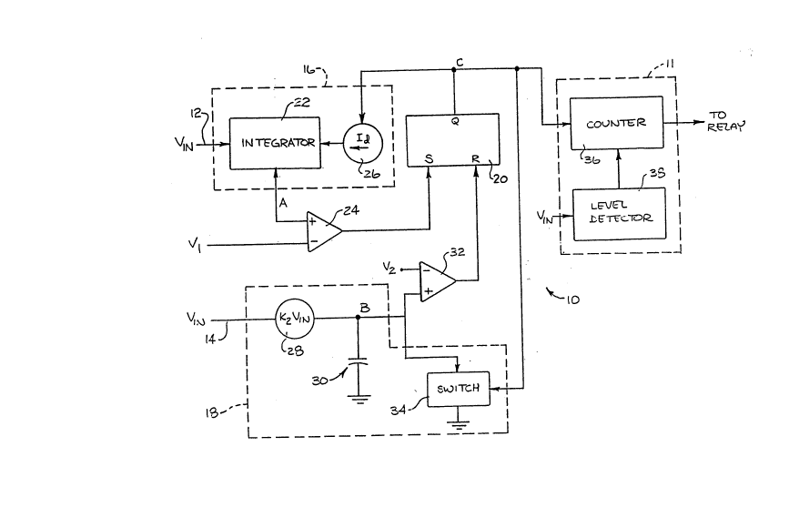
As illustrated in Fig.1, the voltage-to-frequency
converter 10 receives the input voltage Vin, and delivers the ;
frequency signal having a frequency fout which is -
proportional to the input voltage Vin. The input voltage Vin
appears on input lines 12,14 as a slowly fluctuating d.c.
voltage, which changes transiently in response to ;
fluctuations in the line current caused by increasing or
decreasing power demands. The input voltage Vin is
preferably received from a current transformer (not shown)
which produces a signal proportional to the current in the
conductor. The current signal is then converted to a voltage -~
signal through a rectifier. As the power on the power lines
increases above a predetermined level, the amount of time
that the power lines can handle the power decreases. Since
the output frequency fout is correlative to the current on
the line, the frequency fout is monitored to determine when
to trip the circuit breaker to interrupt the power line.
.
-
2 ~ A ~ 3 3
g
The voltage-to-frequency converter 10 uses two charging
circuits 16,18 to produce the output signal having a
frequency fout. The charging circuits 16,18 alternately
charge and discharge in a complementary fashion to control
respective portions Tl,T2 (see FIGS. 2 and 3) of the period T
of the output frequency fout. A set/reset flip flop 20
alternately switches each charging circuit 16,18 into the -
charge or discharge mode. The first charging circuit 16
includes an integrator 22, which receives the input voltage
Vin on its non-inverting terminal. The integrator 22
produces an upwardly sloping output at node A, as represented -
by the sloping portion Tl in Fig. 2A. The output of the
integrator 22 is connected to a first comparator 24 which
changes state when the output of the integrator 22 exceeds a
voltage setpoint V1. The output of the comparator 24 ~ -~
switches the "set" input of the set/reset flip flop 20. This -
causes the output of the flip flop 20 at node C to change
states, as shown by the transition between the portion T1 and
the portion T2 in Fig. 2C.
When the output of the flip flop 20 changes states, a
current source 26, which is connected between the integrator
22 and the flip-flop 20, begins to discharge the integrator
22. This discharge is depicted by the downwardly sloping -~
portions T2 of Fig. 2A. In addition, the transition of the
output of the flip flop 20 causes the second charging circuit
18 to begin charging, while the first charging circuit 16 ~
discharges, as shown by the portion T2 in Fig. 2B. This is ~-
accomplished by a current source 28 which receives the input
voltage Vin and which outputs a current having a magnitude
correlative to the magnitude of the input voltage Vin. The
output current charges a capacitor 30, which is connected to
the non-inverting input of a second comparator 32. A
reference voltage V2 is supplied to the inverting input of
the second comparator 32. When the voltage on the capacitor ;
30 exceeds the reference voltage V2, the output of the second
comparator 32 switches states to reset the output of the flip
flop 20. This transition of the flip flop 20 turns off the
,.
,.
current source 26 to allow the integrator 22 to recharge.
The transition also closes a switch 34, which is connected
between the capacitor 30 and circuit ground, to present a
discharge path to circuit ground, so that the capacitor 30
discharges quickly. This discharge is shown by the sharp
downward transition of the waveform in Fig. 2B.
The transitions of the output of the flip flop 20
produce an output frequency fout having a period T, which is
composed of the portions Tl and T2. The input voltage Vin
determines the charging rates for the two charging circuits
16,18, and thus the period T of the output of the flip flop
20. The charging time for each of the charging circuits
16,18 determines the time period of the respective portions
Tl,T2 of the output frequency fout, and the portions Tl,T2
are correlative to one another due to the common input
voltage Vin.
Fig. 3 illustrates waveforms similar to those of Fig. 2.
The input voltage Vin which produces the waveforms of Fig. 3
is greater than the input voltage Vin which produces the
waveforms of Fig. 2. A comparison between Fig. 2C and Fig.
3C shows that the greater input voltage Vin produces an
output having higher frequency. The greater input voltage
Vin charges the charging circuits 16,18 more rapidly, so that
the flip flop 20 switches at a higher rate. Since the output
of the first charging circuit 16 reaches the voltage setpoint
Vl in a shorter amount of time, the portion T1 of the period
T shortens. Likewise, the greater input voltage Vin causes
the voltage controlled current source 28 to output a higher ~;
current which charges the capacitor 30 to the voltage
setpoint V2 in a shorter amount of time, thus causing the
portion T2 of the period to shorten. The overall effect of
the faster charging times produces an output from the flip
flop 20 having a shorter period T and higher frequency fout.
Returning to Fig.1, the frequency signal from the flip -~
flop 20 is received by a tripping circuit 11. The tripping -`
::,"~
.
::
11 ,
circuit 11 may take a variety of forms, either analog or
digital, to process the output signal fout. A preferred
digital implementation of the tripping circuit 11 is shown in
Fig.l and includes a resetable counter 36 which receives the -
output frequency signal. The counter 36 counts the pulses
of the frequency signal and outputs a tripping signal to a
relay powering circuit (not shown) when the count exceeds a
tripping setpoint before the counter 36 resets. To reset the
counter 36, a level detector 38 receives the input voltage
Vin and controls the counter 36 responsive to the magnitude
of the input voltage Vin. The application of a reset signal
to the counter 36 causes the counter 36 to reset to a
predetermined count (typically zero).
The level detector 38 activates the counter 36 when the
input voltage Vin exceeds a predetermined setpoint, which
typically corresponds to about 110% of the current rating of ~-
the conductor. While activated, the counter 36 counts the
pulses from the output of the voltage-to-frequency converter ~ ;~
10, and asts as a delay device. If the input voltage Vin
drops below the predetermined setpoint by a predetermined
amount, which typically corresponds to about 105% of the
current rating of the conductor, the level detector 38
deactivates the counter 36. However, if the input voltage
continues to exceed the predetermined setpoint, the counter
36 eventually reaches a tripping setpoint, and outputs a
tripping signal which triggers the energization of a relay to
interrupt current flow in the conductor. The time that it ~;
takes the counter 36 to count to the tripping setpoint is the
delay time. Since a higher frequency causes the counter 36
to count at a higher rate, the counter 36 reaches the
tripping setpoint faster to provide a shorter delay time.
A schematic diagram for a preferred embodiment of the
voltage-to-frequency converter 10 is shown in Fig. 4. The
input voltage Vin is received on the non-inverting input of
an integrating operational amplifier 40 via a resistor 42. A
capacitor 44 is provided in the negative feedback loop of the
' ~
12
amplifier 40, and is charged at a rate dependent on the
magnitude of the input voltage Vin. The non-inverting input
of a comparator 45 receives the output of the integrating
operational amplifier 40. The inverting input of the
comparator 45 receives a threshold voltage Vl from a voltage
divider 48 formed by resistors 49 and 51. When the voltage
across the capacitor 44 exceeds the voltage Vl, the
comparator 45 outputs a "high" voltage (+5 to +15 volts) to
the "set" input of the set/reset flip flop 20.
The "high" voltage from the comparator 45 is received at
the base of a transistor 53 via a resistor 50, and causes the
transistor 53 to saturate and conduct current. Current
flowing through a resistor 52 from a positive voltage source
+V to the collector of the transistor 53 causes the voltage -
at the collector, which is the output of the flip flop 20, to
go to a "low" voltage (about 0.5 volts). The base of a
transistor 54 is connected to the collector of the transistor
53, so it receives the "low" voltage signal and becomes non-
conductive. When the transistor 54 is in a non-conductive
state, the base of the transistor 56 goes to a "low" voltage
because the emitter of the transistor 54 is connected thereto
via a resistor 55. Thus, the transistor 56 becomes non-
conductive also. The collector of the transistor 56 goes to
a "high" voltage since there is no voltage drop across a ~ -
resistor 58, which is connected between the collector of the
transistor 56 and the positive voltage source +V.
The output of the flip flop 20 triggers both of the
charging circuits 16 and 18. In the first charging circuit
16, the output alternately turns the current source 26 on and -~
off to discharge and charge the capacitor 44, respectively.
The voltage signal from the output of the flip flop 20 is
received on the base of a transistor 60 via a resistor 62.
When this signal is "low", it renders the transistor 60 non-
conductive. In the non-conductive state, there is no voltage
drop from the positive voltage source +V across a resistor
64, which is connected between the positive voltage source +V
13
and the collector of the transistor 60. Therefore, the
collector of the transistor 60 goes to a "high" voltage. The
base of a transistor 66 is connected to the collector of the
transistor 60, and receives this "high" voltage signal which
renders the transistor 66 conductive.
Two transistors 68,70 are connected in a current mirror
arrangement with the collector of the transistor 68 being
connected to the collector of the transistor 66. In this -
configuration, the conductive transistor 66 renders the
transistors 68,70 conductive also. A current Id flows to the
capacitor 44 through the collector of a transistor 72 which
has its emitter linked to the collector of transistor 70 and
its base linked to the collector of a transistor 73. The
base of transistor 73 is connected to the emitter of
transistor 66 while its emitter is connected to ground
through a resistor 78. The current Id is determined by the ~ -~
saturation characteristics of the transistors 66,68 and the
value of the resistor 78. The current Id is chosen to be
greater than the charging current Il flowing to the capacitor
44 from the amplifier 40. The charging current Il is present ~;
as long as the input voltage Yin is present, hence, the
discharging current Id must be greater than the charging
current in order to discharge the capacitor 44. Since the
charging current Id is substantially constant, the capacitor
44 discharges at a rate determined by the input voltage Vin
for a period T2 determined by the charging time of the second ~-
charging circuit 18.
While the first charging circuit 16 is discharging, the
second charging circuit 18 charges. The second charging ;
circuit 18 includes a charging element, shown here to be a
capacitor 82 which is connected between ground and the -~
collector of a transistor 80 which has its base connected to
the output signal of flip flop 20 and its emitter grounded. ~
The capacitor 82 is also connected to the voltage controlled -
current source 28, which comprises a non-inverting
operational amplifier 84 and resistors 86, 88, 90, and 92.
2 ~ J
The resistor 86 connects the inverting input of the
operational amplifier 84 to circuit ground, while the
resistors 90,92 are disposed in the feedback loop of the
operational amplifier 84. The operational amplifier 84
receives the input voltage Vin on its non-inverting input via
the resistor 88. The resistors 86, 88, 90, and 92 merely
serve to scale the output current I2 relative to the input
voltage Vin, and the resistance values of these resistors are
selected to partially adjust the magnitude of the output
current I2. When the output of the flip flop 20 is "low", it -
renders the transistor 80 nonconductive to prevent the
capacitor 82 from discharging to circuit ground through the
transistor 80. Since there is no path to ground, the current
source 28 charges the capacitor 82 with a current I2.
In Fig.4, the output of the capacitor 82 is connected to
the non-inverting input of an operational amplifier 95, which
is supplied with a reference voltage V2 on its inverting
terminal by a voltage divider 94 made up of resistors 96,97.
The output of the amplifier 95 is connected through a ~- ~
resistor 59 to the "reset" input of the flip flop 20 as ~-
defined by the junction of the base of transistor 56 and the
resistor 55 leading to the emitter of transistor 54. When ~-~
the voltage across the capacitor 82 exceeds the reference
voltage V2, the comparator 95 outputs a positive voltage to
the "reset" input of flip flop 20. The positive voltage
signal renders the transistor 56 conductive, thus causing its
collector to go to a "low" voltage. The collector of
transistor 56 is connected to the base of a transistor 57 `
which has its collector linked to the collector of transistor
54 and its emitter linked to the base of transistor 53
through a resistor 61. The "low" voltage signal at the
collector of transistor 56 thus renders the transistor 57 -~;
nonconductive. This in turn causes the base of transistor 53 ;
to go "low~ and renders the transistor 53 nonconductive. ~
This causes the collector of the transistor 53 to go "high" ~;
and closes the path to ground for the capacitor 82. The
"high" output of the transistor 53 also turns "off" the
"."~, .-.
--
current source 26 so that the current Il once again charges
the capacitor 44.
The following is a brief mathematical description
illustrating the relationship between the input voltage and
the output frequency for the voltage-to-frequency converter
lO of FIGS. 1 and 4. It should be noted that the change ~V
in the voltage at the output of the integrator 40 changes as
a function of the input voltage Vin (see FIGS. 2 and 3).
The period T1 is defined by the following equation:
Tl = (~V~rCl) .................. (1)
The period T2 is defined by the following equation:
T2 = (C2)rV2~ .................. (2)
I2
In equations (1) and (2), C1 is the capacitance of capacitor
44, C2 is the capacitance of capacitor 82, Vl and V2 are the
reference voltages mentioned earlier, and I1 and I2 are the
charging currents for the capacitors 44 and 82, respectively. ~
~V is defined by the following equation: - --
~V = (Id-IllT2 .................. .(3)
C1
where Id is the discharge current from the current source 26.
Using equation (3), and substituting values defined ~ ~
therein into equations (l) and (2), the period T is defined ~-
by the following equation: ;~
T = Tl+T2 = (Id~(C2~(V2~ - (Il)rC2) + rIl~ rC2~ ........ (4)
(I1)(I2) I2 I2
The values of the currents Il and I2 can be defined as ~;
Il=(Kl)(Vin) and I2=(K2)(Vin), where Kl and K2 are constants.
Thus, the total period T can be defined as: ;~--
T = rId~rV2)rC2) ................. .(5) --
(Kl)(K2)(Vin)2
, ,: .: .
16
Therefore, the output frequency fout can be defined as:
fout = 1/T = rKl)(K2)rVin~2 ............ (6)
(Id)(V2)(c2)
It will be apparent from equation (6) that the output : -
frequency fout is proportional to the square of the current
in the conductor since the input voltage Vin is correlative
to the current in the conductor.