Note: Descriptions are shown in the official language in which they were submitted.
2~12~3 25307-235
A TEol~~MODE DIELECTRIC RESONATOR CIRCUIT
BACKGROUND OF THE INVENTION
Field of the Invention
.
The present invention relates to a coupling circuit of
a transmission line to a TE0l~-mode dielectric resonator.
BRIEF DESCRIPTION OF THE DRAWINGS
Figure 1 schematically illustrates a prior art band-
pass filter employing a TE0l~-mode cylindrical resonator element,
where the side-walls of the waveguides are not shown in order to
simplify the drawing;
Figure 2 schematically illustrates a prior art band-
pass filter employing a TE0l~-mode half-cut cylinder resonator
element, where the side-walls of the waveguides are not shown in
order to simplify the drawing;
Figure 3 schematlcally illustrates a prior art band-
pass filter employing a TE0l~-mode half-cut cyllndrical
resonator element, connected with coaxial tranmission lines;
; Figure 4(a) is a sectional plan view schematically
illustrating a first preferred embodiment o~ the present
invention employed for connection with coaxlal transmisslon
lines;
Figure 4~b) 19 a vertlcal sectlonal vlew of the
embodIment of Flgure 4~a)s
~: Flgure 5 ls a vlew simllar to Figure 4(a) but
schematically illustratlng a second preferred embodlment;
Figure 6 is a vertical sectional vlew of a thlrd
preferred embodlment of the present lnvention;
-- 1 --
. .
.: :, :
.
. .
:" ~
. .
. ~
',
25307-235
2012003
Figure 7 shows an inner side plan view of a ceramic
substrate employed in Figure 6 embodiment;
Figure 8 shows a perspective view of the components
employed in the Figure 6 embodiment;
Figure 9 shows an outer side plan view of the ceramic
substrate employed in Figure 6 embodiment;
Figure 10 shows a perspective view of the complete
Figure 6 filter;
Figure 11 shows bandpass characteristics of Figure 6
filter;
Figure 12 shows an enlargement of Figure 11 bandpass
characteristics in the vicinity of the resonant frequency;
Figures 13(a) and 13(b) show a fourth preferred
embodiment of the present invention;
Figure 13(c) shows the opposite side of the ceramic
substrate shown in Figure 13(b);
Figure 14 shows a fifth preferred embodiment of the
present invention; and
Flgure 15 shows a sixth preferred embodiment of the
present invention.
Description of the Related Art
A prior art TE0l~-mode dielectric resonator employed
~;~ in a bandpass filter and the method of coupling with its
external circuit are qhown ln Figure 1 through Figure 3. In
`:
Figure 1, between two standard waveguldes (l.e. TElo mode wave-
`~ guides) 1 and 1' there is connected a second waveguide 2 which is
in a cut-off state for the electromagnetic wave to be now
- la -
~. ~ - . ...
,.. ~ .. . . . - . .:
- . . .
. -
. . ~ . . :- :
25307-235
20~2~03
transmitted through the standard waveguides 1 and 1'. A TEolC-
mode cylindrical dielectric resonator element 3 is installed in
the second waveguide 2 via a metal stage 4 mounted on its side
wall parallel to the larger side walls of the standard wave-
guides 1 and 1'. The resonator element 3 is coupled magnetically,
i.e. via magnetic flux, with both the standard waveguides 1 and
1', so as to allow only the resonator element's resonant
frequency to transmit through the cut-off waveguide 2. In this
circuit configuration, the stage 4 causes an increase in space
occupancy of the circuit.
In order to reduce the space occupancy, a
- lb -
''"'' ' ~ '~ :
,: ~
.: :
;. ~: . -.-:
'
~ . .
, 25307-235
29120~3
configuration shown in FIG. 2 has been proposed, such as
disclosed in Japanese TokuKai Hei-1-14~701. In this
circuit configuration, a half-cut cylindrical dielectric
resonator element 5 has its flat surface adhered to a
shorter side wall of the cut-off waveguide 2, and is
magnetically coupled with the standard waveguides 1 and 1'.
In FIG. 3, a half-cut dielectric resonator element 5
is adhered on an inner wall of a metal case 7 so as to
interconnect coaxial lines 6 and 6'. In this circuit
configuration, an extension of each of the lnner conductors
of the coaxial lines 6 and 6' i8 terminated on the metal
case 7 and forms a loop 6a which is magnetically coupled
with the half-cut cylindrical resonator element 5.
However, there are problems in that in the FIG. 2
~5 configuration the overall circuit size i8 little reduced
even though the resonator element is reduced into a half
size~ and in the FIG. 3 configuration the loops 6a require
the space in the case 7. The same problem is in a circuit
configuration employlng a quarter cut TE0lO-mode dielectrlc
resonator element reported in "IEEE Tr~hsactlon on
Microwave Theory and Techniques", vol. MTT-35, No. 12, Dec.
1987, p.ll50-1155. Thus, there is notmuch llkelihood of
further size reduction ln the above-descrlbed circuit
configuration. Therefore, a new coupling clrcuit which can
en~oy the advantage of the compact half or quarter cut
cylindrical dielectric resonator has been expected.
,' , .
: .
~ ' .
2012003
25307-235
SUMMARY OF THE INVENTION
It is a broad object of the invention to provide an
improved dielectric resonator.
It is another object of the invention to provlde a
compact circult confi~uration for coupling a half or quarter-cut
cylindrical TEOl~-mode dielectric resonator to an outer
transmis~ion llne.
It is another object of the invention to provide a
circuit configuration suitable for mounting a half or quarter-eut
cyllndrical T~Ol~-mode dlelectrlc resonator onto a printed cirauit
board.
A resonator element formed of a half or a quarter of
dieleetrle eyllnder eontaets an eleetrieally conductlve plane vla
the resonator element's radlally cut slde which includes the axis
of the cylinder, aceordingly, resonates ln TEOl~-mode. On an
opposite slde of the electrically conductive plane there i~
provlded an unbalaneed transmission line, for example, of a strip
line type or a eoaxial line type. An end of the transmlssion llne
18 eleetromagnetieally eoupled, vla a dleleetrle material ln the
tran~mlssion llne or dlreetly, wlth the radlally eut slde of the
resonator element through an openlng provlded on the eleetrleally
eonduetlve plane.
In ~ummary, the pre~ent lnventlon provides a dieleatrle
resonator eomprlslng. a resonator element formed of a dleleetrle
ayllnder portion, the dleleetrle eyllnder portlon havlng an axis,
a radlal slde lylng ln a plane eontalnlng the axls of the
dleleetrle eyllnder portion and two sides orthogonal to the axl~
``~q A
~, . . . . .
.:: : . `
20120~3
2s307-235
an electrically conductive plane having a first surface in contact
with the radial side of said resonator element, said electrlcally
conductlve plane havlng at lea~t one opening, the radial side of
said resonator element facing the at least one opening; and a
transmission line located opposite from said resonator element
with respect to said electrically conductive plane, said
transmission line operatively connected to the at least one
opening, coupling an electromagnetic wave carried on said
transmission line vla the at least one opening to said resonator
element.
The above-mentioned features and advantage~ of the
present invention, together with other ob~ects and advantages,
which will become apparent, will be more fully descrlbed
herelnafter, wlth reference being made to the accompanylng
drawlngs which form a part hereof, whereln like numerals refer to
llke part~ throughout.
DBSCRIPTION OF THE PREFERRBD ~MBODIMENTS
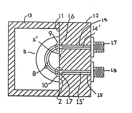
With reference to Flgures 4(a~ and 4~b), a dlelectric
resonator element 5 1B formed of a dlelectrlc material, such as
~ZrSn~T104 whose dielectrlc constant 18 as high as 36.5 or
Ba2TigO20 whose dlelectrlc constant i8 39.8. The dlelectrlc
resonator 5 18 in the shape of a half-aut cylinder havlng a flat
slde 5' whlch lncludes the axls (not shown ln the flgure) of a
dlelectrlc cyllnder of, for example, 6 mm dlameter. The flat slde
5' 1~ referred to herelnafter as a radlally cut side. The half-
¢ut cyllnder ls also cut with two planes orthogonal to the axl~ of
the ayllnder so as to leave, for example, 2.3 mm
:
. `' '~ :
,~ .
25307-235
2~12Q~3
thickness. The radially cut side 5' is adhered to a metal wall
11 of a resonator base 12 typically with a generally available
epoxy resin. The metal wall 11, being electrically conductive,
acts as a mirror to form an image of the half-cut cylinder
dielectric resonator element 5, so that the half-cut cylindrical
dielectric resonator element 5 resonates in a TE0l~-mode like a
fully cylindrical dielectric resonator element. The resonant
frequency of the resonat~r element varies depending on the
element's dimensions and its dielectric constant. First and
second coaxial transmission lines 14 and 15, each having
typically 50 ohm characteristic impedance, are provided
normally to the metal wall 11 through the resonator base 12.
Each of coaxlal transmission lines 14 and 15 is typically
composed of 2.1 mm outer diameter, 0.63 mm inner conductor
diameter, and Teflon ~CF4) filled therebetween. End 16 and 17
of each inner conductor 14' and 15' of respective coaxial
transmission lines 14 and 15 faces the radially cut side 5' at
a predetermined dlstance d (denoted in Figure 4~b)), for
example, 0.5 mm. An electromagnetic wave signal transmltted on
the lnner conductor 14' of the first coaxlal transmisslon line
14 ls electromagnetically coupled to the radlally cut slde 5'
of the resonator element 5 vla capacltance formed at the above-
descrlbed distance. That ls, current flowlng from the inner
conductor 14' through the capacitance excites the resonator
element 5, and further flows along the TE0l~mode electric field
8 ln the resonator element 5 shown in Figure 4~a). The term
"coupling" is referred to so as to express this phenomena. This
~`
_ 5 _
..~...~ .
~'.~' .. .', ,
.
' : ,
.
2~2003 25307-235
current reaches the inner conductor 15' of the second coaxial
line 15, in the same but reverse way as the first coaxial line
14, only when the frequency of the signal causes TE10~-mode
resonance in the resonator element 5. Any frequency other than
the resonant frequency does not reach the second coaxial line
15 and reflects back to the first coaxial line 14. Thus, the
resonator element 5 acts as a bandpass filter. The other ends
of the coaxial lines 14 and 15 are connected to coaxial connectors
17 and 18, respectively. Thus, the circuit of Figure 4 can be
handled as an independent filter, easily detachable from coaxial
cables. xetal cap 13 is electrlcally connected, ior example
-- 6 --
,~
:
.~, .,,, ~..................... . .
' - :
:' . . :
'; ' ': ~, ,
2 0 ~ 2 ~ ~ 3 25307-235
soldered, to the resonator base 12 so that the resonator element
5 is confined in its cavity as well as shielded from other
circuits.
Electric field strength expressed with density of
2 ~
electric fields 8 is weak at the peripheral portion or at
the centre portion of the half-cut cylinder 5. A coaxial
transmission line connected to the higher electric field
portion provides a closer coupling, as well as less
coupling at a weaker electric field portion. Therefore,
j the coupling between the transmission line and the
resonator element S can be varied by choosing the location
of the transmission lines 14 and 15 along the radial
direction of the dielectric cylinder. The coupling between
the transmission line and the resonator element S can be
adjusted also by the capacitance value at the distance
between the inner conductor ends 16 or 17 and the radially
cut side 5' of the resonator element 5. The closer
coupling between the transmission line and the resonator
element 5 provides the wider pass-band width of the filter.
In order to achieve impedance matching of the input
transmission line 14, locations of the two transmission
lines 14 and 15 are preferably chosen at the symmetric
positions with respect to the axis of the resonator element
, 20 5.
FIG. 5 shows a second preferred embodiment of the
present invention, as a modification of FIG. 4 first
preferred embodiment. Each of inner conductors 14' and 15'
and their ends 16' and 17', of the coaxial lines, are
printed on a ceramic substrate ~not shown in the figure).
The ends 16' and 17' are made wider than the 50 ohm
-- 8 --
. ~
., . .,.~
''. ,
,
2 ~ 3
transmission line portion 14 and 15 so as to form a
properly increased capacitance with the radially cut side
5' of the resonator element 5. In order to adjust the
capacitance, the shape of the ends 16' and 17' can be
adjusted by removing the printed conductor by means of, for
example, sand blasting. Advantage of FIG. 5 configuration
is in that the coupling capacitance value can be precisely
controlled.
A third preferred embodiment of the present invention,
where the input and output transmission line circuits are
formed of strip line type transmission lines, is
schematically illustrated in FIG. 6 showing a vertically
cut cross-sectional view; FIG. 7 showing an inner surface
plan view of its ceramic substrate; FIG. 8 showing a
lS perspective view of the composing elements; FIG. 9 showing
an outer surface plan view of the ceramic substrate; and
FIG. 10 showing a perspective view of the complete filter
mounted on a mother board. According to a widely employed
method, electrically conductive planes 22a of, for example,
: 20 copper, i9 formed upon a surface of, for example, a 0.65 mm
thick alumina ceramic substrate 22, and is provided with
two openings 22h of typically 0.8 mm diameter and spanned
by 2 mm, by chemical etching or sandblasting so as to
expose part of the ceramic substrate 22, while circular
2S patterns 22b and 22c, as coupling electrodes, are left at
; the centre of each opening. In the same way, on the other
_ g _
.: .
~ . . . .
~ , .,
: . .
: .
.
- , : ~
~ . ~ . .-,
2~:~2~3
surface of ceramic substrate 22, there are formed an input
strip electrode 22f, an output strip electrode 22g, each
having 0.6 mm width, and a ground plane 22a'. Shorter
sides of substrate 22 may be also coated with an
electrically conductive material so that both the ground
planes 22a and 22a' are electrically connected. Each of
strip electrodes 22f and 22g, together with this side of
ground plane 22a and the 0.65 mm thick ceramic substrate
therebetween, constitute strip-line type 50 ohm
transmission line. Hatched portions in FIGs. 4 and 5
indicate the exposed ceramic substrate 22. At the centers
of coupling electrodes 22b and 22c, there are provided
through-holes 22d and 22e coated with electrically
conductive material so as to electrically connect each of
the coupling electrode 22b and 22c to ends of the strip
electrodes 22f and 22g, respectively. Each of the opposite
ends 22f' and 22g' of strip electrodes 22f and 22g
vertically extends along thin side of the ceramic substrate
22 so as to be terminals to be connected with external
circuit by soldering. Resonator element 21a is
substantially the same as the resonator element 5 used in
the first preferred embodiment. The radially cut side
21a-1 of the resonator element 21a is adhered onto the
metal plane 22a as well as the openings 22h, in the same
way as those of FIGs. 4 and 5. A metal cap 23 is soldered
onto the metal plane 22a in order to shield the resonator
-- 10 --
2~12~3
element 21a from the other circuits, as denoted with the
numeral 24. Thus completed filter unit 21 is mounted onto
a mother circuit board 28 by soldering the ground planes
22a and 22a' onto a ground plane 29, as well as terminals
22g' and 22f' to a strip electrode 26, each of a mother
circuit board 28. Degree of the coupling between the
transmission line and the resonator element is determined
by the size of openings 22h, the size of the coupling
electrodes 22b and 22c and the location of the openings
measured from the axis of the half cylinder. The coupling
electrodes 22b and 22c provide relatively large capacitance
value, resulting in a close coupling with the resonator
element 21a.
In order to achieve relatively loose coupling with the
resonator element 21a, the coupling electrodes 22b and 22c
and the through-holes 22d and 22e may be omitted. This
case is not shown in the figure. In this case, the degree
of the coupling is determined by the capacitance between
the strip electrode and the resonator element, that is, by
the size of the opening, the area of the strip electrode
facing the resonator electrode through the opening, and the
thickness as well as dielectric constant of the ceramic
substrate 22 existing therebetween.
Bandpass characteristics of FIG. 6 filter are shown in
FIGs. 11 and 12. FIG. 11 shows frequency characteristics
from 1 to 26 GHz, where a peak at 9.848 GHz is of the TE
~,~., .
..... ~ , , ~ ~
:: . . . .
. .
.
:: .
.
, ,
; -. . .
,: .
2~2~3
mode resonance of the resonator element, while other peaks
existing at higher frequency band than the TEolO mode
resonance are of higher mode resonances of the resonator
element and of the resonance of the cavity formed with cap
23. FIG. 12 shows an enlargement of the FIG. 11 bandpass
characteristics in the vicinity of the TEolO mode
resonance. The - 3 db band width is 12.8 GHz for the
centre frequency 9848.425 MHz, and the insertion loss is
16.5 db. The insertion loss will be much reduced by
employing more suitable material for adhering the resonator
element to the substrate.
Size of bandpass filter unit 21 shown in FIG. 6, used
for 10 GHZ band, achieved 7 mm high x 8 x 14 mm cap and 12
x 18 mm substrate. Thus, the filter volume is as small as
approximately 1.4 cc, wh$ch is a half of 2.8 cc of case 7
in FIG. 3 of the prior art filter employing coupling loops.
Moreover, FIG. 6 structure is suitable for being easily
handled and mounted on a strip line type mother circuit
board, which is the most commonly employed today, as well
as allows the mother board to be compactly finished.
~ variation of the substrate embodied in the third
preferred embodiment i8 shown in FIGs. 13~a) and 13~b).
FIG. 13~b) explains assembling of the components. FIG.
13~c) shows the opposite surface of ceramic substrate 32
shown in FIG. 13~b). Cap 23 and resonator element 21a are
substantially the same as those of FIG. 6. Ground planes
29~2~03
32a and 32a' coated on the both surfaces of ceramic
substrate 32 are electrically connected with each other via
a plurality of through-holes 37 provided through the
ceramic substrate 32 or via metal coat on the short sides
of the ceramic substrate 32, and are soldered to a metal
substrate 31. Metal substrate 31 is provided with two
channels 43, which are, for example, 3 mm wide, 0.7 mm
deep, and extend so as to face the strip electrodes 34.
Between the two channels there is left a 1 mm wide bank 36.
When ceramic substrate 32 is fixed onto metal substrate 31,
the strip electrodes 34 are electromagnetically shielded in
channels 33, respectively. Bank 36 act as an
electromagnetic shield between input and output
transmission lines 34. Strip electrodes 34 do not need
extended portion 22f' and 22g' along the short sides of the
ceramic substrate 22 as in FIG. 8. However, each end of
strip electrodes 34 is extended with ribbon electrode 35
soldered thereto. Metal substrate 31 having the filter
unit 30 thereon is fixed to a mother board (not shown in
the figure) with screws 38 penetrating the openings
provided on the metal substrate 31, then the ribbon
electrodes 35 being flexible are easily soldered to a
circuit on the mother board. This configuration allows an
easy handling as well as quick mounting of the filter unit
onto the mother board.
A fourth preferred embodiment of the present invention
- 13 -
, :
: . . .
- ~
25307-235
2~ 20~3
is shown in Figures 14 (a) and (b), where a plurality of the
resonator elements 43A through 43C are employed in a single case
412. Figure 14(a) shows a perspective view of the filter unit,
whose top lid 412' is disassembled. Figure 14 (b) shows a cross-
sectional plan view of Figure 14 (a) filter. Each of the
resonator elements 43A through 43Cis essentially the same as
that of Figure 4 first preferred embodiment. Radially cut sides
42A, 42B and 42C of respective resonator elements 43A through
43C are adhered in line onto a metal wall 41 of case 412. A
coaxial input terminal 417 according to the structure of Figure
4 first preferred embodiment or Figure 5 second preferred
embodiment is arranged so as to couple the first resonator
element 43A, at a farther side than the axis of the half
cylinder of the resonator element 43A from the next resonator
element 43B. The resonator element 43B located between the first
and the last resonator elements is provided with no external
coupling means through the wall 41. Each of the resonator
elements 43A through 43Cis mutually coupled with the adjacent
resonator element by magnetic flux 49A and 49B of the TEOl~s-mode
as shown with dotted lines. Signal input from the input terminal
417 exciting the first resonator element 43A thus propagates
along on each resonator element to the last resonator element
43C.A coaxial output terminal 418 similar to the lnput terminal
417i9 provided so as to couple the last resonator element 43C,
at the farther side from the previous resonator element 43B with
respect to the axis of the half cylinder of the resonator
element 4 3C. Thus, only the resonant frequency of the resonator
-14-
. ` '
~, ' '
25307-235
2~12003
elements 43A through 43C can be output from the output terminal
418. Degree of the mutual coupling between the neighbouring
resonator elements determined by their distance determines the
filter's pass-band width. A metal lid 41~' covers the top
opening of the case 412. Metal screws 419A through 419C are
provided in screw holes on metal lid 412', and extends there-
from to over respective resonator elements. Resonant frequency
of each resonator element can be finely adjusted by rotating
the corresponding screw. The Figures 14 configuration is
advantageous in that the space occupied by the coupling loops
from/to the input/output circuit can be saved. It is apparent
that Figure 6 strip-line type input/output circuit can be also
embodied in Figure 13 multiple resonator element configuration,
though no figure is given therefor.
Though in Figures 14(a) and (b) the input and output
terminals 417 and 418 are located respectively farther sides
than each element axis, it is apparent that the input and/or
output terminal~s) ma~v be located nearer side than respective
element axis as denoted wlth arrows 417' and 418'.
Figure 15 shows a fllter unlt as a fifth pre~erred
embodiment of the present invention. This configuration is
:
. :
.
2~2003
suitable for a use in relati-vely low frequency band, such
as below several hundreds Mega-Hertz band. Therefore,
sizes of resonator element 50, ceramic substrate 51 and cap
52 are larger than those of FIG. 4 or FIG. 6 configuration;
S however the structures are quite similar thereto, except
that the outer surface Sl' of substrate 51 has no coaxial
lines nor strip electrodes. Electrically conductive
through-holes 53 are provided through the ceramic substrate
51 so as to face the centers of the openings of the metal
plane ~not shown in the figure) on the inner surface 51''
of the substrate. Diameter of the through-holes, locations
of the through-holes, and the distance between the ends of
the through-holes and the radially cut side of the
resonator, determine the degree of the coupling.
Therefore, coupling electrodes may be additionally provided
at the ends of the through holes as the FIG. 7
configuration. Electrically conductive leads 54 are
soldered to the through-holes 53, as input and output
terminals of the filter unit from and to other circuit.
When a 1008e coupling is required, the above-described
electrically conductive through-boles may be omitted, and a
coupling electrode ~not shown in the figures) may be
provided on the outer surface 51' of the ceramic substrate
51 in place of the through-holes. Then, leads 54 are
soldered to the coupling electrodes on the outer surface
51'. Outer ground plane (not shown in the figure) coated
- 16 -
. ~, .
.. ~ . . .
.
.
.
.
~2~3
on the outer surface 51' of the substrate 51 is connected
to inner ground plane via the electrically conductive
through-holes ~not shown in the figure) provided through
ceramic substrate 51 or via metal coating tnot shown in the
figure) on the short side of the ceramic substrate 51. A
grounding lead 55 is soldered to the outer ground plane at
the centre of input/output leads 54. The grounding lead 55
located between input and output leads 54 is effective to
electromagnetically shield the two leads 54. The grounding
through-holes may be omitted, when the inner ground plane
is grounded by other means. Grounding lead 55 may be
omitted, when the ground plane 51 " can be grounded by
other means. In addition to the advantage of the filter's
less space occupancy, less number of the components is
advantageous for cost reduction of the filter.
Though a half-cut cylinder type resonator element is
referred to in the above preferred embodiments, it is
apparent that the concept of the present invention can be
embodied for coupling the input/output circuit to a
quarter-cut cylinder resonator element. The quarter-cut
cylinder resonator element is such that two of the radially
cut sides, each including the axis of the cylinder and
orthogonal to each other, cut a dielectric cylinder so as
to leave a quarter of the cylinder. The radially cut sides
are contacted respectively with two metal walls orthogonal
with~each other. Each metal wall acts as mirror to form an
.. . .
.:
. .. .
20~ 2~03
image of the quarter cylinder so that the quarter-cut
cylinder resonates equivalently in the TEo1or mode of a
complete cylinder. Quarter-cut cylinder resonator elements
are reported in tbe above-cited IEEE Transaction. When a
quarter-cut cylinder resonator element is provided with
both the input and output terminals, the terminal is
provided on each of the two orthogonally arranged metal
walls.
Though in the above-described preferred embodiments a
radially cut side of the resonator element is contacted
with a metal wall, it is apparent that radially cut side of
the resonator element may be metalized with an electrically
conductive material, excepting the openings for the
electrostatic coupling. The metalization is carried out by
lS a generally employed technique, such as plating,
sputtering, sintering or printing of copper, gold or
silver, etc. The metalized side of the resonator element
may be further contacted wi~h the metal wall referred to in
the above embodiments, or may be directly employed for
constituting the transmission line. The metalization of
the resonator element reduces improves the insertion 1088
in the bandpass characteristics caused from the used of
organic adhesive material.
The many features and advantages oP the invention are
apparent from the detailed specification and thus, it is
intended by the appended claims to cover all such features
- 18 -
.: .
' '; , : . .
2~ 2~03
and advantages of the system which fall within the true
spirit and scope of the invention. Further, since numerous
modifications and changes may readily occur to those
skilled in the art, it is not desired to limit the
S invention to the exact construction and operation shown and
described, and accordingly, all suitable modifications and
equivalents may be resorted to, falling within the scope of
the invention.
,
K
- 19-
~, :, ~:
,