Note: Descriptions are shown in the official language in which they were submitted.
- 1- 2~ 2~ `
ELECTROCHROMIC DEVICES COMPRISING METAL SALTS
IN AN ION ~ONDUCTIVE MATERIAL
Field of the Inven~ion
S
The present invention relates to electrochromic
devices which exhibit coloratîon and bleaching thereof
due to an induced electric field. More particularly,
this invention relates to electrochromic devices which
include a layer comprising metal salts dispersed or
dissolved in an ion conductive material. Herein this
layer is termed an "electrochromic matrix material lay~r".
Back~round of the Invention
In an electrochromic device, a physical/chemical
change is produced in response to an induced electric
field. The result is a chan~e in the reflective (or
transmissive) properties of the device with respect to
electromagnetic radiations, e.g., W , visible and IR
radiations. Such devices, one embodiment being shown as
item 10 in Figure 1, generally comprise a film of
electrochromic material 12 and an ion-conductive
insulating layer 14 which functions as an electrolyte
layer. The film and the electrolyte layer are in surface
contact with each other for exchange of ions between the
electrochromic film and the ele~trolyte layer. Two
conductive electrode layers, 16 and 18 in Figure 1, at
least one of them being transparent, are disposed on the
opposite outer surfaces of the film and the electrolyte
layer to provide means for applying a voltage across the
combined thickness of the electrochromic film and the
electrolyte layer. As shown in Figure 1, electrode
layers are provided on substrates 20 and 22, which
substrates may be of a material such as glass. Depending
,
.~ .
20~;~23~
on the ion providing and ion storage capaci~y of ion
conductive layer 16, a counter electrodè located between
ion conductive layer 14 and electrode layer 18 may be
used. The electrodes are provided with external
electrical leads 24 and 26 connected to a voltage
providing source 28. Application of a voltage of proper
polarity across the electrodes causes coloration of the
electrochromic layer. By reversing the polarity of the
applied voltage, the colored electrochromic layer will be
uncolored (bleached). Changing from the bleached state
to the colored state or from the colored state to the
bleached state is termed "switching". The electrochromic
material may be "persistent" in its colored state which
means that it has the ability to remain, after removal of
the electric field, in the absorptive state to which it
is changed, as distinguished from a substantially
instantaneous reversion to the initial state. The length
of time a material is persistent is called its "open
circuit memory" or simply "memory". Electrochromic
devices of this type have been described for several
uses, such as for image display, for light filtering,
etc. See, e.g., U.S. Patent Nos~ 3,708,220, 4~194,812;
4,278,329; 4,645,308; 4,436,769; 4,500,878; 4,150,879;
4,652,090; 4,505,021; and 4,664,934.
~ In such devices, the electrochromic film usually `
; comprises an inorganic metal oxide material, most
commonly a transition metal oxide, in particular:
tungsten oxide. When tungsten oxide is the
electrochromic material, the electrolyte layer is adapted
to provide a positively charged light cation, preferably,
a proton or a lithium ion. The electrolyte layer may be
a liquid electrolyte solution like lithium perchlorate in
propylene carbonate or a gel electrolyte like polyvinyl
butyral-methanol do~ed with LiCl. The electrolyte layer
, . .
., - . ~ , . .
~',:. :. - '-, "': . '`' ' ' , . - ' ' ;~
~0122~ 5
may also be a solid electrolyte which comprises polymers
or copolymers containing acidic groups such as
polystyrene sulfonic acid, propylene oxide or
polyethylene oxide.
It would be desirable, however, to have an
electrochromic device which comprises less layers and is
hence less complex to fabricate. Additionally, it would
be desirable if the device, in addition to being able to
reduce transmission of visible light, would also be able
to substantially reduce transmission of IR wavelength
radiation, i.e., keep radiation of the type which
generates heat from passing through the device. This
would be particularly useful if the device is used as a
window of a building or automobile.
Brief DescriPtion of the Invention
. :- .
The present invention is directed to an
electrochromic device comprising a substrate: a first
electrode member provided on the substrate; an ~ -
electrochromic matrix material layer in contact with the
first electrode member; and a second electrode member in ~;~
contact with the electrochromic matrix material layer, at ;-
least one of the first and second electrode members being
transparent, the electrochromic matrix material layer
consisting essentially of a substantially uniform mixture
of: (i) a metal salt component selected from the group
consisting essentially of halides, acetates, nitrates,
30 sulfates, and phosphates of metals selected from the ;~
group consisting essentially of copper, cobalt, nickel,
lead, molybdenum, rubidium and tin; (ii~ an ion
conductive material component selected from a group ~
consisting essentially of solid electrolytes and gel -
electrolytes; and an ion conduction enhancer component
: '
.
2~ 2~5
selected from the group consisting essentially of lithium
salts and sodium salts. Preferably, the metal salt is
present in the matrix layer in an amount sufficient to
provide a maximum thickness of between about 500 to lOOOA
of the metal on an electrode member when a voltage is
applied across the electrodes. The device may further
comprise a second substrate adjacent to the secand
electrode member. According to another aspect of the
invention, it is directed to the method of making the
above device.
When a voltage is applied across the electrodes
of the device, the electrode member which functions as
the cathode takes on a metallic appearance which makes
the device useful as a display device. Additionally,
embodiments of this device are particularly useful as
windows of buildin~s or automobiles since ~hey are
capable of more effectively reflecting IR radiation than
are conventional electrochromic devices. Thus
embodiments of the present invention device, if used as
windows, offer an enhanced ability over prior art
electrochromic devices to keep heat out of the building
or automobile, while at the same time being capable of
keeping heat within the building or automobile from
escaping through the device. This is in addition to the
ability of these devices to control the amount of visible
light which may enter the building or vehicle. Still
further, it has been found that embodiments of the device
of the present invention are able to be switched to the
colored state by means of a relatively low voltage
applied across the electrodes.
The thickness of the metallic layer formed
during operation of the device and hence the
corresponding reduction in transmission of radiation by
`:
.
.. : . . . . . . .
~: , . , ~ . . . .
:, :~ . ,
'. ! ` - ~ , , : ~ `
:.,: ` . `' ` :'~ ` '
:': '., ' ': ' , .
20~2~5
the device can be controlled by the length of time a
voltage is applied across the electrodes of the device.
That is, the longer the voltage is applied, the thicker
the metallic layer formed with a corresponding increased
reduction in transmission of radiation through the
device. Thus the device advantageously has a variable
and controllable transmittance. According to aspects of
the invention comprising a linear cathodic electrode
which is discussed in detail hereinafter, it is also
advantageously possible to provide a device having a
metallic layer of graded thickness so as to provide
different portions of the device with varying
transmission levels.
Brief Descri~tion of the Drawin~s
Figure 1 is a schematic representation of an
electrochromic device, in cross-section, according to the
prior art.
Figure 2 is a schematic representations of an r
embodiment of an electrochromic device, in cross-section,
according to this invention, before and after a voltage
is applied across the electrodes of the devicet
Figure 3 is a schematic representation of an
j embodiment of an electrochromic device, in cross-section,
according to another aspect of this invention.
Detailed Descri~tion of the Invention -
~.'` .
As disclosed above, the electrochromic device of
this invention comprises a substrate; a first electrode
member; an electrochromic matrix material layer; and a
second electrode member. The electrochromic matrix
~.
,
, . .
'-.'~"~ ~ :. :,
- 6 - ~0~2~S
material layer (prior to application of a voltaqe across
the electrode members) consists essentially of a
substantially uniform mixture of (i) a metal salt
component, (ii) an ion conductive enhancer component and
(iii) an ion conductive material component. The device
may further comprise a second substrate adjacent to the
second electrode member.
One aspect of the invention will be further
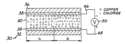
understood by reference to Figure 2. This figure depicts
a cross-sectional view of an embodiment of a device 30
according to the invention taken along a line
perpendicular to a surface of a substrate of the device,
before and after application of a voltage across the
electrodes of the device~ The device 30 in Figure 2
comprises glass substrate 32 in contact with transparent
electrode member 34 and glass substrate 36 in contact
with transparent electrode member 38. The device further
comprises a layer of electrochromic matrix material 40
according to the present invention, shown before, "a",
and after, "b", application of a voltage across the
electrodes. The electrochromic matrix layer 40 (before
application of a voltage across the electrodes) consists
essentially of a substantially uniform mixture of
components ~i), (ii), and (iii) as described above. In
the particular embodiment shown in Figure 2, these
components are copper chloride, lithium nitrate and
polyvinyl butyral gel, respectively. Section "a" o~ the
matrix material layer 40 of the Figure 2 device 30 shows
the copper chloride (metal salt component) substantially
uniformly dispersed throughout the matrix layer.
Although not shown, the ion conduction enhancer also
would be substantially uniformly dispersed throughout the
matrix material layer 40, section "a". This particular
embodiment of the matrix material layer would appear
.
: .
.: .
2()~2~5
light yellow in color as initially provided in the
device, i.e., prior to application of a voltage across
the electrodes. The intensity o~ the color o~ the
initial transparent, yellow matrix layer would depend
only on the concentration of the copper chloride in the
matrix material since the ion conduction enhancer present
in the matri~ material is colorless. Increasing the
amount of ion conduction enhancer, however, serves to
increase the conductivity of the ion conductive material
component ~i.e., the electrolyte) which, in turn,
increases the rate at which a metal layer is formed at an
electrode member when a voltage is applied.
During operation of the device, a voltage is
applied across the electrodes by means of leads 46 and 48
connected to a d.c. voltage source 50 as shown in
Figure 2. When a voltage is applied across the
electrodes, it is believed that the metal ions (cations)
of the metal salt present in the matrix material layer 40
migrate toward the electrode member of negative
polarity 38 (i.e., cathode or "working electrode") as
shown in Figure 2, section "a". The metal ions would be
converted to metal atoms at the cathode 38 to provide a
metal layer thereon and provide a metallic reflective
layer to the device which would inhibit transmission of
impinging radiation through the device. In the
particular matrix layer described above, the matrix layer
(and thus the device) would change from a light yellow
transparent layer having a transmittance of perhaps about
60% (depending on the metal salt concentration) to an
opaque (i.e., having about 0% transmittance) layer
; comprising a metallic copper layer. The transparency (or
opaqueness) of the device after a voltage has been
applied would depend on the thickness of the metal layer
~ 35 (in thls instance, copper) which plates out on the
:'
,,
,, ~ . .: , ~ . , . . -. . .
, :. - , . .
: , .. . . ~ ,
- ~ , . .. : : : ,- : . -
... . . . . . . .
.:
~Ql~Z~5
cathode. A thicker metal layer would provide a less
transparent device. The anions of the metal salt (e.g.,
the chloride ions of the particular embodiment discussed
above) would be expected to migrate toward the positive
electrode member (i.e., anode) if the ion conductive
material allows for the ionic transport of the anion, as
shown in Figure 2, section "b". In this particular
embodiment of the device, some of the chloride ions may
be oxidized to chlorine gas at the anode. The use of a
counter electrode between the matrix material layer and
the anode of the device is useful to minimize formation
of gas at the anode. U.S. Patent 4,768,865 discloses
that formation of gas at an anode of an electrochromic
device may be minimized by use of a grid shaped anode.
If the ion conductive material allows for the
ionic transport of the cation and anion of the ion
conduction enhancer, they would also be expected to move
toward the cathode and anode, respectively.
~ enerally, it has been found that the device of
this invention has a short term memory, i.e., it readily
., . , ~
reverts to its initial (uncolored) state when the applied
; electric field is removed. For e~ample, in the
particular embodiment device described above, when the
electric field is removed the metallic copper layer -
; disappears and the matrix material layer returns to its
initial light yellow color. It is believed that this
switching to the initial state takes place spontaneously
because of the residual negative charge present in the
matrix material layer. If it is desired to switch the ~ -
device more rapidly to its initial state, the polarity of
the applied electric field can be reversed. That is, a
voltage of positive polarity would be applied to
electrode member 46 and a voltage of negative polarity
~, .
~.j
. '
. .
.,
: . :~ . ; :., ., . :
. :. . . . .. . .
,.,:. - . ~ . '':
, . . ~ . .
2~
would be applied to electrode member 48. If the electric
field is maintained in this reversed polarity for a time
after the device has been switched to its initial state,
a metal layer will begin to form at electrode member 4~.
While certain theories have been suggested above to
explain the working of the invention device, neither
their validity nor their understanding is necessary for a
practice of this invention.
As discussed above, the invention device
comprises a substrate on which is provided a first
electrode member. This electrode member may function as
the cathode or anode as will be apparent in view of the
present disclosure. Additionally, the device may further
comprise a second substrate adjacent the second electrode
member. Generally, this second substrate would be
employed to provide a more environmentally durable
device. The substrate material employed in the device
may comprise any material which is stable at the
temperatures and under the conditions of the fabrication
and use of the device. Commonly used materials for the
substrate(s) of such devices include, e.g., glass,
quartz, plastic, and the like and suitable combination of
any of them. At least the substrate used adjacent the
cathodic electrode will preferably be at least
translucent, more preferably being transparent.
Selection of the optimal material to be used for one or
both substrates of the device is dependent on the
particular use desired of the device, as will be apparent
to one skilled in the art in view of this disclosure.
The electrode members used in the device of this
invention may be any material which is electronically
conductive. At least one of the electrodes is
transparent, although both may be. This light
~.. : . - . ., , , . ;
.: . . . ~ . . . ..
" . . ~ - ~, . :
- ., , . : -
,: :. : . . : ...... -
::: :- ,
~; : : : ::: -
..
' ~ : :
-- 10 --
2~22~;
transmitting, transparent electrode may be a light
transmitting film of an electrically conductive metal
oxide such as doped or undoped tin o~ide, indium oxide,
zinc oxide and the like. The transparent electrode
member may be provided on a support (i.e., a substrate,
matrix material layer, counter electrode layer, etc.) by
any known technique, inc~uding vacuum evaporation,
chemical vapor deposition, sol-gel deposition, ion
plating, reactive sputtering, pyrolytic spray deposition
etc. The transparent electrode member may be formed by
the so-called thick film processes such as screen
printing or photolithographic coating. When the thick
batch film process are used, (1) a paste containing metal
compound micro particles or (2) a solution of an organic
metal compound such as metal alcoholate or its oligomer
is coated and sintered to form the transparent electrode ;
member. Preferably, the transparent electrode material
is tin oxide doped with fluorine. The thickness of the
transparent electrode member generally falls within the ~ ~
20 range of 200 nm to several microns, correspondingly ; `
varying in transparency and resistance. The
non-transparent electrode material may be selected from
light-reflecting electrode materials (e.g., Al, Ag, Pt,
Ni or a metal of a metal salt used to form the matrix
layer, e.g., Cu) or other electrode materials (e.g., Au,
Pd, Cr, Ir, Ru, Rh or C).
The first and second electrode members may be
individually selected from various configurations, such
as a continuous layer, e.g., one which covers
substantially the entire face of the matrix layer, or one
~hich consists of a pattern, e.g., a grid, lines, a
segmented design, etc. If the anodic electrode member is
not a continuous layer, but rather is a patterned layer,
e.g., a grid, it would need to be of suitable grid
, ,,
:
~.; . . . , .: - . . . . . . . .
,: , , - . - -
.... .. . . . . . . .. .
:. :~:-. . :: - :. -
~:,,.. - . ~ :. .
- 11- 2~ Zl~i
density to act as an effective anode. Preferably, if the
anodic electrode is a metal (non-transparent) electrode
member, it is a patterned layer of substantially smaller
surface area as compared to the surface area of the
anodic electrode member which is preferably transparent.
Still further, the cathodic electrode member may be a
movable point or line electrode, i.e., a movable
electrode which contacts the electrochromic matrix
material layer at a point (as by means of an
electronically conductive pen) or in a line (straight,
curved, etc.) as shown in Figure 3. In this figure, the
electrochromic device 60 comprises a substrate 62 on
which is deposited an electrode member (layer) 64, an -
electrochromic matrix layer 66 deposited on the electrode
layer 64 and a linear metal movable electrode member 68
in contact with a portion of the electrochromic matrix
layer 66. During operation of device 60, a voltage is
applied across the electrodes by means of leads 72 and 74
connected to a d.c. voltage source 76 as shown in
Figure 3. In this device, electrode member 64 functions
as an anode and electrode member 68 functions as a
cathode. Such a device is useful to provide a metallic
layer in the device of variable dimensions which
additionally may be graded in thickness, as might be
optimal in a building window, with the metallic layer
only extending part o~ the way down the window and the
thickest portion of the metallic layer being at the top.
As is shown in that figure, as linear electrode member 68
slides (to the right in the figure) along matrix layer
66, a layer of metal 70 plates out on the surface of the
matrix material in the region of the movable electrode -
member 68. This metal layer 70 becomes, in effect, an ;~
electrode member (cathode) as long as it is in contact
with linear cathodi~ electrode member 68. Hence, as the
bar is moved along the surface of the matrix material, a
1, .
'':
:,.. : ... .. . ., : ~; :... - .,: . :
- 12 - Z~1~2~5
metal layer 70 is formed which can continue to increase
in thickness as long as a voltage is applied. The anodic
electrode layer 64 can be continuous or e.g., a grid
patterned electrode. If desired, the device including
the moveable linear cathodic electrode may include a
second substrate, similar in dimension to the first,
adjacent the cathodic electrode member to improve th~
durability of the device. This second substrate may be
positioned relatively close to the surface of the matrix
layer as long as space is provided for movement of the
linear cathodic electrode member.
As will be apparent to those skilled in the art
in view of the present disclosure, various combinations
of electrode member types (transparent or non-transparent
and continuous, patterned, movable or ~ixed) and
substrate may be employed according to this first aspect
of the invention. The preferred combination would depend ~-~
on the intended use of the device. For example, if it
20 was intended to use the device as windows of buildings or ~;
the windshield or windows of automobiles where it was
desired to form a uniform metallic layer, the device
would generally comprise two substrates and both
electrode members would be transparent, with at least one
of the electrode layers, i.e., the electrode which will
be used as a cathode, being continuous. The other
electrode layer could be continuous or be, e.g., a grid -~
pattern. In this case, where the cathode is a continuous
layer, the application of a voltage as described would
cause the entire (cathode) electrode layer to take on a
metallic appearance. Another combination of electrodes
and substrate(s) could be used, for example, in a display
, device. In such a device, the working electrode
¦ (cathode) could be a transparent and patterned and
~ 35 applied to a transparent substrate. The other electrode
I;
.!
'i" ""' ' .. '.' ,, .,.i '' '''.", '. ,'.' ' .. ''' ' ,, , ,, ,, ' ,: ' : , ':, ' .. ' ' :
',;,'.. , ' ' ' . ' ' ', ,:', ~,, , ' ', . . ' , ' ' : : ' ., ',, .'.' ' "' ' " ', ` :.' ` ' . . . :
' ~ '. ' '' ' ' '' : . " ' .: ' . , ' ' ' ' , , ' ' ' " ' ' - ',', ' -' ' ':~ '
.'.', "' . , .: `,.' .,,. ' " .. ' '' ' ' ... "" ', ~,~ ;, ,::
. ~:: ' ' , ~ ' ' ' ' ' ':
" ~,, :
:'.: . .. :
- 13 - 2~2~5
(anode) could be a transparent or non-transparent
electrode layer, which additionally could be continuous
or patterned. It is preferred to use as the working
electrode in any of the device mentioned a metal grid
electrode which is less likely to allow the formation of
gas bubbles at this electrode which could decrease the
optical quality of the device. Still other combinations
of electrode configuration and type and substrate type
(transparent, opaque, etc.) will be apparent to those
skilled in the art in view of the present disclosure.
The metal salt component of the electrochromic
matrix layer is selected from a coloring component
comprising metal salts selected from the group consisting
essentially of halides, acetates, nitrates, sulfates, and
phosphates of metals selected from the group consisting
essentially of copper, cobalt, nickel, lead, rubidium,
molybdenum and tin. Mixtures of compatible salts may
also be employed as the coloring component. Preferably,
the metal salt is present in the layer in an amount
sufficient to provide a maximum thickness of between
about 500 to 1000A of metal (from the metal salt) on the
electrode layer when a voltage is applied across the
electrodes. However, the metal salt may be present in
the matrix layer in concentrations greater than this
amount. Exemplary of such metal salts are copper `
chloride, copper iodide, rubidium chloride, lead
fluoride, nickel chloride, copper nitrate and cobalt
nitrate. The color of the matrix layer o the device,
!30 before and after application of a voltage across the
electrodes will depend on the particular salt used. For
example, the use of a copper salt will give a generally
yellow or green color before a voltage is applied and a
copper metallic color after a voltage is applied. On the
other hand, the use of salts of rubidium, lead, nickel,
.'
,,
,
., .
:
:~
, ~ - , . :,
,. , ~:
- 14 - 20~2~5
molybdenum and cobalt will give the matrix the respective
color of the particular salt before a voltage is applied
and a silver like metal color after a voltage is
applied. As will be appasent to those skilled in the
art, if a mixture of the metal salts is employed, it
would be expected that a unique color would be obtained.
The particle size of the metal salt is sufficiently small
so as to form a uniform and intimate mixture (which may
be a solution or dispersion~ of the components of the
matrix material.
, .
The ion conductive material (often referred to ~
as an electrolyte) employed in the electrochromic matrix ~ -
layer is selected from a group consisting essentially of
solid ion conducting materials and gel ion conducting
materials. The ion conductive material is a dielectric
material which is conductive to ions but serves as serves
as an insulator for electrons. The ion conductive
material would need to be ionically conducting to at
least the metal ions of the metal salt. Generally, the
ion conductive material would preferably have an ionic
conductivity of at least 10 5 (ohm-cm) 1 and a
negligible electronic conductivity, preferably less than
about 10 7 (ohm.cm) 1. Esemplary of such solid ion
conducting materials are metal oxides such as tantalum
oxide (Ta2O5), niobium oxide (Nb2O5), zirconium
oxide (ZrO2), titanium oxide ~TiO2), hafnium oxide
(HfO2), alumina (A12O3), yttrium oxide ~Y2O3),
- lanthanum oxide (La2O3), and silicon oxide (SiO2),
which can be made by various techniques includlng sol-gel
technology. Other suitable solid electrolyte materials
include magnesium fluoride, lithium nitrate (Li3N),
zirconium phosphate, sodium chloride, potassium chloride,
sodium bromide, potassium bromide, Na3Zr2Si2PO12,
Na5YSi4Ol2~ or Nal+XZrSi~P3-xO12
:
, .,, : ..
;, ~i ~ , , . : ~: . .
,.,. - : ... ~ - , ~
~;........................ : , . .
, :, ' : . ~ ~ . -
.. . . . .
- 15 -- X03.~2~5
Compatible mixtures of solid electrolytes may also be
employed herein. Generally if the electrochromic device
according to this invention employs only one substrate,
the ion conductive material would prefera~ly be a solid
material.
The ion conductive material may also be a gel
electrolyte such as a synthetic resin copolymer of
~-hydroxyethyl methacrylate with 2-acrylamide-
2-methylpropane sulfonic acid, a hydrate vinyl copolymer
(e.g., a hydrate methyl methacrylate copolymer), or a
hydrate polyester. Exemplary of still other (semi-solid)
gel electrolytes useful as the ion conductive layer are
those, for example, obtained by gelling an electrolytic
aqueous solution with a gelling agent (e.g., polyvinyl
alcohol, CMC, agar-agar or gelatin). Gel electrolytes
are preferred in this invention because they provide the
device with a faster response time (faster coloring and
bleaching) than devices employing solid electrolyte
materials. Still further, use of a solid oxide
electrolyte material requires that the oxide have some
porosity in order to allow for a sufficiently interface
area at the electrode-matrix interface for formation of
the metal layer.
The preferred ion conductive host material
component is one having adhesive properties and made of a
polymer electrolyte such as polyvinyl butyral, polyvinyl
alcohol, polyacrylic acid and polyvinyl acetate. An
adhesive agent having amino groups such as aminosilane,
vinyl pyridine, nylon, or copolymers thereof is often
optimally used to improve adhesion to the adjacent
material. Polymer electrolytes used as ion-exchange
membranes can also be used as the electrolyte in the
present invention. Among these polymers, polyvinyl
:, :
:; : .: . .
;,: . .
- 16 - 2Qi2Z15
butyral is optimum in view of weathering resistance and
adhesiveness.
While the copper salts, molybdenum salts and
5 rubidium salts employed as the coloring component herein
are optimally suited to be employed dissolved or
dispersed in either a solid or gel electrolyte, the salts
of cobalt, nickel, lead and tin preferably are employed
in gel electrolytes for optimal performance of the
10 device.
The ion conduction enhancer of the
electrochromic matrix layer is selected from the group
consisting essentially of lithium salts and sodium salts, -
15 and compatible mixtures thereof. Most preferably, such
compounds are selected from nitrate salts and halide
salts, preferably chloride salts, of these alkali
metals. The preferred amount of ion conduction enhancer
to be employed in the matrix material layer would depend
20 on various factors, including the particular ion
conductive material and metal salt employed in the matrix
~ layer, coloring rate desired, etc. Selection of the
I optimal ion conductive enhancer as well as its
Il concentration in the matrix material layer will be
3 25 apparent to one skilled in the art in view of this
disclosure.
The components of the electrochromic matrix
layer, including optional components such as adhesives,
~ 30 background providing materials (e.g., TiO2 which
;~ provides a white opaqueness particularly used in display
,~ devices) are combined to form a substantially uniform
! ~ mixture of the components. If using all solid
components, the particulate components could be mixed
35 using a common solvent, dried and layered by a coating
'~ ,
., .
, ~ .
',',
201;~215
- 17 -
technique or compressed into a solid material in the
device. Another way to form the layer is to codeposit
the various components on an electrode layer by any
suitable technique, for example, by vacuum deposition,
chemical vapor deposition, electrolytic, thermal
evaporation, sputtering, and the like. Still another way
to form the solid matrix layer, according to sol-gel
techniques, it to combine the metal salt, the materials
necessary to form the electrolyte by sol-gel techniques
and the ion conduction enhancer and let the material
solidify. The gel electrolyte matrix layer can be
applied on one of the electrode/substrate combinations
and then the other electrode~substrate combination
assembled therewith to form the device. The same
procedure can be followed for solid electrolytes.
Selection of the optimal method, including those not
specifically not mentioned herein, for combining the
components of the matrix layer and its method of its
deposition will be apparent to those skilled in the art
in view of the present disclosure.
Usually the thickness of the electrochromic
matrix material layer is between about 0.1 and 100
microns. When using a polymer adhesive electrolyte
component the matrix layer would preferably be between 25
and 100 microns. If the electrolyte material is a solid
' inorganic material, the matrix layer would preferably be
between about 0.5 and 1 micron. The thickness of the
matrix may, however, vary considerably and is not meant
to be limited to those thicknesses given above. Since a
small potential will provide an enormous field strength
across very thin films, thinner films are preferred over
thicker ones. Optimal thickness, however, also will be
determined by the particular composition of the film and
1 35 the desired maximum thickness of the metal layer which is
.~ '` ':
' ~'' :""
.. :~'.
` ~!
`J
: ~.:: . :: . . .
- 18 - 2~1~2~5
to be provided on the cathode of the device during
coloration. Selection of optimal film thickness will be
influenced by the properties of the ion conductive
material employed.
As would be apparent to those skilled in the art
in view of the present disclosure, the method of this
invention is applicable to any electrochromic device.
Such devices may comprise other components, e.g., counter
electrodes, an electrochromic layer of the conventional
type, e.g., WO3, etc. A counter electrode could be
employed in this device between the matrix material and
the anode of of the device (i.e., between layer 40 and
electrode 34 in the device of Figure 2) to improve
operation of the device. A counter electrode may be
formed of, e.g., WO3 doped with and alkali metal ion.
This material is generally not meant to be
electrochromic. Additionally it is imagined that the
device may be of various shapes or designs. The devices
of this invention could be used, for example, to provide
areas of privacy at will, e.g., by changing a glass or
j plastic office wall made according to this invention to a
darkened wall (in part or in total) affording privacy
within. The present invention might be used to provide ;
the upper portions of windows with the ability to be
colored to reduce the transmission of radiation at will.
This invention device may be used for privacy as a device
between interior portions of automotive vehicles and as
interior building partitions. This device may also be
30 used as sunroofs, moonroofs, windows in automobiles and ~``
buildings, including skylights in order to reduce visible
and IR transmissions. Still other adaptions of the
device and method of this invention will be apparent to
those skilled in the art in vieiw of the disclosure.
. ,
' 35
~::
.
. - .
-- 19 --
2QlZ2~5
The invention will be further understood by
referring to the following detailed examples. It should
be understood that the specific examples are presented by
way of illustration and not by way of limitation.
S
Example 1
- This e~ample illustrates the use of an
embodiment of the device of this invention in controlling
the amount of light transmitted through a window. Two
pieces of glass, 6" x 12" each, were coated with a 400 nm
thick layers of fluorine doped tin oxide by pyrolytic
deposition, which layers each had a sheet resistance of
50 ohms/square. The glass substrate/electrode layer
systems allows for a visible transmittance of about 78%
of the visible light. In order to form the
electrochromic matrix material, two different electrolyte
gels of polyvinyl butyxal (PVB3 were prepared as
follows. In the first instance, Monsanto Butvar B-90
(trademark) powder was dissolved in methanol/isopropanol,
forming a gel comprising 35% methanol, 50% isopropanol,
and 15% PVB by volume. In the second instance, a sheet
of PVB was dissolved in glycol ether DPM to form a gel `~
comprising 10~/90% PVB/ether by volume.
Each of these viscous gels were individually
l mixed with copper chloride (CuC12~, the metal salt
component, in an amount which provided the gel with about
0.5% by weight of the copper chloride. The ionic
conductivity of the gel was determined to be about 10 4
(ohm.cm) 1 at room temperature. This viscous gel was
light yellow in color. Then LiCl was added to the gel in
; an amount to provide about 0.5% by weight of this ion
conduction enhancer. The ionic conductivity of the gel
,
. ~
,.; .~ . ., - .- ~. . ~ -
~," , , , ~
: :,. . . ~ ~ - . . .: . :
: '.: : : .: :
- 20 - Z0~2~5
was found to increase to about 10 3 (ohms cm) 1 due
to the addition of the LiCl.
To form the electrochromic device, one electrode
coated glass substrate was first framed with a PVB gasket
lmm thick and 0.5 cm wide. Then one of the viscous gel
matrix materials (PVB/CuC12/LiCl) prepared above was ~ -
provided on the electrode layer within the area defined
by the gasket. The matrix material was heated for about
1 hour at 50C to dry the gel somewhat. Then the other
electrode/glass substrate combination was placed against
the matrix material and compressed until the matrix
material made uniform contact with each electrode layer.
In the same way, a device was formed of the second gel
lS matrix material made above.
A voltage (3 volts) was then applied across the
electrode layers and a metallic copper color appeared
near the cathodic electrode side of the device in less
than 1 minute, independent of the type of PVB gel
material used in the device. The other side of the
devices appeared dark green and exhibited a few small
bubbles. The devices returned to their initial
appearance, i.e., light yellow in color, after the
voltage source was disconnected from the devices. Thiæ
took about 10 minutes which would designate these devices
asinot having a memory. The devices are cycled
repeatedly by applying a voltage and then disconnecting
,~ .
the voltage source and perform very well. Application of
a reversed polarity, as compared to that described above,
provided the metallic copper layer near the other
electrode layer.
.
i , ~
~ : .
.~
.: . . - . . ~...... . ~ . ; . , .
: : . .:, .. . . . .,,,, .,,. , ,, " ",.. .
- 21 - 20~Z~5
E~mQL~ 2
Electrochromic devices were prepared as
described in Example 1 except that the CuC12 color
forming salt was replaced with NiC12. The initial
color of the devices was light green. When 3 volts is
applied across the electrodes, a metallic nickel color
appeared near the electrode of negative polarity
(cathode). The devices have no memory as seen by the
rapid return of the devices to their initial appearance
when the voltage is removed.
Examplç 3
This example describes an electrochromic display
device made according to the present invention. A device
is prepared as in Example 1 using Monsanto Butvar B-90
(trademark) powder except that the the matrix further
contained TiO2 and Bi2O3 finely ground powder.
These white powders were added to provide the matrix
layer of the device with a white appearance. As
prepared, the device is translucent with a light yellow
color. When a voltage (3 volts) is applied across the
electrodes, the cathodic side of the device exhibits a
25 metallic copper color while the anodic side of the device ;~
maintains its translucent, white (light yellow)
appearance.
Example 4
This example further describes use of a counter
electrode in an electrochromic device according to this
invent-~on. The electrode layer of a suhstrate/electrode
combination as made in Example 1 is coated with a 0.5
micron thick layer of WO3 by thermal evaporation of
- ~ . . 7 : :::
~ . - . , , . , :, ., !: ' : . ,
., :.. . ~ - ~ , ,, : -: ' - : : . ,
:,. , ., . ' :, ':, .: ' '~ '' ' ' '
r,~ ' ' , ~ ' " " ' '' ` ' "' , : ,,, . ,,' ' , ' ', ,, ' '
. .
- 22 - 201~5
W03 powder. This coating ~counter electrode material)
is then exposed to a solution of 1 molar LiC103 in
propylene carbonate and colored ~lect~olytically until
50% visible transmittance is obtained for the system
(glass/electrode/counter electrode). The system is then
taken from the solution, rinsed with distilled water and
dried with blowing hot air. This colored system was used
as in Example 1, along with another ~lass/electrode
combination as made in Example 1, to form an
electrochromic device.
A voltage (+2 volts) is applied to the electrode
adjacent the counter electrode Li~W03. A metallic
copper layer develops near the other (cathodic) electrode
layer. Use of the counter electrode is seen to improve
the rate of coloration of the device and minimizing
gassing at the anode. It is believed that when the
voltage is applied as described above, extraction of each
Li+ and electron from the W03 film is compensated by
the electrodeposition of a copper ion which converts to a
metallic copper atom at the electrode which improve the
formation rate of the metal layer. Such a device would
be useful, e.g., as a switchable window.
;, .~
;j 25 In view of the disclosure, many modifications of
this invention will be apparent to those skilled in the
art. It is intended that all such modifications which
fall within the true scope of this invention be included
within the terms of the appended claims.
`
., .
~ ~ 35
:,
, - .
~,
.: ~,.. , ~ :
~.'.' '' ' ' ~ ` ' ' '
'~ ~'i ' ''~ ,