Note: Descriptions are shown in the official language in which they were submitted.
CA 02012229 1997-08-14
1 ~~ ~ ~~~~ RD 18,157P
AMPLIFIER DEVICE WITH OUPLED SURFACE
EMITTING GRATING
This invention relates to semiconductor optical devices employing
amplifiers and surface emitting gratings.
Of interest are the following copending applications all assigned to
the assignee of the present invention. U.S. Patent No. 4,952,019 issued August
28, 1990 entitled "A Grating-coupled Surface-emitting Superluminescent
Device" by G. Evans et al.; U.S. Patent No. 4,894,833 issued January 16, 1990
entitled "Surface emitting Lasers With Combined Output" by D.B. Carlin U.S.
Patent No. 4, 821,277 issued April 11, 1990 entitled "Super-luminescent Diode"
by G. A. Alfonse et al.; U. S. Patent No. 4, 821,276 issued April 11, 1990
entitled
to "Super-luminescent Diode" by G.A. Alfonse et al.; U.S. Patent No. 4,789,881
issued December 6, 1988 entitled "Low Coherence Optical System Having
Reflective Means" by G.A. Alfonse; U.S. Patent No. 4,793,679 issued
December 27, 1988 entitled "Optical Coupling System" by M. Toda et al. and
U.S. Patent No. 4,911,516 issued March 27, 1990 entitled "Optical Device with
i 5 Mode Selecting Grating" by S.L. Palfrey et al.
Semiconductor optical amplifier devices are often used with optical
waveguides for processing light beams which are used to couple various circuit
elements in an optical circuit system. For example, such a system may include
optical computers in which beams are projected to various spaced components.
2 o A primary waveguide propagates a light beam from a source to a target
region.
Amplifiers are optically coupled to the waveguide for amplifying light which
otherwise would be significantly attenuated by the various couplings in the
system. The amplifiers may be coupled to light emitting devices, i.e.,
gratings,
for amplifying and transmitting the amplified light to other circuit
components.
2 5 Often surface emitters in semiconductor lasers employ surface
emitting distributive feedback (DFB) and distributive Bragg reflectors (DBR)
gratings. A second order DBR grating couples light out in first order and
s
CA 02012229 1997-08-14
2- /~ j ~~2~ RD 18,157P
provides laser feedback in second order. An article entitled
"Surface-emitting Second Order Distributive Bragg Reflector
with Dynamic Wavelength Stabilization and Far-field Angle
of 0.25°" by G. A. Evans et al., Applied Physics Letter
49(6) 11 August 1986 pp. 314-315, states such laser devices
have peak grating coupled output powers up to 4mW. Other
DBR and DFB gratings are known for use with laser devices.
These gratings are advantageous for use with laser devices
in that the feedback is optimum.
However, in an amplifier of the type employed in
optical circuits, while employing amplification principles
the same as that used in lasers and in super-luminescent
diodes discussed in several of the aforementioned copending
applications, reflections produced by DBR and DVG gratings
are undesired. Such reflections cause oscillations in the
amplifier and once oscillation occurs, the amplifier gain
is limited. The, advantages of using a surface emitting
grating are discussed in the aforementioned article by Evans
et al. However, due to the disadvantages due to oscillations
produced by the feedback from normal DFB and DBR gratings,
such gratings are undesirable for use in amplifiers in optical
circuits. The present inventor recognizes a need for an
amplifier having a relatively high gain and linearity
employing a surface emitting grating while at the same time
suppressing reflections, and therefore, oscillation and the
attendant loss of gain and linearity.
An optical device according to the present invention
comprises a semiconductor optical amplifier having an optical
axis intersecting opposite amplifier ends. The device further
includes a surface emitting optical grating comprising a
plurality~of elements optically coupled to the amplifier at
an output end of the amplifier. The grating and the input
end of the amplifier are so arranged relative to the optical
axis such that at least one of the amplifier input end and
the grating are oriented non-perpendicular to the optical
axis at a first angle to suppress light oscillations in the
amplifier.
CA 02012229 1997-08-14
-3- RD 18,157P
2~~~2~
In a further improvement, the other of the input
end of the amplifier and grating is. oriented non-perpendicular
to, the axis at a second angle. The angle of the grating
has a value such that light is reflected from the grating
into the amplifier non-parallel to the optical axis. The
angle of the input end has a value such that reflected light
is reflected from the input end to a boundary of the amplifier
between the ends at an angle greater than the critical angle
for that boundary to transmit light out of the amplifier.
In the drawing:
FIGURE 1 is a plan view of a portion of an array
of amplifier devices each with a coupled surface emitting
grating according to one embodiment of the present invention;
FIGURE 2 is a section elevation view of the
embodiment of FIGURE 1 taken along lines 2-2;
FIGURE 3 is a partial elevation view of the
embodiment of FIGURE 1 taken along lines 3-3;
FIGURE 4 is a diagram representing various light
beams generated in the embodiment of FIGURE 1 useful for
explaining some of the principles of the present invention;
FIGURE 5 is a diagramatic view of light wavefronts
as they relate to the grating employed in the embodiment of
FIGURE 1 for purposes of further explaining some of the
principles of the present invention;
FIGURE 6 is a vector diagram of the phase relationship
of the reflected light beams from a grating similar to the
grating of the embodiment of FIGURE 5;
FIGURE 7 is a schematic diagram of the amplifier
region of the embodiment of FIGURE 1 of one of the amplifier
devices for explaining certain additional principles of the
present invention;
FIGURE 8 is a plan view of a second embodiment of
a device according to the present invention; and
FIGURE 9 is an end view of the device of FIGURE 8
taken along lines 9-9.
In FIGURE 1, device 10 is one of a plurality of
devices 12, 14 and so forth in an array 15 of optical devices,
for example, about ten devices. More or fewer than ten
CA 02012229 1997-08-14
-4- RD 18,i5P
~Q1~~~~
devices 10, 12, 14 and so forth, depending on the design,
may be in a given array. However, in the alternative, device
10, FIGURE 1, may be utilized singly in accordance with a
given implementation rather than in an array. The devices
in array 15 are optically coupled to a waveguide 16 for
amplifying the received light. Each device has a surface
emitting grating, for example, device 10 has a grating 18;
device 14 has a grating 20 and so forth. Device 1 emits a
beam 22 from grating 18 and device 14 emits a beam 24 from
grating 20. The beams 22, 24 and so forth from all of the
devices of the array 15 form a composite beam of relatively
high intensity for use in optical communications in optical
circuits, for example, optical computers (not shown).
The array 15 may be just one of a plurality of
arrays on a given substrate for amplifying beam 26 transmitted
by the waveguide 16. The waveguide 16 is a portion of a
larger waveguide in a larger optical system. The waveguide
has present therein a beam 26' which is transmitted by the
waveguide 16 portion. The array 15 devices tap portions of
the beam 26'. This tapping of portions of the light attenuates
the beam 26' so that the downstream beam 26 is of lower
intensity value than that of the upstream beam 26'. However,
beam 26 is required to be transmitted through the remainder
of the waveguide 16 (not shown) for operation in other circuits
which may be present on the substrate containing array 15.
Each of those other circuits may undesirably further attenuate
beam 26.
Each of the devices of the array 15 amplify the
otherwise attenuated beam 26' received from waveguide 16
prior to generating beams 22, 24 and so on. The amplifier
portion of the devices, such as device 10, is to be
differentiated from a laser. Oscillations of light in the
amplifier cause suppression of amplification, unlike lasers
in which oscillations are desired.
An example of a laser device employing a surface
emitting distributed Bragg reflector grating is shown in
Applied Physics Letter 49 Vol. 6, 11 August 1986 pp. 314-
315. A surface emitting second order distributed Bragg
CA 02012229 1997-08-14
-5- RD 18 , I:,'P
2~~.~~~
reflector (DBR) laser is shown with parallel grating elements
oriented normal to the optical axis of the laser device
where the grating is located outside of the active (amplifying)
region emitting beams externally in addition to reflecting
light to the device. Surface emitting distributed feedback
(DFB) gratings operate similarly but the grating is over.
the active region. The internal reflection has a vital
role in laser oscillations. In contradistinction, t!~.e
reflections from DBR or DFB gratings cause deleterious
operation of an amplifier.
To assist in suppression of oscillations, the
grating 18 of representative device 10 is tilted at an angle
6 relative to the optical axis 28 of device 10. The gratings
of the other devices of array 15 are tilted~similarly.
IS Angle A has a value such that the reflections are in a
direction non-parallel to axis 28 so as to be refracted out
of the amplifier portion of the device 10. Beam 22 is emitted
as close to the normal to the plane of grating 18 as possible.
This will be discussed in detail later. To make the angle
6 relatively large would cause the beam 22 to be tilted in
a direction more parallel to the plane of the grating 18
which is undesirable because this tends to make the structural
design more difficult, i.e:, the orientation of the receiving
detector is more difficult. For this purpose, it is desirable
that the beam 22 be normal to the plane of the grating 18.
To make the beam 22 normal would also require the grating
elements of grating 18 to also be normal to axis 28.
Therefore, tilting the grating takes into consideration
these two opposing factors and the angle of tilt angle a is
a compromise of those two factors.
To alleviate the condition of tilting the beam 22
more parallel to the plane of the grating 18 elements, the
device 10 optical axis 28 is tilted angle 91 so that the
device 10 optical axis 28 is non-normal to the optical axis
30 of waveguide 16 at the region of coupling to the waveguide.
The combination of angles 8 and 81 are determined considering
the following. The reflected light from grating 18 is incident
on the boundary 32 of the device 10, reflected and again
CA 02012229 1997-08-14
-6- RD 13,157P
reflected by the device 10 optical wave input end 34 adjacent
to the waveguide 16. The light rays reflected from end 34
are incident on the boundary 32 a second time and refracted
out of the device 10. Therefore, oscillations of light
rays in the amplifying region caused by reflections of light
from grating 18 are suppressed, maximizing the amplifying
function. All of this will become clearer upon explanation
of the details of device 10 below.
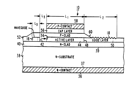
In FIGURE 2, representative device 10 will be
described with the understanding that the remaining devices
12, 14 and so forth of the array 15 coupled to waveguide 16
are constructed similarly. Device 10 comprises an N contact
36, such as sintered Ni/Ge/Ti/Au, deposited on one broad
planar surface 37 of substrate 38. Substrate 38 may be
GaAs, of N conductivity type, and a thickness of about 200N
(micrometers). Over a second planar broad surface 39 of
the substrate 38 is a first cladding layer 40 which is of N
conductivity type. The cladding layer 40 may comprise
AlxGa1_xAs where x preferably is~about 0.3. The cladding
layer 40 may have a thickness of 0.5N. Overlying the
cladding layer 40 is waveguide 16 which may have a thickness
of 0.2N and a transverse width L3 of 2N. The waveguide 16
may comprise AlyGal-yAs where y is preferably about 0.15.
waveguide 16, FIGURE 1, has a corrugated edge
formed with corrugations 42 for emitting light along optical
axis 28 to the device 10. The corrugations 42 are
constructed such that the light emitted therefrom is parallel
to axis 28. The corrugations 42 extend in a direction
parallel to the waveguide 16 axis 30 for a length sufficient
to provide optical coupling along the width of the device
10, dimension L~. Dimension L4 may have a value of about
100N. The peaks of the corrugations 42 may be spaced from
the device 10 end 34 a distance LS generally of about O.1N.
Overlying the cladding layer 40 spaced distance
LS from the waveguide 16, FIGURE 2, is active layer 44.
Active layer 44 may comprise non-doped~GaAs having a
thickness- of 0.2N. The layer 44 has a length L1 generally
of about 200-SOON. It is to be understood that this length
CA 02012229 1997-08-14
RD 18,15?P
is different across the width dimension L4 due to the angles
B and 61 of the respective ends 34 and 48 of the active layer
to a normal to axis 28. The length L1 of the active layer
therefore is a nominal value. Guide layer 50 abuts and is
optically coupled to end 48 of active layer 44 and overlies
cladding layer 40. Guide layer 50 is the same thickness as
active layer 48 and of the same transverse width dimension
L4. Guide layer 50 may comprise the same material as that
of the waveguide I6. Overlying the first cladding layer
40, waveguide 16 and active layer 44 is a second cladding
layer 52. Cladding layer 52 is of P-conductivity and
comprises Alx GaI-x As. The P-cladding layer near the
grating area gradually thins at transition region 60. This
provides effective coupling of the active region to the
guide region. Grating 18 is directly on the surface of
guide layer 50. The grating 18 is oriented at angle 6
(FIGURE 1) relative to the optical axis 28 of the active
layer 44. The elements of the- grating 18 are linear and
parallel.
A cap layer 56 is over the cladding layer 52 in
the region of active layer 44. Cap layer 56 is P-
conductivity GaAs. A P-contact 58 overlies cap layer 56.
The P-contact 58 may comprise successive layers of Ti/Pt/Au,
with the Ti layer next to the layer 56. The length
dimension LZ (FIGURE 2) of the grating may be about 50-100N.
The grating 18 has a peak-to-valley amplitude of about 0.05N.
The device of this embodiment can be made by an
epitaxial process with appropriate reagents and doping.
Grating 18 is formed by etching the guide layer 50.
In FIGURE 3, the beam 22 emitted by device 10 has
an optical axis 62. Axis 62 is tilted angle ~ which is a
function of angle a of the tilt of the grating relative to
the optical axis 28. The relationship of the angles 6 and
will now be discussed with reference made to FIGURES 4,
5, and 6. In FIGURE 5, in a conventional grating radiator
having grating elements normal to optical axis 502 (when
9=0), the periodicity n of the grating is the same as that
of wavelength ~ of the guided wave such that radiation is
CA 02012229 1997-08-14
-8- RD 18, 1»P
emitted normal to the surface. A large portion of the
guided wave is also reflected back to the guide because the
Bragg condition is satisfied. Therefore, a grating whose
corrugations are parallel to the propagation wavefront
cannot be used as an output or input coupler to an amplifier
because of the oscillations and their effect, as discussed
above. This type of grating is used for surface emission
DBR lasers because it requires strong reflections from the
grating to the active region.
However, it can be shown that the Bragg reflection
tends to.be significantly reduced when the periodicity of a
non-tilted grating is slightly different from the above
condition, i.e., not equal to that of wavelength ~. However,
reflections from the grating region are present because the
average thickness of the layer where the grating is formed
is less than the thickness of the remaining portion of the
clad layer 52 (FIGURE 1) with no grating because the grating
is etched from layer 52. The reflections are weaker than
Bragg reflections but reflections are present, e.g., 10°/,
and this. reflectivity limits the amplifier gain.
In FIGURE S, grating 500 having linear parallel
grating elements eo-en is tilted at angle a relative to a
normal to the light propagation axis 502. 6 has a value
which does not satisfy the Bragg condition and exhibits a
weaker reflection. The reflections do not reflect parallel
to axis 502 into the.amplifier region 504 because of the
angle y of the reflections. The periodicity of the grating
500 in a direction perpendicular to the grating elements is
nl and the periodicity in the wave propagation direction is
,v which is nl/cos9 and is larger than n1. The wave 507 of
wavelength J~ in the gain region propagates parallel to the
optical axis and is chosen so as to be equal to n. The
phase of the reflections 503, 504...505n from each respective
grating element eo-eN is expressed as a vector and each
reflection signal is given by:
CA 02012229 1997-08-14
-9- RD 1$,i7P
ro - sin(wt - ~ ) ( i )
at the initial grating element eo;
ri - sin(wt - (m + 2n + 2n cos 28 ) ) ( 2 )
at element ei;
r2 - sin(wt - ( ~ + 2 . 2n + 2 . 2,-c cos 2A ) ) ( 3 )
at element e2; and
rN = sin(wt - (m + 2Nn + 2Nn cos 28))
at element eN.
The term 2Nn is the path length in the grating region
before the wave is reflected and the term 2Nn cos 2B is the
path length to line A. Each pair of adjacent vectors (rN
and rN-1 or rN and rN+1) are radially spaced the same angle
2n cos 26, FIGURE 6. The summation of
rNN~OrN
becomes zero for any value of tilt angle 6 except for
A - 45°, where Bragg reflection occurs.
The angle of the radiation reflected from a
tilted grating can be calculated employing wave vectors.
As seen in FIG. 4, the incident wave vector Ki (=2n/~)
parallel to axis 502 (FIGURE 5) and the grating vector kg
(=2n/nl) normal to the grating lines, (FIGURE 5), satisfy
kg cos 26=ki and the resultant vector Kt is equal to kg-ki.
If Kt <ko (ko is the wave vector to outer space corresponding
to beam 22, FIGURE 1), radiation into the ambient atmosphere
takes place and the angle ~ is found from the relation ko
sin ~ = ki tan B.
At a very large driving current applied to a
single spatial mode stripe laser, the device temperature and
carrier temperature increase which leads to carrier leakage
from the energy barrier of a double heterostructure.. Other
kinds of problems include formation of a defect or dark
lines inside of the junction or catastrophic damages on a
CA 02012229 1997-08-14
'1Q' RD 18,157P
laser facet. All of these are caused by high energy densit-_.~
at high power level. If the stripe width is increased in
order to reduce the power density, the laser cannot be
operated in a single mode condition.
In the case of an amplifier, a large width
(dimension L4, FIGURE 1) amplifying. region does not cause
multimode operation if excitation is in a single spatial
mode. However, a suitable method of coupling from a signle
spatial mode laser to wide width amplifier is necessary.
This may be done using an integrated lens (not shown) which
converts a diverging beam from a laser to a parallel beam
on a surface wqveguide, or phased array laser (not shown)
may be directly coupled to a wide width amplifier. A
preferred arrangement is to provide a phase grating, such
as corrugation 42 (FIGURE 1), at a side of a narrow width
waveguide such as waveguide 16, (FIGURE 1), so that the
propagating wave in the narrow waveguide 16 radiates into a
relatively wide width amplifying region tilted relative to
the narrow waveguide as shown, by way of example.
In FIGURE 7, to minimize the angle 8, axis 28 is
oriented at angle ei relative to a normal to the device end
34 receiving the beam from the waveguide 16. By employing
reflections of light from the boundary 32 between the active
layer 44 and remaining semiconductor material, for example,
the P cladding layer 52, light may be reflected from the
grating region through end 48 ray 700, to the boundary 32
and reflected from the boundary to end 34 ray 702.
It can be shown that when ray 702 is reflected
from end 34 it creates ray 704 which is incident upon the
boundary 32 at an angle a greater than the critical angle
6c for the total reflection and is refracted through
boundary 32. Assume the angle a exceeds a certain value
such that the angle of incidence of the reflections from
the gratings, e.g., ray 700, are incident on the boundary
32 at a value greater than the angle 9c. It is believed
here that the grating 18 may be tilted at such a large
angle that ~ would cause the rays of the beam 22 to be
tilted more than desired, i.e., unacceptably tilted. If
CA 02012229 1997-08-14
-11- R.D 18 ( 15 7 P .
the angle 26 at which the ray 700 reflected from the
grating is smaller than the angle e~, then the rays 700 wi'i
completely reflect from the boundary 32 and be incident
upon end 34. These rays are then reflected from end 34 at
angle b and impinge upon boundary 32 at angle a. By making
the angle a somewhat greater than the critical angle ac,
then the ray 704 incident on boundary 32 from end 34 is
refracted out of the active layer 44. This action tends to
reduce the possibility of internal oscillations in the
amplifier.
Light incident on a boundary of materials of
different indices of refraction at less than the critical
angle 9c is totally reflected internally. Light incident
on the boundary at a value greater than the critical angle
is mostly transmitted through the boundary with relative
increasing transmission through the boundary proportional
to the increase of the incident angle greater than the
critical angle. The angle 6c is determined by the effective
index of refraction of the active layer 44 to the effective
index of refraction of the boundary material, cladding 52.
The effective refractive index of the active layer is a
function of the thickness of the active layer and also of
the external material at the boundry. The differences in
effective index of refractions serve as a boundary which
25) tend to confine radiation within the active layer 44 of the
device, providing total internal reflection which is
undesirable in the amplifier of the present invention.
Therefore, the angle a and the angle el have such combined
values that a is greater than the critical angle 9c and
thus, greater than 26, to prevent reflections in the active
layer 44. The critical angle a is determined as follows:
9c= cos 1(n2/nI) (5)
where nl is the effective refractive index of the active
layer 44 for 0.2N thick GaAs and is typically 3.496 and n2
is the effective refractive index of the adjacent cladding
CA 02012229 1997-08-14
-12- RD 18,15;P
52 typically 3.4 for A1Q.3Gao.~As, and 6c = 13.5°. The
angles 2B or a should be greater than 6c. when 26=ec, the
tilt angle of the radiation ~ becomes 24.3°.
In operation, in FIGURE 2, a positive voltage is
S applied to the P contact 58 and a negative voltage to the N
contact 36. Holes are injected from the P contact 58 into
the active layer 44 with cladding layer 40 providing a
barrier against further movement by the holes. Similarly,
electrons are injected from the N contact 36 into the
active layer 44. At a threshold current, population
inversion occurs and, therefore, the incident light beam is
amplified by the stimulated emission of photons. Photons
generated in the active layer 44 are emitted to the
guidelayer 50 and are incident on the second order grating
18. The photons are emitted as beam 22 non-perpendicular
to the guidelayer 50.
Because of the reduction of the reflections under
practical limitations as illustrated above in connection
with FIGURE 7, device 10 operates as an amplifier. If the
beam 22 can be closer to parallel to~the plane of grating
18, then the angle a may be made that value at which the
value 2B is greater than the critical angle 6c. In this
case, end 34 need not be made an angle 91 less than 90° to
the optical axis 28 from the above discussions as there
will be negligible reflections to and from end 34.
Normally, however, adjacent optical devices in an optical
computer, for example, require the output from the grating
to be as close to normal to the grating surface as possible.
Therefore, the angle a should be kept as small as possible
for this purpose. Generally, the angle a may be about 10°
for this purpose.
There is another advantage of having el <90°.
The light radiated from the grating 18 goes through some
optical component such as lenses and is finally fed to a
detector. From these components, external reflections may
return to the grating 18 and coupled to the amplifier. If
these externally caused reflections reach the end 34 which
is otherwise normal to the axis 28 (91 - 0~, these
CA 02012229 1997-08-14
-13- RD 18,157P
reflections from end 34 are amplified and the llg t
oscillates in the amplifier. If the- gain of the amplifier
is sufficiently high, these type of reflections cause
spurious oscillations. Thus, the tilted angle (61 <90) of
S the end 34 has a second function.
FIGURE 8 illustrates a second embodiment of the
present invention. A coupling between single mode fibers
in waveguide amplifiers has the same problem as the coupling
efficiency and alignment tolerance of a laser fiber coupling.
The device of FIGURE 8 addresses these coupling problems.
Device 800 includes amplifier 804 disposed in a semiconductor
body 802. The amplifier 804 may be constructed similarly
as device 10, FIGURES 1 and 2. The active region of the
amplifier is sandwiched between two clad regions
corresponding to the clad layers 40 and 52, FIGURE 2, with
gratings located at both ends. These layered structures
are not shown but it is assumed that the construction of
the waveguide layer, active layer, grating layer and cladding
layers are similarly reproduced in the embodiments of FIGURES
8 and 9.
Amplifier 804 is of a given desired length with
the gratings 806 and 808 at opposite ends of the waveguide
804. The gratings 806 and 808 are formed directly on the
guide layer 50 as discussed above in connection with the
embodiment of FIGURE 2. The grating elements of the gratings
806 and 808 are tilted relative to the optical axis 808 in
a manner similar to the tilt of grating 18 to axis 28. The
angle of tilt may be the angle a as discussed above in
connection with FIGURE 7.
Device 800 further includes two optical fibers
812 and 812'. Fiber 812 has a core 814 and fiber 812' has
a core 814'. The core 814 is over grating 808 and coupled
thereto and core 814' is over grating 806 and coupled
thereto. Fiber 812 may serve, for example, as an input of
an optical signal to the device 800 and the fiber 812' may
serve as an output for the device signal transmitted by the
device 800 from grating 808 to grating 806 in the direction
. of arrow 815. Ends 818 and 820 of the amplifier 804 are
CA 02012229 1997-08-14
-14- RD 18,i57P
tilted so that they are not perpendicular to the waveguide
804 optical axis 810. The tilt angle of the ends 818 and
920 may be the same value so that both gratings are parallel
and the angles of the fibers are the same for both. This
S makes the structure simpler to manufacture. The angle of
the gratings 818 and 820 to the optical axis 810 should
have a value such that the reflections at the interface
between the waveguide 804 and the adjacent material body
(clad) are at an angle greater than the critical angle 9c.
The tilt angle is such that twice the angle of tilt is by
some value greater than the critical angle 6c. Angle 9 of .
the gratings will cause the beam emitted from the emission
grating 8.06 and the beam received by the receiving grating
808 to be an angle tilted from the.perpendicular to the
plane of the surface of the gratings. This tilt, angle m',
FIGURE 9, can be estimated exactly the same way as for the
angle m, FIGURES 3 and 4. The optical fiber 812 and its
core 814 are also tilted at angle m' to transmit the beam
to grating 808.
Fiber 812, which is representative, has an end
face 822, FIGURE 9, which is polished at an angle m' to the
fiber optical axis 815. The light propagation axis 815 of
the fiber 812 is parallel to the light reception (or
emission) axis of the beam to grating 808 in the direction
of arrow 824. The light propagating in the grating region
is converted to radiation due to the effect of the grating.
The widths of the amplifier and the coupling
region are equal to the size of a single mode fiber core
and the length of the coupling region relates to the fiber
core diameter so that an angle polished fiber or cleaved
fiber can be directly coupled without lenses. Direct
coupling has a higher. coupling efficiency than a lensed
fiber. As near field patterns of .the radiator and the fiber
agree, coupling efficiency becomes 100% from overlap
integration theory.
It is important that reflections between the
gratings 806 and 808 along the waveguide 804 are reduced as
much as possible within an acceptable range of the tilt of
CA 02012229 1997-08-14
-15- RD 18,15~P
the coupled in or out beams. Therefore, the angle a becomes
important to eliminate or otherwise minimize the reflections
as discussed above. If necessary, the ends 818 and 820 may
be made at angles different than each other for an acceptable
tilt of the fibers as already discussed. Further, while
the gratings 806 and 808 are discussed as having a common
tilt angle e, it should be recognized in certain
implementations they may have different tilt angles dependi:g
on the reflection characteristics and the angles of the
coupled fibers at the emission and receiving gratings. The
important consideration is that the reflections internal in
the waveguide including an amplifier are minimized to
maximize amplifier gain.