Note: Descriptions are shown in the official language in which they were submitted.
1 - 201 231 8
MICROPROCESSOR SYSTEM HAVING AN
~ :N~ED ADDRESS SPACE
BACKGROUND OF THE INVENTION
l. Field of the Invention
The present invention relates to a micro-
processor system having an extended address space, and
particularly to an address extending technique for a
microprocessor system.
Microprocessors are easy to use, have a good
cost performance, and therefore, are frequently employed
in electronic controllers such as trunks or other
equipment in an electronic exchange system. Such a
microprocessor as mentioned above is, for example, an
eight-bit microprocessor. They have, however, only a
64-kilobyte basic address space, which is not sufficient
to store a large program for providing complicated
functions. To solve this problem, an extension of the
address space has been developed. Instead of the
eight-bit microprocessor, a sixteen-bit microprocessor
may be employed to provide a required address space.
This, however, enlarges the circuitry and adversely
affects the cost performance.
2. Description of the Related Arts
Cross references related to the present
invention are: Japanese Patent Publication (Kokai)
No. 62-25348 and Japanese Patent Publication (Kokai)
No. 62-25348.
A conventional address space extending
technique provides a basic address space with an
extended address space that supplants a part of the
basic address space. For example, the eight-bit
microprocessor has a basic address space ranging from
0000 to FFFF, and for instance, a region of 8000 to 9FFF
in the basic address space is supplanted by an extended
address space ranging from 0000 to 8000. In this case,
- - 2 - 201 231 8
a basic memory is not provided for the region of 8000 to
9FFF of the basic address space, and instead a memory
having a required capacity such as 8 kilobytes or
smaller, is provided for the extended address space.
This is possible when memory chips each having a memory
capacity of 8 kilobytes are employed.
In recent years, however memory capacity has
been increased greatly. Memory chips are no longer
limited to a capacity of eight kilobytes (64 kilobits),
but now comprise 32 kilobytes (256 kilobits) or larger.
With such memories having a large capacity, e.g., a
basic address space of, for example, 64 kilobytes may be
filled by only two of 32-kilobyte RAM and ROM memory
chips. Therefore, even when a part of one memory chip
is to be supplanted by an extended address space, the
whole space of the memory chip should be supplanted.
It may be possible to return to an address of
the original 32-kilobyte memory chip after the extended
address space has been used. This, however, requires a
complex program including the steps to return to the
original address space, resulting in a long processing
time and a large memory space for the program.
Further, according to the conventional technique
explained above, the part of the basic address space,
8000 to 9FFF, for example, supplanted by the extended
address space may be a wasted space that is never used.
SUMMARY OF THE INVENTION
An object of the present invention is to provide a
microprocessor system having an extended address space
in which the part of a basic address space supplanted by
the extended address space is used effectively with a
short processing time and a small memory space for the
program to return from the extended address space to the
original address space.
To attain the above object, there is provided,
according to the present invention, microprocessor
system for extending an address space, comprising: a
20 1 23 1 8
-- 3 --
basic memory having a first address space for storing at
least one program and a second address space or storing
data; an extended memory having an extended address
space used in place of a part of the first address
space, for storing at least one additional program; an
address extending hard register for storing a flag and
extending addresses of the extended memory, the flag
indicating which part of the first address space and the
extended address space is to be used, and the extending
addresses being used to designate the extended memory
when the flag indicates that the extended address space
is to be used; and a microprocessor, operatively
connected to the basic memory, to the extended memory,
and to the address extending hard register, for
generating an address signal and for processing data,
the address signal designating either one of the basic
memory and the extending hard register.
The program stored in the part of the first address
space is transferred by the microprocessor to the second
address space when the flag indicates that the part of
the first address space is to be used; and the extending
addresses are used to designate the extended memory when
the flag indicates that the extended address space is to
be used and when the address signal from the micro-
processor designates the part of the first address
space.
BRIEF DESCRIPTION OF THE DRAWINGS
The above objects and features of the present
invention will be more apparent from the following
description of the preferred embodiment with reference
to the drawings, wherein:
Figure l is an address map for explaining a
principle of an embodiment of the present invention;
Figure 2 is a view showing an address
extending register according to an embodiment of the
present invention;
Figures 3A to 3C are block diagrams showing a
~ _ 4 _ 2012318
microprocessor system according to an embodiment of the
present invention;
Figure 4 is an address map according to an
embodiment of the present invention;
Figure 5 is a view showing the address
extending register according to an embodiment of the
present invention;
Figure 6 is a flowchart showing a system
start-up process according to an embodiment of the
present invention; and
Figure 7 is a flowchart showing an extended
space using process according to an embodiment of the
present invention.
DESCRIPTION OF THE PREFERRED EMBODIMENTS
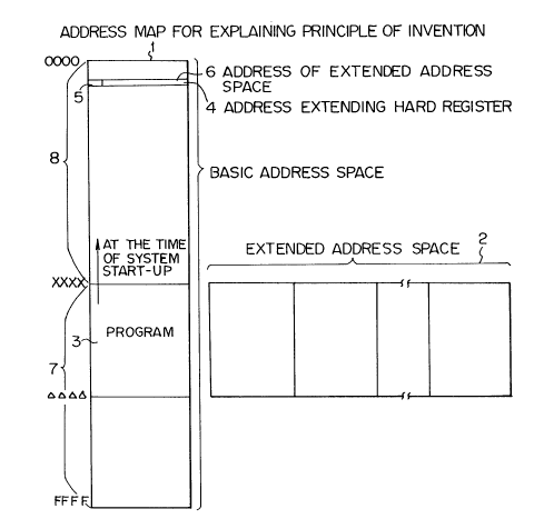
Figure l is an address map for explaining a
principle of an embodiment of the present invention. In
the figure, numeral l denotes a basic address space
(0000 to FFFF) for storing basic programs and data used
by a microprocessor; 2 an extended address space used by
the microprocessor in place of a part 3 txxxx to
of the basic address space l and storing extended
programs; 4 an address extending hard register; 5 a flag
for indicating which of the part 3 of the basic address
space l and the extended address space 2 is used; and 6
an address of the extended address space 2.
The basic programs and fixed data are stored in a
program storing region 7 realized by, for example, a
read only memory (ROM) chip, and the data is stored in a
data storing region 8 realized by, for example, a random
access memory (RAM) chip.
Before starting up the system, the data storing
region 8 is empty.
The part 3 of the basic address space l stores
programs, which are transferred to a data storing region
of the basic address space l at the time of system
start-up, i.e., during an initial program load Gf the
system.
- 5 - 20 1 23 1 ~
- At the start-up of the system, the flag 5 of the
address extending hard register 4 is set to "1" to
transfer the program data stored in the part 3 to a data
storing region 8 of the basic address space 1. To use
the extended address space 2, the flag 5 of the address
extending hard register 4 is set to "0", and a block of
the extended address space 2 to be used is specified by
an address held in the address extending hard
register 4. With this arrangement, the data stored in
the part 3 ranging from xxxx to ~ of the basic
address space 1 is effectively used, and the part 3 can
be switched to the extended address space 2 after the
start-up of the system. When the program is stored in
the address space ranging from ~ to FFFF, the process
automatically goes to that space without any specific
instruction to move from the extended address space 2 to
that address space between ~ and FFFF.
Figure 2 shows an arrangement of an address
extending hard register according to an embodiment of
the present invention. In the figure, the address
extending hard register 4 is an eight-bit register
having bits EXA0 through EXA6 and EXEN. The bit 7
(EXEN) specifies which of a basic address space and an
extended address space is used, and the bits 0 through 6
specify an address of the extended address space. The
address extending hard register 4 is placed, as an
example, on the address 0400 of the data storing
region 8.
Figures 3A to 3C are block circuit diagrams showing
a part of an eight-bit microprocessor system according
to an embodiment of the present invention. In the
figures, numeral 11 denotes an eight-bit microprocessor;
12a a RAM having a capacity of 256 kilobits
(32 kilobytes) for storing data in the basic address
space; 12b a ROM having a capacity of 256 kilobits
(32 kilobytes) storing programs and fixed data in the
basic address space; 13 a ROM having a capacity of
- 6 - 2 0 l2 3l8
256 kilobits arranged for the extended address space; 14
the address extending hard register; 15 a NAND gate
circuit; 16 a NOT gate circuit; 17 a NAND gate circuit;
18 a NOR gate circuit; 19 a NOT gate circuit; 20 an
OR gate circuit; 21 a NAND gate circuit; and 22 an
address decoder.
The microprocessor 11 generates a 16-bit address A0
through A15, 8-bit data D0 through D7, an enable
signal E, and a read/write signal RW.
Whether or not an address space is extended is
determined by the value of an output 8Q (corresponding
to the flag 5 of Fig. 1 and the bit 7 (EXEN) in Fig. 2)
of the address extending hard register 14, and the
values of higher order address outputs A13, A14, and A15
of the microprocessor 11.
Combinations of the values of the outputs A13, A14,
Al5 of the microprocessor 11 and the output 8Q of the
address extending hard register 14 will be explained
next.
(1) At the time of system start-up, the
address extending hard register 14 is reset so that the
output 8Q (*7) thereof is set to "1".
In this state, even when the highest
order address signal A15 is "l", the basic ROM 12b is
selected and the extended address space ROM 13 is not
selected. This is because, when the bit 8Q is "1", the
inverted output of the NOR gate 18 is "0" regardless of
the values of the address outputs Al3 and A14 applied to
the inputs of the NOR gate 18, accordingly, if the
address output A15 is "1," an output of the NOT gate
circuit 19 is "0, and an output (*4) of the OR gate
circuit 20 is "0," which is provided to an inverting
chip enable terminal CE of the basic ROM 126, thereby
selecting the basic address space ROM 126. Meanwhile,
an output (*6) of the NAND gate circuit 21 is "l," which
is provided to an inverting chip enable terminal CE of
the extended ROM 13, thereby not selecting the extended
- 2~231~
address space ROM 13. The address output A15 of the
microprocessor 11 is also applied through a line *15 to
an inverting first chip enable terminal CE1 of the
RAM 12a so that it is not selected.
The operation of moving programs from a
part of the ROM 12b to a part of the RAM 12a at the time
of system start-up (during the initial program load of
the microprocessor) is carried out byte by byte.
Namely, the programs stored in the address space of, for
example, 8000 to 9FFF are transferred to a part of the
RAM 12a. To this end, first, the enable signal E in the
microprocessor ll is set to "1" and the read/write
signal RW is set to a read signal ("1"). The read
signal passes through the NAND gate 15 so that its
output becomes "0" which is applied through a line *1 to
the inverting output enable terminals OE of the RAM 12a,
the ROM 12b, and the extended ROM 13. Then, by
generating an appropriate address to designate an
address in the range from 8000 to 9FFF of the ROM 12b,
one byte of data is read. Next, the read/write signal
is changed to a write signal ("0"). By generating an
appropriate address to designate an address in the
RAM 12a, the programs read from the ROM 12b are written
in the RAM 12a. By repeating the above operation, the
programs in the range from 8000 to 9FFF in the ROM 12b
are moved to the RAM 12a at the time of system start-up.
(2) The ROM 12b stores an instruction to
change the output 8Q from "1" to "0".
When the output 8Q of the address
extending hard register 14 is "0,'~ when the address
outputs A13 and A14 of the eight-bit microprocessor 11
are each "1," and when the address output A15 of the
microprocessor 11 is "1,' then the inverted output of
- the NOR gate circuit 18 is "1," and therefore, an
output (*4) of the OR gate circuit 20 is "1," thereby
not selecting the basic address space ROM 12b.
Meanwhile, an inverted output (*6) of the NAND gate
- 8 2 0 1 2 3 1 ~
circuit 21 is "0," which is applied to an inverting chip
enable terminal CE of the extended address space ROM 13
thereby selecting the extended address space ROM 13. At
this time, the values of outputs lQ and 2Q of the
address extending hard register 14 are provided through
a line *12 to address input terminals A13 and A14 of the
extended address space ROM 13 to select one of four
eight-kilobyte blocks of the extended address
space ROM 13.
In this way, the addresses 8000 through
9FFF of the basic address space ROM 12b are supplanted
by the extended address space ROM 13.
(3) With the output 8Q of the address
extending hard register 14 being "0," at least one of
the address outputs A13 and A14 of the eight-bit
microprocessor 11 being "1," and the address output A15
of the microprocessor 11 being "1," the inverted output
of the NOR gate circuit 18 is "0" and the output of the
OR gate circuit 20 is "0," thereby selecting the basic
address space ROM 12b. Namely, when the address
generated by the microprocessor 11 is over 9FFF, the
ROM 12b is automatically selected without any specific
instruction to return from the extended area to the
ROM 12b. Meanwhile, the inverted output of the NAND
gate circuit 21 is "1," thereby not selecting the
extended address space ROM 13.
The address decoder 22 is enabled when
the RAM 12a is selected. Namely, with the address
outputs A13, A14, and A15 of the eight-bit micro-
processor 11 through lines *9 and *10 each being "0" the
3-bit outputs A10 through A12 through a bus line *8 from
the eight-bit microprocessor 11 are decoded by the
address decoder 22. When the 3-bit addresses A10
through A12 are 100, the output (Yl) 1 is selected so
that the address extending hard register 14 is enabled.
Namely, the address extending hard register 14 is
enabled when the eight-bit microprocessor 11 provides an
20 1 2~ 1 ~
g
output address of 0400 in hexadecimal expression, or
0000 0100 0000 0000 in binary expression. This value,
however, is not limited to 0400, and any value in a RAM
region is acceptable.
Figure 4 is an address map of the system
of Fig. 3. In Fig. 4, the basic address space ranges
from 0000 to FFFF. The address extending hard
register 14 is the flip flop shown in Fig. 3 and is
positioned at an address 0400. The RAM area extends
from 0000 to 7FFF including the address extending hard
register region. In this embodiment, the part of the
basic address space that is supplanted by the extended
address space ranges from 8000 to 9FFF. The extended
address space ROM comprises four blocks EX0, EXl, EX2,
and EX3 having address spaces 0000 through lFFF, 2000
through 3FFF, 4000 through 5FFF, and 6000 through 8FFF,
respectively.
Figure 5 shows an arrangement of the
address extending hard register 14 according to the
embodiment of the present invention. In the figure, the
address extending hard register 14 is an eight-bit
register having bits 0 (lQ) through 7 (8Q). The bits
0 (lQ) and 1 (2Q) specify one of the blocks of the
extended address space, and the bit 7 (8Q) specifies the
basic address space or the extended address space.
Namely, the bit 7 (EXEN) of "1" specifies the basic
address space, and "0" the extended address space. A
combination of the bits 0 ( IMA0 ) and 1 (IMAl) of "00"
specifies the block EX0, "10" the block EX1, "01" the
block EX2, and "11" the block EX3.
Figure 6 is a flowchart showing a system
start-up process. When the system is started up, the
flag EXEN of the address extending hard register 14 is
set to "1" to specify the basic address space. The data
at the addresses 8000 through 9FFF of the basic address
space are transferred to the RAM region ranging-from
0000 through 7FFF. The flag EXEN is then set to "0."
- lO - 201231~
Thereafter, when an address in the range from 8000 to
9FFF is accessed, the extended space is used. In
addition the program data stored at the addresses 8000
through 9FFF of the basic address space are used
effectively.
Figure 7 is a flowchart showing an
extended space using a process according to the
embodiment of the present invention. During a usual
operation except for the system start-up operation, any
of the blocks EX0 to EX3 of the extended address space
may be specified, and after any one is specified, a
reading or writing access to the addresses 8000 through
9FFF may be carried out to the specified block.
As explained above, at the time of system
start-up, a common program sets the bit 7 of the address
extending hard register 14 to "1" transfer the program
data stored in the part of the basic address space to
the RAM region of the basic address space. After that,
the bit 7 of the address extending hard register 14 is
set to "0," so that, by only setting the bits 0 and 1 of
the address extending hard register 14 as required, a
program can freely use the basic space of addresses A000
through FFFF and the extended space. The invention can
therefore improve the performance of the system without
complicating the programs.
As apparent from the above explanation,
the present invention provides a microprocessor system
having an extended address space that supplants a part
of a basic address space. Program data stored in the
part of the basic address space to be supplanted is
transferred to a RAM region of the basic address space
at the time of system start-up. Accordingly, the part
of the basic address space to be supplanted can be used
effectively, and therefore, the system can store a large
amount of programs, thereby improving the performance of
the system.