Note: Descriptions are shown in the official language in which they were submitted.
1 FJ-7762
ZOlZ39Z
., -- 1 --
VARIABLE TRANSMISSION POWER TYPE TRANSMITTER
BACKGROUND OF THE INVENTION
1. Field of the Invention
The present invention relates to a variable
transmission power type transmitter comprising a
transmission interruption detecting circuit.
2. Description of the Related Art
In a mobile communication system such as an
automobile telephone system, a portable telephone
system, and the like, in order to prevent a mobile
terminal from transmitting needlessly, and to reduce
power consumption of the mobile terminal, the
transmission power of the mobile terminal is controlled
to be kept as low as possible while maintaining
communication when electrical field strength is
sufficiently high at the mobile terminal's position, and
the transmission power is turned off when transmission
is not required.
In order to realize these functions, a radio
transmitter for a base station and a mobile terminal are
provided with an automatic power control circuit (APC
circuit) which is capable of variable control of the
transmission power. The radio transmitter is also
provided with a transmission interruption detecting
circuit (or CAR-IND circuit: carrier indicator) for
detecting existence or absence of the transmission
output, in cooperation with the automatic power control
circuit. The radio transmitter is further provided with
a set point providing circuit for providing the
automatic power control circuit with a set point by
which the transmission power of the automatic power
control circuit is controlled. The set point providing
circuit discretely alters the value of the set point
between the values corresponding to a m;nimum power Pmin
and m~x;mum power PmaX , according to a command issued
from a processor to control the whole apparatus.
~a~
~`
2$12392
The transmission interruption detecting circuit compares a
detected value of a level of the transmitting power with a
predetermined reference value Vref to decide whether the
transmission power exists or not. The reference value Vref is
manually adjustable to compensate for dispersion of each element.
The values corresponding to the Pmjn and P~x are also manually
adjustable for compensation.
In the aforementioned conventional circuit, adjustment of
the reference value Vref is required after adjustment of the
values corresponding to the PmaX and the Pmjn. Accordingly, there
are so many portions to be adjusted that several production pro-
cesses are required. Additionally, the scale of the circuit is
large and its price is high, since a variable resistor for
adjustment of the reference value Vref is required.
SUMMARY OF THE INVENTION
It is a feature of one embodiment of the present invention
to provide a variable transmission power type transmitter which
can be made small in size and at low cost and which can be
produced using a simple process without need for adjustment of
the reference value Vref.
In accordance with an embodiment of the present invention
there is provided a variable transmission power type transmitter,
comprising: transmission amplifier means for outputting a trans-
mission wave signal having a variable transmission power at an
output side; detecting means, operatively connected to the output
side of the transmission amplifier means, for detecting the
variable transmission power of the transmission wave signal and
outputting a detected value corresponding thereto; automatic
power control means for automatic control of the variable trans-
mission power of the transmitter amplifier means based on adifference between a selected set value and the detected value
of the detecting means; set point providing means for generating
set values and for selecting one of the set values to be supplied
to the automatic power control means as the selected set value;
~,
2012392
and transmission interruption detecting means for detecting
existence or absence of the transmission wave signal by comparing
the detected value of the detecting means with a reference value
generated from one of the set values in the set point providing
means.
In accordance with another embodiment of the present inven-
tion there is provided a variable transmission power type trans-
mitter, comprising: transmission amplifier means for receiving
an RF signal at an input side and for outputting a transmission
wave signal having a variable transmission power at an output
side; detection means, operatively connected to the output side
of the transmission amplifier means, for producing a detected
voltage corresponding to the variable transmission power of the
transmission wave signal output from the transmission amplifier
means; power selection means for selecting one of a plurality of
power level settings as a selected power level setting and for
producing a reference voltage based on one of the plurality of
power level settings; power control means, operatively connected
to the detecting means, the power selection means and the trans-
mission amplifier means, for receiving the detected voltage from
the detection means and for automatic control of the variable
transmission power of the transmission amplifier means based on
a difference between the detected voltage and the selected power
level setting; and transmission interruption detection means,
operatively connected to the detection means and the power
selection means, for comparing the reference voltage to the
detected voltage to produce a comparison signal and for detecting
absence of the transmission wave signal at the output side of the
transmission amplifier means based on the comparison signal.
BRIEF DESCRIPTION OF THE DRAWINGS
Figure 1 is a block diagram showing an example of a mobile
terminal;
Figure 2 is a circuit diagram of a conventional transmitter
power variable transmitter;
/
2012392
- 3a -
Figure 3 is a diagram showing the characteristics of the
transmission power against the set values;
Figure 4 is a block diagram of a basic construction of the
present invention; and
Figure 5 is a circuit diagram of an embodiment of the
present invention.
DESCRIPTION OF THE PREFERRED EMBODIMENTS
Before describing the preferred embodiments according to the
invention, examples of aforementioned related art are given with
reference to the accompanying drawings.
Figure 1 shows a construction of an example of a conven-
tional mobile terminal.
A radio wave from a base station (not shown) includes
information regarding electric field strength, etc., as well as
information regarding an audio signal. A received signal inclu-
ding that information is amplified in a radio receiver 42, trans-
formed into an intermediate frequency signal in a mixer 38 which
mixes an input signal with a signal from a local oscillator 40,
divided into a signal including audio information and a signal
including information on the electrical field strength in band
pass filters 36 and 28 to pass signals having corresponding
frequencies only, respectively, and demodulated in demodulators
34 and 26, respectively.
A microprocessor 24 receives the information regarding the
electric field strength, etc., decides on an adequate transmis-
sion power, and issues a command toward a set point providing
circuit 6'. The set point
201X39Z
-- 4
providing circuit 6' selects a voltage value from among
several predetermined voltage values corresponding to
several transmission powers between PmaX and Pmin / and
supplies the selected voltage value to an automatic
power control circuit (APC circuit) 5. The automatic
power control circuit 5 and a detecting circuit 2 form a
feedback path for a power amplifier circuit 1 to be
controlled so that the level of transmission output
becomes a value corresponding to the voltage value
selected in the set point providing circuit 6'.
The microprocessor 24 also controls the ON/OFF of
the power amplifier circuit 1 through the automatic
power control circuit 5. The transmission output is
interrupted when transmission is not required.
A transmission interruption detecting circuit (or a
carrier indicator) 3' detects transmission interruption
from an output of the detecting circuit 2 and indicates
the result on an indicator (not shown).
Figure 2 shows detailed constructions of the
carrier indicator 3', the automatic power control
circuit 5, and the set point providing circuit 6' shown
in Fig. 1. The detecting circuit 2 detects the level of
the transmission wave output to output a corresponding
voltage Vl by AM detection of the transmission wave
output. The carrier indicator 3' compares the
voltage Vl with a predetermined reference voltage Vref
to decide whether the transmission power exists or not.
A variable resistor 4 is provided for correctly setting
the reference voltage Vref , compensating for dispersion
of each element. A variable resistor 7 is provided for
adjusting transmission power when minimum transmission
power P . is selected. A variable resistor 8 is
mln
provided for adjusting transmission power when maximum
transmission power PmaX is selected.
The carrier indicator 3' is constructed to include
a comparator 31 and resistors 32 to 35. The output of
the detecting circuit 2 is input to one of the input
2012392
- 5 -
terminals of the comparator 31, and the reference
voltage Vref which is a voltage divided by a resistor 32
and the variable resister 4 is input to the other input
terminal of the comparator 31.
The set point providing circuit 6' is constructed
to include a switching circuit 60 and a voltage dividing
circuit comprising eight serially connected resistors 61
to 68. Each divided voltage from the voltage dividing
circuit is input into one of the input terminals of the
switching circuit 60 as set values X0 to X7 ,
respectively. The switching circuit 60 selects one of
the set values X0 to X7 depending on a power control
signal PCont (binary signal of 3 bits) input to its
control input terminals A, B, and C, to output a set
value X on its output terminal.
The automatic power control circuit 5 is
constructed to include amplifiers 51 and 52, and driving
transistor 53 and 54, and other elements which operate
in conjunction therewith. The automatic power control
circuit 5 supplies control outputs Vddl and Vdd2 having
magnitudes depending on the set value X from the set
point providing circuit 6', to the power amplifier
circuit 1. The value of the minimum transmission power
Pmin is adjustable by a minimum value adjusting
voltage Vmin input from the m;n;~um power adjusting
variable register 7 to the amplifier 51. The
transmission wave signal from the power amplifier
circuit 1 is turned off by stopping application of a
power voltage Vcc to the transistor 54. The stopping of
the power voltage Vcc is performed in a part of the
circuit which is not shown, according to an OFF signal
from the microprocessor 24 shown in Fig. 1.
Operations of the circuits shown in Fig. 2 are
described next.
The RF signal input to the power amplifier
circuit 1 is amplified to be output as a transmission
wave signal. The transmission wave signal is AM
201239%
-- 6 --
detected in the detecting circuit 2, and the power of
the transmission wave signal currently output is
detected as a detected output Vl. The detected
output V1 is input to the carrier indicator 3' and to
the automatic power control circuit 5.
The optimum transmission power of the power
amplifier circuit 1 is decided according to the
electrical field strength. The power control
signal PCont corresponding to the decided transmission
power is input to the set point providing circuit 6'.
The set point providing circuit 6' selects a set value
corresponding to the power control signal PCont from
among the XO to X7 to be output to the automatic power
control circuit 5 as a selected set value X.
In the automatic power control circuit 5, the
amplifier 51 amplifies the result of subtraction of the
divided voltage by the variable resistor 7 from the set
value X, to output voltage V2 , the amplifier 52
amplifies the result of subtraction of the detected
output V1 from the output voltage V2 to drive the
transistor 53, and the control outputs Vdd1 , and Vdd2
are generated. The power amplifier circuit 1 is
controlled by the control outputs Vdd1 and Vdd2 so that
desired transmission power is output.
Adjustment of values of the minimum and maximum
transmission power is performed by the variable
resistor 7 for adjustment of the minimum power, and the
variable resistor 8 for adjustment of the maximum power,
respectively.
Figure 3 shows the characteristics of the
transmission power in the power amplifier 1 corre-
sponding to the set values XO to X7. The value of the
minimum transmission power Pmin corresponding to the set
value X7 can be adjusted with the variable resistor 7
for adjustment of the minimum power, and the value of
the maximum transmission power PmaX corresponding to the
set value XO can be adjusted with the variable
2012392
register 8 for adjustment of the maximum power.
The carrier indicator 3' (Fig. 2) is a circuit for
generating a signal to indicate whether the transmission wave
signal from the power amplifier circuit 1 exists or not. The
detected output V1 from the detecting circuit 2 is compared with
the reference value Vref generated in the variable resistor 4 for
adjustment of the reference value. If the detected value V1 is
lower than the reference value Vref, then the transmission wave
signal is determined not to exist. The reference value Vref is
required to be set lower than a value corresponding to the
minimum transmission power Pmjn. Generally, the reference value
Vref is set at a value corresponding to a transmission power which
is lower than the minimum transmission power Pmjn (for example,
lower than 1 mW) by more than 4 dB (Fig. 3).
In the aforementioned conventional circuits, the reference
value Vref is required to be additionally adjusted with the
variable register 4, after the maximum value PmaX and the minimum
value Pmjn of the transmission power have been adjusted with the
variable resistor 8 and the variable resistor 7, respectively.
Therefore, there are so many portions to be adjusted that pro-
duction processes are quite numerous. Additionally, the scale
of the circuits is large and their cost is high, since a variable
resistor for adjustment of the reference value Vref is required.
Figure 4 shows a basic construction of the present inven-
tion.
A transmission amplifier unit 11 outputs a transmission wave
signal having variable transmission power. A detecting unit 12
detects the transmission wave signal from the transmission
amplifier unit 11. A set point providing unit 13 generates set
values corresponding to each value of the transmission power.
An automatic power control unit 14 automatically controls the
transmission amplifier unit 11 so as to output the transmission
power corresponding to the set value of the set point providing
unit 13, referring to the detected output of the detecting unit
~ .~
2~1239~
12. The transmission interruption detecting unit 15 decides
existence or absence of the transmission wave signal by comparing
the detected output of the detecting unit 12 with a reference
value generated from a minimum set value in the set point
providing unit 13.
An adequate reference value can be automatically generated,
for example, by dividing the minimum set value. Therefore, an
adjusting unit for generating the reference value is not requi-
red, and a working process for adjustment of the reference value
is not required.
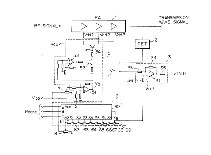
Figure 5 represents an embodiment of the present invention.
The same reference numerals as used in Fig. 2 are used for
constituents which have the same construction as those in Fig.
2. The circuits shown in Fig. 5 differ from those in Fig. 2 in
that the variable resistor 4 for adjustment of the reference
value is not used. The reference value Vref is generated by
dividing the set value X7 with serially connected resistors 68
and 69. The values of the resistors 68 and 69 are selected so
that the generated reference value coincides with a decision
point to decide the transmission interruption as shown in Fig.
3 (for example, a value lower than the set value X7 by more than
4 dB).
In this construction, the reference value Vref for the
carrier indicator 3 is automatically set when the maximum and
minimum transmission power of the power amplifier circuit 1 is
adjusted with the variable resistors 8 and 7. Accordingly, an
adjustment process of the reference value Vref is left out and the
variable resistor 4 for adjustment is not required.
The many features and advantages of the invention are
apparent from the detailed specification and thus it is intended
by the appended claims to cover all such features and advantages
of the invention which fall within the true spirit and scope
thereof. Further, since numerous modifications and changes will
readily occur to those skilled in the art, it is not desired to
-
2012392
limit the invention to the exact construction and operation
illustrated and described, and accordingly all suitable
modifications and equivalents may be resorted to as falling
within the scope of the invention.