Note: Descriptions are shown in the official language in which they were submitted.
FN 43228 CAN 2A
FIBER OPTIC DATA RINK SYSTEM
Background of the Invention
Many standards exist in the field of data
communications. There are, for example, many software
standards, or protocols, for encoding and transmitting the
data. Some of these standards provide the ability of
discovering or even correcting transmission errors.
Before the question of such software standards
can even be reached, however, choices must be made among a
myriad of hardware standards. Such hardware standards may
provide for "parallel" data transmission in which a
plurality~of data bits are transmitted simultaneously.
Usually a parallel data communications channel will provide
for the transmission of eight data bits at a time,
corresponding to an eight-bit byte. There is nothing that
inherently restricts such parallel communications to
eight-bit data channels, however, and any convenient number
of bits may be transmitted simultaneously.
Alternatively a data channel may be a serial data
channel in which a single data bit is transmitted at a
time. The data bits are then accumulated by the receiver
and assembled into the desired groupings, again typically,
although not necessarily, eight-bit bytes.
in addition to the data being transmitted most
data communication channels, both parallel and serial, will
include a number of control signals. These control signals
will allow the ports communicating with ome another to
properly utilize the communications channel to insure that
information is correctly transmitted and received.
Perhaps the best known standard for a serial
communication channel is the RS232C. The RS232C standard
specifies specific uses for each of 25 signal lines
connecting two electronic systems that are to communicate
_ 2 _
with one another. Of these 25 lines, two are for data
transmission, one in each direction, and the others are
used either to match electrical ground potentials between
the two systems or to provide control signals.
The RS232C standard is defined for communications
between two different types of devices. These are referred
to as data terminal equipment-type devices (DTE) and data
communication equipment-type devices (DCE). At times,
however, it is desirable to use an RS232C channel to cause
two devices, each of which is configured as a DTE, to
communicate with one another. Additionally, although it
makes little sense in terms of the definitions in the
standard, in the real world it is sometimes desirable to
connect two DCE devices for communication with one another.
Furthermore, even within the definitions of DTE and DCE,
there is some room for variation from one system to
another. As a result, the exact configuration of the
devices to be connected must be known in advance and
special cables and/or jumpers provided in order to permit
communication between the devices.
At times it is desirable to substitute optical
fiber for electrical wires in data communication cable.
That is because capacitance of the wires limits
transmission distance, a problem that does not exist with
optical fiber. Furthermore, in an electrically noisy
environment electrical signals on wires are subject to
degradation while optical signals are not. zn such a
system the digital state of several lines of a
communication channel, as received from a communication
Port, are multiplexed into a single data packet and
transmitted on a single fiber. This does not relieve the
operator of the requirement of advance knowledge of the
nature of the communication ports; however, because the
receiver must demultiplex the signals and send them to the
Proper line of the receiving communication port.
2~~~~~~
- 3 -
Summary of the Invention
According to the present invention apparatus is
provided for use with a fiber optic data channel. The
apparatus includes a multiplexer/transmitter for
multiplexing data into data packets and transmitting the
data packets over an optical fiber, the transmitted data
packets including configuration data packets and message
data packets. The apparatus further includes configuration
block for detecting the configuration of an associated
communication port and providing information about that
configuration to the multiplexer/transmitter for
construction of transmitted configuration data packets.
The configuration block also configures the apparatus for
proper operation with the local communication port and with
a distant communication port. The apparatus also includes
a receiver/demultiplexer for receiving data packets on an
optical fiber and demultiplexing said data packets. The
received data packets include configuration data packets
and message data packets. The receiver demultiplexer sends
data from configuration data packets to the configuration
block and data from the message data packets to the local
communication port.
Detailed Description of the Drawing
Figure 1 is a block diagram of the present
invention;
Figure 2 is a block diagram of the configuration
block of the present invention;
Figure 3 is an electrical schematic diagram of a
first circuit for detecting the configuration of a
communication port;
Figure 4 is an electrical schematic diagram of a
second circuit for detecting the configuration of a
communication port;
~~~~~~~
Figure 5 is an electrical schematic diagram of an
alternative embodiment of the second circuit for
determining the configuration of a communication port;
Figure 6 is an electrical schematic diagram of a
digital filter for use with the present invention;
Figure 7 is a block diagram of a transmitter for
use with the present invention; and
Figure 8 is a block diagram of a receiver for use
with the present invention.
Detailed Description of a Preferred Embodiment
The present invention will be described in terms
of a data communication system comprising a local
communication port and a distant communication port. Each
of the ports is capable of transmitting and receiving
information on a plurality of parallel information
channels. It will be understood, howe~~er, that the
communication ports need not be parallel ports in the
traditional sense of that term. For the purposes hereof,
communication ports capable of transmitting and receiving
parallel information will also include traditional serial
communication ports where two parallel channels are used to ,
transmit data, one for each direction of transmission or
where data is transmitted on one or more channels parallel
to control signals on other channels.
In the present invention the requirement of
having advance knowledge of the configuration of a
communication port is eliminated by providing a circuit
~ that senses that configuration. After the configuration
has been determined, information concerning it is stored in
a register and is transmitted to a similar circuit
connected to a distant communication port. A similar
circuit at the distant communication port senses the
configuration of its associated port arid stores information
concerning that configuration and transmits it back to the
original circuit. Both of the circuits then determine
- 5 - 2~~.~~~9
whether a valid connection is possible between the two
ports and automatically configure themselves for
communication.
Figure 1 is a block diagram of a data link
according to the present invention. The data link of
Figure 1 includes a transmitter 10, a receiver 12, a
configuration block 14 and a system controller 16. System
controller 16 provides control signals such as clock
signals and enable and disable signals to the other
portions of the circuit.
Configuration block 14 is shown in more detail in
Figure 2. Configuration block 14 includes configuration
detection circuitry 22, self-configuration register 24,
other configuration register 26, system configuration
register 28, and input/output controller 30.
Configuration detection circuitry 24 provides
circuitry for determining if information channels or lines
in a communication port to which it is connected are
intended to be inputs or outputs. Two strategies for
making such a determination are employed. The first is to
monitor an information channel in the communication port to
determine whether the electrical potential is changing
between digital states. If it is, the port is driving the
channel and it is an output for that port.
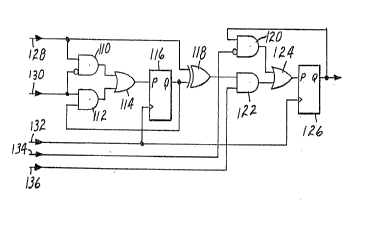
Figure 3 illustrates a circuit for so monitoring
an information channel. The circuit of Figure 3 includes
an input register comprising AND gates 110 and 112, OR gate
114 and D-Type flip-flop 116 and a difference generator and
register comprising E?cCLUSTVE-OR gate 118, AND gates 120
and 122, OR gate 124 and D-Type flip-flop 126.
There are five input signals to the circuit of
Figure 3. These signals are the data signal received from
the communication port and applied to line 128, a Hold-Not
Hold signal applied to line 130, a system clock signal
3S applied to line 32, a reset signal applied to line 134 and
a test signal applied to line 136.
-6-
Initially du ring the test sequence the Hold-Not
Hold signal on line 130 and the test signal on line 136 are
held low while the reset signal on line 139 is held high.
Since line 130 is in a low state the output AND
gate 112 will be low while the output of AND gate 110, and
thus OR gate 114 will follow the data input signal on line
128. Thus at the first clock pulse on line 132 the value
of the current data signal on line 128 will be stored in
flip-flop 116.
At the same time, since the reset signal on line
134 is held high and the test signal on line 136 is held .
low, both AND gate 120 and AND gate 122, and as a
consequence OR gate 129, will have low output signals.
Thus on the same first clock cycle a low value will be
stored in flip-flop 126.
After the system clock signal on line 132 has
been cycled causing the initial values to be stored in
flip-flop 116 and 126 as described above, the Hold-Not
Hold, reset and test signals are all inverted. Hecause the
Hold-Not Hold signal on line 130 will then be at a high
value, AND gate 110 will have a low input and thus will
have a low output regardless of the value of the data .
signal on line 128. Conversely AND gate 112 will receive a
high input signal from line 130. Thus the output of AND
gate 112 will be high if the output of flip-flop 116 is
high or low if the output of flip-flop 116 is low. OR gat a
119 will thus receive a low signal from AND gate 3.10 and
either a high or low signal from AND gate 112, the value of
the signal from AND gate 112 being the same as the output
of flip-flop 116. Thus the output of OR gate 119 will be
the same as the output of flip-flop 116. This results in
the value in flip-flop 116 remaining unchanged when
Hold-Not Hold signal on line 130 is high. y
Since the output of flip-flop 116 is latched at
the value of the data signal during the first time period,
EXCLUSIVE-OR gate 118 will always receive one input signal
equal to that initial data value during the test. The
~~1.~ ~~9
- 7 -
other input to EXCLUSIVE-OR gate 118 will be equal to the
subsequent data signals during the test. As a result, the
output of EXCLUSIVE-OR gate 118 will be equal to zero at
any time that the data signal is the same as the initial
data signal. latched in flip-flop 116 and will be high if
the data signal differs from the initial value.
Because the reset signal on line 134 is low, AND
gate 120 will receive one high input. The other input to
AND gate 120 is the output signal from flip-flop 126.
Since flip-flop 126 was reset to a low output value, this
signal will initially be low. Therefore, the output of AND
gate 120 will initially be low. 'Phe test signal on line
136 is high, giving AND gate 122 a high input. Therefore,
the output signal from AND gate 122 will equal the output
signal from EXCLUSIVE-OR gate 118. Thus, AND gate 122 will
have a high output if a difference between the initial data
signal latched in flip-flop 116 and a subsequent data
signal on line 128 is detected and low otherwise. If such
a difference is detected, OR gate 124 will receive a high
input signal and will be then provide a high output signal.
On the next cycle of the clock signal on line 132 that high
signal will be latched into flip-flop 126. Thereafter, the
output of flip-flop 126 will be high. That high signal
will be fed back to AND gate'1'20, which thereafter will
have two high signals, insuring that OR gate 124 will
always receive at least one high input signal. Thus, the
output of flip-flop 126 will be guaranteed to remain high
until the system is reset to begin the detection pro;.ess
again.
If the output signal from flip-flop 126 is high,
the signal on data input line 128 has changed digital
states. For this to be true, data input line 128 must be
connected to an output line on the communication port to
which the circuit is attached. Since the line is known to
be an output, the self-configuration circuitry may proceed
with the configuration procsss: If the outpu signal from
flip-flop 126 is low, however, there is no assurance that
~~3~,~~~~
-s-
the line of the port to which data in line 128 of the
present circuit is connected is an input line. The
possibility remains that it could be an output line that
has not changed digital states during the time of the test.
If the test of the circuit of Figure 3 is unable
to conclusively determine that line 128 is connected to an
output of the communication port to which the circuit is
connected, a different test strategy may be employed. A
circuit for the alternative test strategy is provided in
Figure 4. The strategy of the circuit of Figure 4 is based
on a difference between an output line and an input line in
a communications port.
If a particular line is an output line, it will
have connected to it a driver intended to hold the line at
a particular voltage indicative of the current logic state.
If, however, the line of the port to which line 128 is
connected is an input, the circuitry in the port will be
intended to since the voltage imposed by an outside source.
The strategy of the circuit of Figure 4, thus, is to
attempt to drive line 128 alternately to the high and low
voltage states and monitor what its voltage is. Driver 144
and resistor 146 are chosen such that they will easily
drive line 128 to the desired voltage if line 128 is
connected to an input of the port, but will be overcome by
the effect of a typical driver in an output line of a
communications port. Thus if line 128 is at a high voltage
level while driver 144 is attempting to drive it to the low
voltage level or if line 128 is at the low voltage level
while driver 144 is attempting to drive it to the high
voltage level, then line 128 is connected to an output of
the communications port. If, alternatively, line 128
consistently follows the output level of driver 144, line
128 is connected to an input line of the communications
port.
When the circuit of Figure 4 is not to be used,
the test signal on line 148 is put into the low logic
state. That causes driver 144 to go into high impedance
~~~.~~~9
mode, effectively causing the signal on line 150 to have no
effect on the circuit. Since the test signal on line 148
is also coupled to one input of AND gate 164 causing the
signal on line 148 to be low will insure that the output of
the circuit of Figure 4 on line 166 will be low.
When the circuit of Figure 4 is to be used to
test a signal line, the test signal on line 148 is set high
and the signal on line 150 is alternately cycled between
the low and high levels. The output of driver 144 will
follow the signal on line 150. Thus when the signal on
line 150 is low, the output of driver 144 will be low. As
explained previously the circuit is intended then to
determine whether driver 190 is driving line 145 to a high
voltage level when driver 144 is attempting to drive it to
a low voltage level.
This discussion will assume that line 150 is
initially set to the system low voltage level and
subsequently cycled to the system high voltage level, .
although there is no particular preference for this
sequence over its reverse. Since line 150 is at a low
voltage level and is connected to one input of AND gate 156
the output of AND gate 156 is guaranteed to be low. Since
the signal on line 150 is connected through an inverter to
one input of AND gate 158 the output of AND gate 158 will
follow the output of voltage comparator 154.
Voltage comparator 154 has its minus input
connected to a voltage source providing the high signal
threshold voltage, i.e., the voltage level above which a
signal will be interpreted as being at the system high
voltage level. If the signal on line 145 is above the high
level threshold voltage, the output o~ AND gate 154 will be
high. If that is the case th'e output of AND gate 158 will
be high as will be the output of OR gate T60. EXCLUSIVE-OR
gate 162 has one input connected to line 150 and one input
connected to the output of line 160. If line,145 is driven
to a high state while a low logic signal is on line 150,
EXCLUSIVE-OR gate 162 will have one high and one low signal
- 10 -
and will have a high level output. Therefore the output of
AND gate 164 on line 166 will be high. This high value may
then be stored in flip-flop 126 in Figure 3, or in another
register, to indicate that the signal line to which the
circuit is connected is an output line of the associated
communication port.
If the signal on line 145 is low when the signal
on line 150 is low, the voltage provided to the plus input
of voltage comparator 154 will be below the threshold
voltage applied to the minus input and the output of
voltage comparator 154 will be low. This will cause the
outputs of AND gate 158 and OR gate 160 to be low causing
EXCLUSIVE-OR gate 162 to receive two low signals. Thus the
output of OR gate 162 will be low as will the output of AND
gate 164 causing the circuit of Figure 4 to have a low
output on line 166. Tn this situation, the line of the
communication port associated with the circuit has not been
shown to be an output line, but cannot be assumed to be an
input line, either.
If the line of the communications port to which
the circuit is connected has not been determined to be an
output line when the signal on line 150 is low, line 145 is
again monitored when the signal on line 150 goes to the
high logic state. When the signal on line 150 goes to the
high logic state AND gate 158 will receive at least one low
input signal and so will have an output in the low logic
state. AND gate 156, however, will receive at least one .
high level input signal, so its output will Follow the
signal that it receives from voltage comparator 152.
Voltage comparator 152 has applied to its minus
input a signal at the low level voltage threshold. If the
signal on line 145 has followed the signal on line 150 and
thus is at the system high voltage level, the voltage
applied to the plus input of voltage comparator 152 will be
above the low level voltage threshold and the output of
voltage comparator 152 will be at the high voltage level.
As a result the output signal from AND gate 156, and as a
- 11 -
result the output signal from OR gate 160, will be at the
high voltage level. Thus EXCLUSIVE-OR gate 162 receives
two high level input signals, one from line 150 and one
from OR gate 160. This causes the output signal from
EXCLUSIVE-OR gate 162 to be at the low voltage level. Thus
AND gate 164 receives one low level input signal and one
high level input signal and provides a high level output -
signal on line 166. This is what is to be expected because
line 145 has followed the input signal on line 150. If,
however, line 145 stays at the system low voltage level
when line 150 goes to to the high voltage level, voltage
comparator 152, AND gate 156 and OR gate 160 will each
provide a low voltage output signal. Thus EXCLUSTVE-OR
'gate 162 will receive one low level input signal and one
high level input signal and will provide a high level
output signal to AND gate 164. AND gate 164, therefor,
receives two high level output signals and provides a high
level output signal on line 166 indicating that the line to
which the circuit is connected is an output line of the
associated communication port.
This test is continued while the signal on line
150 is cycled a number of times. If the line of the
associated communication port is ever determined to be an
output, the test may be deemed completed. If after a
Predetermined number of cycles it has not been found to be
an output, the fact that the voltages on line 145 have
consistently followed the voltages applied to line 150,
indicates that the line of the associated communication
port is an input.
Figure 5 shows an alternative circuit that may be
used in place of the circuit of Figure 4. In the circuit
of Figure 5 tri-state driver 144' acts in a manner
comparable to tri-state driver 144 of rigure 4. When the
test is enable by applying a high voltage level to line
148', tri-state driver 144' will attempt to drive line 145'
to alternately high and loci voltage levels following the
signal applied to line 150' Schmitt trigger 168 is chosen
- 12 _ 2~~..as:~~~
such that a system high voltage level applied to its input
will drive it to its high output state while a system low
voltage level applied to its input will drive it to its low
voltage output state. EXCLUSIVE-OR gate 162' then simply
compares the output of Schmitt trigger 168 with the signal
applied to line 150'. If they are the same, EXCLUSIVE-OR
gate 162' will provide a low output signal. If they are
different,.however, EXCLUSIVE-OR gate 162' will provide a
high level output. As long as the test is enabled AND gate
164' will provide an output equal to the output signal from
EXCLUSIVE-OR gate 162'. Thus at any time that the signal
on line 145' and that on 150' are different, a high level
output signal will be provided on line 166'.
Both of the circuits shown in Figures 4 and 5
will provide transients when the signal on line 150 or 150'
change. Figure 6 shows an additional circuit that will
overcome errors that may result from the transients. In
the circuit of Figure 6 flip-flop 170, 172, and 176, and
AND gate 174 provide a digital filter to ensure that the
high output on line 166 or 166' of Figures 4 and 5,
respectively, is maintained for a sufficient length of time
to ensure that the high output is actually indicative of a
determination that the line of the associated communication
port is in fact an output line. A filter clock signal is
provided on line 178. The filter clock signal on line 178
is preferably at a lower frequency than the system clock
signal on line 132. The input of flip-flop 170 receives
the signal from line 166 or 166'. The value of that signal
is latched in flip-flop 170 When the filter clock is
cycled. That value is then provided to the input of
flip-flop 172 and latched there on the next cycle of the
filter clock. The output of both flip-flop 170 and 172 are
then combined by AND gate 174. Therefore AND gate 174 will
only provide a high level output if line 166 or 166'
provide a high level output for at least two periods of the
filter clock on line 178. If this occurs the high level
signal on line 166 is not likely to have been caused by a
- 13 -
transient and the value is stored in flip-flop 176.
Flip-flop 176 in turn provides it to flip-flop 126, from
which the remaining circuitry can determine that the
circuit is connected to an output line of the associated
communication port.
The information derived from the analysis above
is then stored in self-configuration register 24. The
configuration information may be directly descriptive of
the configuration, such as by providing one bit for each
line in the communication port. In that situation, each
bit would have a value indicative of whether the particular
line with which it is associated is an input or an output.
Alternatively, a system of codes could be used.
This is useful when not all possible configurations of a
port are valid according to the standards for the type of
port. This reduces the number of bits that must be stored
and must be transmitted to the receiver. For example, in a
preferred embodiment for use with RS232 communication ports
the signals on 9 of the 25 lines are transmitted over the
data channel. While the 9 Lines could be configured as
inputs or outputs in 512 ways, only 22 of those are
possible it the RS232 standard is followed. Therefore,
only 5 bits need be stored and transmitted to indicate the
configuration rather than 9.
This configuration information must next be
transmitted to a similar circuit associated with the
distant communication port and the configuration
information for the distant communication port must be
obtained from the similar circuit associated with the
distant port. In this way the transmitters and receivers
can ensure that they are properly configured to work
together. Since the transmitter will be sending data
packets containing configuration information as well as
data that is to be transmitted to thp communication port,
the receiver must, therefore, be able to differentiate
between the signals sent for configuration purposes and the
signals that are to be transmitted onto the communication
port.
- 14 ~ ~~.~~r'~~
The present invention includes in each data
packet a data identification bit that indicates to the
receiver whether the data packet is indicative of
configuration information or contains transmitted data to
be relayed onto the communication port associated with the
receiver. zf the information is configuration information
the receiver stores the information in other configuration
register 26 and than compares the information in that
configuration register with its own configuration
information stored in self-configuration register 24, to
determine whether a valid connection can be obtained.
Figure 7 is a block diagram of transmitter 10 of
Figure 1. Also shown is self-configuration register 24.
Before any data is transmitted, self-configuration register
24 will have stored therein information describing the
configuration of the communication port. This information
may have been determined by the automatic configuration .
circuitry described above or may have been programmed by a
user.
zt should be noted that, if automatic
configuration is used, it is not necessary to sense the
status of all lines in the communication port. For
example, it is possible to sense only lines 2 and 3 of an
RS232 port and use the information obtained thereby to
determine if the port is configured as a DTE or DCE.
zn order to insure that the transmitter and
receiver are properly configured for communication with one
another, the contents of self-configuration register 24 are
transmitted to input register 212: Tnput register 212
retransmits those contents to multiplexes 219. Multiplexes
214 converts the parallel data received from input register
212 into serial data, converts it to an optical signal and
transmits it over optical fiber 214.
Specifically multiplexes 214 first transmits one
or more start bits. Preferably only one start bit is
transmitted. After the start bit, a data identification
bit is transmitted: This bit will have a preselected value
15
indicative of the fact that the data packet contains
configuration information rather than data to be
transmitted to the communication port. For example, a
value of 1 for the data identification bit may be
preselected to indicate that the packet contains
configuration information. The multiplexer then
sequentially transmits the configuration bits. The data
packet thus transmitted may be called a configuraton data
packet.
If a valid configuration is determined to exist
the transmitter shifts into normal transmit mode. Data
from the communication port to which the transmitter is
attached enters input register 212 through bus 216. This
information is sent to multiplexer 214 which transmits a
start bit followed by a data identification bit. The data
identification bit will have the opposite value from the
one sent as a part of the data packet containing
configuration information. Thus if the configuration data
packet used a data identification bit equal to 1, the data
Packets containing data to be transmitted to the
communication port to which the receiver is attached will
have a value of zero. The multiplexes then transmits the
values of the bits received from input register 212. The
data packet thus transmitted contains a message to be
transmitted from one data port to another and so may be
called a message data packet.
The value received by input register 212 is also
transmitted to difference register 218 and stored therein.
Input register 212 then continues to send its contents to
difference register 218. Difference register 218 monitors
the values it receives from input register 212 until it
detects that a change has occurred. This may be done, for
example, by performing an EXCLUSIVE-OR operation on each
bit in difference register 218 and the corresponding bit of
input register 12. When difference register 218 detects a
change in the information stored in input register 212 it
signals multiplexes 214 of that fact and multiplexes 214
- 16 -
transmits a data packet in the same manner as previously
described. The data packet always contains a bit
representative of the values of all of the lines of the
communication port to which the transistor is connected
that are active in the current configuration.
Figure 8 is a block diagram of receiver 12 of
Figure 1 according to the invention. In the receiver of
Figure 8, demultiplexer 230 receives the signal from a
transmitter such as transmitter 10. Demultiplexer 230 then
converts the optical signal to an electrical signal and
rearranges the parallel data into serial data.
Demultiplexer 230 then sends the parallel data to output
register 232.
Output register 232 checks the data
identification bit to determine whether the data packet is
a configuration data packet or a message data packet. If
the data identification bit indicates that the information
is a configuration data packet it is stored in other
configuration register 26. If it is a message data packet
the data is transmitted to the communication port to which
the receiver is connected over bus 236.
When the receiver has received configuration
information and stored it in other configuration register
26, both self-configuration register 24 and other
configuration register 28 transmit that infarmation to
system configuration register 28. System configuration
register 28 determines whether a valid connection is
possible between the two communication ports. If so, it
stores a code associated with the configuration required to
effect such communication. This code is transmitted to
input/output controller 30, which uses that code to obtain
information from a look up table allowing it to ensure that
data to be transmitted by transmitter l0 is multiplexed
with information from the various lines of the '
communication port in the proper order and information
received by receiver 12 is demultiplexed properly with
information being sent to the proper lines.
17 - ~~1.~~~~
As noted above, the transmitter 10 only sends
information to the receiver associated with the distant
communication port when that information has changed.
Those skilled in the art will realize that during normal
communications over an RS232 data channel, the control
signals rarely change. Furthermore it is quite common that
several consecutive data bits will be equal to one another.
It would seem that under those circumstances only the first
data bit is transmitted. While it is true that no
transmission is sent by the transmitter of Figure 1 they
are effectively transmitted. This is because the port to
which the receiver is connected will have been set for a
particular bit rate. For example, if the port is set to
receive data at 9600 bits per second it will sample the
logic level of the data line an integral multiple of 9600
tames each second. The value that is there will be
interpreted as the value of the current bit. For purposes
of the circuitry of the communication port, it is not
important whether any signal has actually been transmitted .
from the transmitter to the receiver, The advantage of
only transmitting data from the transmitter to the receiver
when the value of one of the bits changes is that it
reduces the amount of power consumed by the transmitter.
This is particularly important when the transmitter is part
of a battery powered system.
A further improvement relates to the fact that
some configurations may require fewer than the total
possible number of data bits to be transmitted. For
example, while the system may be capable of transmitting
the values of 9 lines of an RS232 port, a particular
configuration may require transmission of the values
present on only 4 of those lines. Under these
circumstances transmitter 14 may be configured to send the
values present on only those 4 lines. Under those
circumstances the receiver of Figure 2 would be configured
to expect to receive only the values on those 4 lines.
This properly can be used to advantage to increase the data
- 1 a - 2g~1.~~~9
transmission rate. In the example given above the
potential data transmission rate would be more than
doubled.
It is important to note that while the number of
data bits transmitted may run from 1 to the capacity of the
system, in the example 9, the number of bits in a data
packet containing configuration information will be fixed.
Thus if the configuration information is stored in a five
bit format, all five bits must be sent in every data packet
used to transmit configuration.
20