Note: Descriptions are shown in the official language in which they were submitted.
~ ~ _g ~
Circuit arrangement for generating a control signal in
dependence upon the occurrence of an extreme value of a
sinusoidal oscillation and use of such a circuit arrangement
The invention relates to a circuit arrangernent for generating
a control pulse in dependence upon the occurrence of an
extreme value of a sinusoidal oscillation and to a use o~
such a circuit arrangement for maintaining the oscillations
of a resonant circuit comprising a coil and capacitor set
in oscillation by means o~ a momentary HF carrier wave
pulse.
A resonance circuit has the property that after stimulation
with its resonant frequency it continues to oscillate even
when the excitation energy is no longer supplied. Since
the components of the resonance circuit have however losses
and the rurther components connected thereto can also effect
a damping, as a rule the oscillation decays aperiodically
~5 very rapidly unless energ~ is again supplied to the reson-
ance circuit which is at least high enough to compensate
Lhe attenuation losses, The energy supply must take place
at the correct instant in order to act in the sense of a
self-e~citation and maintain the oscillation. Consequently,
there is a need for a circuit arrangement which can generate
a control signal with the aid of which the energy supply to '
a résonance circuit can be effected with the objective or
rnaintainIng the oscillations thereof. i'
.. . . . .
The invention is therefore based on the problem o~ pro-
viding a circuit arrangement of the type rnentioned at the
: .. : , . : , , .: . ...
-
.. :: :: :
2 1.,
1 beginning with the aid of which without high circuit ex-
penditure such a control signal can be generated and used
in a relatively large frequency range of the sinusoidal os-
cillation.
This problem is solved according to the invention by a stor-
age member which is adapted to be charged via a diode to
one of the extreme values of the sinusoidal oscillation,
a discharge path for the storage member, the time constant
10 OL which is so dimensioned that within the period duration
of the sinusoidal oscillation an appreciable discharge of
the storage member takes place, and a switch element which
is controllable by the charge voltage at the storage member
and which for the time duration during which the charge
voltage is less than the extreme value oE the sinusoidal
voltage furnishes the control signal at its output.
With the ci.rcuit arrangement according to the invention at
one of the extreme values of a sinusoidal oscillation a
respective pulse can be generated and this relationship is
maintained over a relatively laLge range o~ the sinusoidal
oscillations.
A preLerred use of the circuit arrangement according to the
invention is characterized in subsidiary claim 3. In this
use a resonance circuit stimulated to oscillate with the
aid of a momentary HF carrier wave pulse is always supplied
with the energy i.t requires for further oscillation in that
the control signal generated closes a switch via which the
energy supply to the resonance circuit can take place in-
phase in each case. Since the control signal is generated
at an extreme value of the sinusoidal oscillation the energy
supply is necessar.ily in-phase so that actual1y an energy supply
to the resonance circuit results in the sense of a self-excitation.
~n advantageous further development of the use of the circuit
,: ~ - ; :
:
::: . : : ~ :
:
'J
3 1,
arrangement according to the invention is characterized in
subsidiary claim 4. In this further development the res-
onance circuit is part of a transponder in which the oscil-
lations of the resonance circuit are used to generate clock
signals controlling the function sequence in the transponder.
The special feature here is that the transponder does not
have its own supply voltage source but is provided merely
with a storage capacitor which is charged by rectification
of the HF carrier frequency pulse which also stimulates the
resonance circuit to oscillate. Immediately after termin-
ation of the HF carrier wave pulse the circuit arrangement
according to the invention starts the generation of the
control signals in dependence on one of the extreme values
of the sinusoidal oscillation in the resonance circuit and
with the aid of the control sLgnals generated energy is
then supplied to the resonance circuit from the storage cap-
acitor and this is continued until the energy in the storage
capacitor is used up. This period is utilized for trans-
mitting a message stored in the transponder to a receiving
apparatus under the control of the clock signals derived
from the sinusoidal oscillation of the resonance circuit.
The invention will now be explained by way of example with
the aid of the drawings, wherein:
Fig. l is a circuit diagram of the circuit arrangement
according to the invention and
Fig. 2 is a basic circuit diagram to explain an example
of use of the circuit arrangement according to the
invention.
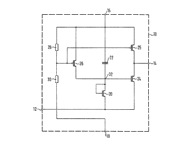
The circuit arrangement lO illustrated in Figure l comprises
an HF input 12 to which in operation a sinusoidal oscill-
36 ation is applied. It also comprises an output 14 at which
it can furnish a control signal. A terminal 16 serves as
supply voltage terminal and an input l~ serves as ground
: , - . ~ . ~ : ,
~ i
: ~. .
: ~ .,. ~. ~ ,
: :
2 ~
1,
1 terminal.
The HF input 12 is connected vlaafield-effect transistor
20 connected as diode to one plate of a capacitor 22 which
acts as storage member as will be explained hereinafter.
The other plate of said capacitor 22 is connected to the
supply voltage terminal 16. In addition, the HF input 12
is in connection with two series-connected source-drain
paths of two further field-effect transistors 24, 25
l~ading to the supply voltage terminal 16. The
connection between the two source-drain paths of the field-
effect transistors 24, 25 forms the output 14. The field-
effect transistor 20 connected as diode is connected to
the gate electrode of the field-effect transistor 24 and to
the drain electrode of a further field-effect transistor 26,
- the source electrode of which is connected to the supply
voltage terminal 16 whilst the gate electrode thereof is
connected to the gate electrode of the field-effect trans-
istor 25. Also connected to the gate electrode of the
field-effect transistor 26 is the connection point of two
resistors 28, 30 which are connected in series between the
supply voltage terminal 16 and the ground terminal 18.
The field-effect transistors 20 and 24 contained in the
circuit arrangement of Figure 1 are N-channel ~OS field-
effect transistors and the field-effect transistors 25, 26
are P-channel MOS field-effect transistors.
Due to their connection to the voltage divider comprising
the resistors 28 and 30 the field-effect transistors 25 and
26 are applied to a fixed bias voltage and act as constant
current sources; the field-effect transistor 25 acts as
load resistance for the field-effect transistor 24.
The circuit arrangement of Figure 1 operates as follows:
,.
: ~ :.
. ,,
: :: : , :: : :, . :
~:,, . : ..
1 When a sinusoidal oscillation or sine wave is applied to the
HF input 12 the circuit point 32 follows the sinusoidal
oscillation until its minimum is reached. As soon as the
sinusoidal oscillation starts to rise again the blocking
action of the field-effect transistor 20 comes into play
so that the circuit point 32 is held at the potential of
the minimum of the sinusoidal oscillation. The capacitor
22 acts as storage member for said potential of the minimum
of the sinusoidal oscillation. Via the field-effect trans-
istor 26, which is connected in parallel with the capacitor22 and as already mentioned acts as current source, a dis-
charge of the capacitor 22 takes place, the discharge time
constant being set by means of the voltage divider comprising
the resistors 28 and 30 in such a manner that within the
period duration of the sinusoidal oscillation an appreciable
discharge of the storage member takes place, i.e. the pot-
ential at the circuit point 32 is changed in positive di-
rection.
As soon as the sinusoidal oscillation at the HF input
12 again approaches its minimum and in particular again
reaches a voltage value which is lower than the potential
at the circuit point 32 (apart from the threshold voltage
at the field-effect transistor 20 connected as diode) the
field-effect transistor 20 again becomes conductive so that
a charging current flows to the capacitor 22 and as a
result the potential at the circuit point 32 is again drawn
to the minimum of the sinusoidal oscillation. The short
current pulse which flows for recharging of the capacitor
22 results in the field-effect transistor 24 changing to I ,
the conductive state for the duration of said current pulse
and consequently at the output 14 a negative pulse appears
which is clearly related to the minimum of the sinusoidal
oscillation at the HF input 12.
A preferred use of the circuit arrangement of Figure 1 is
indicated in Fig. 2 by a schematic circuit diagram.
., ,
.
~, ~:,
.
,
,J 3 ~
1 The circuit illustrated in Fig. 2 is part of a transponder
of which however only the components necessary for the ex-
planation of the use of the circuit arrangement of Figure
1 are shown. The resonance circuit 34 contained in the
circuit of Figure 2 and comprising the capacitor 36 and
coil 38 can be stimulated to oscillate by means of an H~
carrier wave pulse emitted by a transmitting device.
Said pulse may be received by an antenna, not shown in
Fig. 2, and supplied to the resonance circuit; however, only
the coil 38 can be part of the antenna. The resistor 40
lying parallel to the resonance circuit 34 is shown as rep-
resentative of all elements damping the resonance circuit
32.
A diode 42 leads from the parallel circuit of the resistor
40, the capacitor 36 and the coil 38 to ground. Parallel
to the diode there is a switch 44 which can be closed by the
control signal from the circuit arrangement 10. In prac-
tice the switch 44 is an electronic switch which on receiv-
ing the control signal from the output 14 moves from thenonconductive state to the conductive state.
In Figure 2 a supply voltage source 46 is illustrated which
in the use outlined in a transponder may consist of a cap-
acitor which is charged by rectification of the HF carrierwave pulse by means of the diode 42. The voltage at the
capacitor 46 serves as supply voltage for the circuit arr-
angement 10 and serves simultaneously as energy source from
which the resonance circuit 34 under the control OL the
control signal from the circuit arrangement 10 on each clo-
sure of the switch 44 receives an energy pulse which main~
tains the sinusoidal oscillation in the resonance circuit
34. Of course, it is only possible to maintain the sinus-
oidal oscillations for a limited period of time which depends
on the sige of the capacitor 36 and the energy stored there-
in.
. .,. :
- : :
.
.
J J ~
1,
l The circuit arrangement 10 generates the control signal at
the output 14 always in the region of the minimum of the
sinusoidal oscillations in the resonance circuit 34 and
consequently the closing of the switch also takes place in
this region. This leads to in-phase energy supply to the
resonance circuit which is a prerequisite for maintenance
of the sinusoidal oscillations.
It is pointed out that the circuit arrangement illustrated
in Figure 1 can readily be modified so that it generates
control signals in the region of the maximum of the sinus-
oidal oscillations. To do this, it would merely be necess-
ary to use P-channel MOS transistors instead of the respect-
ive N-channel MOS field-effect transistors used and vice-
versa. The use circuit of Figure ~ could also readily be
adapted to another polarity of the control signal from the
circuit arrangement 10.
ao
:. - " I
,~
,
, - :: , ,