Note: Descriptions are shown in the official language in which they were submitted.
2 ~ J V
lELECTRC)N GUN ~iVl~I I~E~lR~L S~IADOW GRID
The invention pertains to guns for linear-beam electron tubes.
S The "shadow grid" is a perforated electrode element near the emitting
cathode which is itself non-emiteing and covers areas of the cathode
Iying behind the perforated control grid conductive members to guide
the current into paths passing through the apertures in the control grid
without striking the conductive members.
Pl~OR ART
In a grid-controlled electron gun a problem is grid
bombardment by emitted electrons. This has been reduced by
electron optically shaping the cathode surface to focus the electrons
15 between and through the grid elements.
U.S. Patent No. 3,558,967 issued January 26, 1971 to G. V.
Miram discloses a "golf ball" cathode having concave dimples to direct
electrons through holes in the grid mesh. (Prior work had used
cylindrical grooves for parallel-wire grids.) This reduced interception
20 markedly, but ~here was still emission of electrons from the ridges or
flats between grooves which reach the grid bars.
Another approach was to overlay portions of the cathode
sur~ace beneath the control-grid elements with a "shadow grid" which
was non-emitting either by virtue of temperature lower than the
25 cathode's or by making it of non-emissive material. The shadow-grid
surface was elevated above the emissive surface to provide electron-
optical focusing of 'Ibeamlets" between control-grid conductors. When
the shadow grid was a separate unit above the surface of the cathode
or lying directly on it, its differential thermal expansion provoked a
89-05
-. , ~- , . . .
', , :' :
' , .
.
.' ~ ' ' .
~d ~ 7~ ~
problem of maintaining proper focus. U.S. Patent No. 3,967,150
issued June 29, 1976 to Erling L. Lien, George V. Miram and Richard
B. Neison discloses an integral shadow grid formed of non-emissive
material as an integral part of the surface of a golf-ball cathode. In
S this embodiment, the shadow-grid and cathode dimples are formed by
mechanical machining. This is expensive and limits the fineness of the
grid mesh. The mesh size must be small in guns forming the tiny
beams needed for microwave tubes generating very short wavelength.
Another embodiment of '150 involves depositing mechanically
10 removable material through a mask to cover areas intended to be
emissive, depositing non-emissive material in the masked off areas and
removing the (powdered) material from the emissive areas. This
avoids the machining limitation, but the mesh size is still limited by the
mechanical operation.
The present invention comprises a method of producing a
bonded shadow grid of very small dimensions by atomic or optical
procedures.
~UMMARY 0~ T~E n~Er~T~O~
An object of the invention is to provide a gun with a shadow
grid very close to the cathode.
A further object is to provide a shadow grid of very fine
structure.
A further object is to provide a shadow grid that is immovable
25 with respect to the cathode.
A further object is to provide a unitized cathode and shadow
grid structure which is easily manufacturable to very close tolerances.
These objects are realized by forming the shadow grid as an
integral part of the cathode structure which is deposited on the
89-05
, . ' , .
- 2~7~
cathode and machined by bombardment to very close tolerances and
very fine structure.
BRIEF DESCRIPIION OF T~IE DRAWINGS
FIGS. 1-6 are cross-sectional sketches showing the steps in
producing the inventive grid-cathode structure.
FIG. 7 is a schematic cross-section of an electron gun
embodying the invention.
FIG. 8 is a composite perspective graph of current density in
a test vehicle embodying the invention.
DESCRIPTION OF 1~3[E PREE~ERRED
EMBODIMENTS
In electron discharge devices using extended, smooth thermionic
emission cathodes an apertured control grid is often spaced in front
of the emissive surface for applying potentials to control the emitted
current. A principal drawback is that the grid often must have a
positive bias to draw the required current. This causes the grid to
draw electrons directly to the grid wire or bar elements. The grid
then emits undesirable secondary electrons. Also, the grid is heated,
resulting in expans;on movements and in severe cases to thermionic
grid emission and even melting of the grid.
These problems are most severe in linear-beam tuhes where the
electrons are converged and focused through a small anode hole.
The local electric fields around the grid elements diffract the electron
paths causing the beam to spread ancl be intercepted on the
; downstream interaction circuits.
As described under "prior art" a partial solution was to place
a "shadow" grid very near or actually on the cathode surface with
: ::
~'~, 8~-05
~' '
- ~ '' -.
:;' : .
'
~,: ; , :
:
elements directly behind the control-grid elements. The shadow grid
is designed to be non-emissive due to either a reduced temperature
or to an emission-suppressing chemical surface. The shadow gridS by
extending above the cathode surface, also provides local electric fie]d
5 directing electrons emitted near the shadow grid away from it so they
are guided by electron optics through the control-grid apertures. --
To make the control grid spatially stable, it has proved
advantageous to bond it directly to the cathode. The invention covers
an improved way to do this.
High amplification actor and electron-optical convergence of
the entire beam require a very fine-mesh grid, so that manufacture by
machinir.g methods becomes impractical for acceptable accuracy and
cost. The grid cannot be made thinner than about .002" by
conventional fabrication techniques. This excessive thickness
15 overconverges the electron beamlets and degrades the focussing. It
also increases the electrical noise level in the tube, which is a key
performance parameter in many applications. rne invention on the
other hand provides an extremely fine-grained, accurate structure
which can be made as a single unit or even as many units
20 simultaneously.
FIGS. 1-6 illustrate the steps in the process, which is important
for the final str~cture.
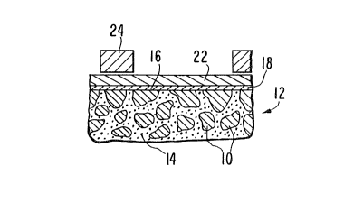
FIG. 1 is a section through a well-known impregnated cathode.
The grain sizes are e~aggerated for clarity. (:;rains 10 of tungsten or
25 molybdenum are sintered into a porous matrix 12, machined to shape
and impregnated with a molten alkaline-earth alLIminate 14. l`he
upper emissive surface 16 is smoothed by the machining.
FIG. 2 shows the result of the initial steps. For completeness,
all the preferred elements are shown, although some may be omitted
30 within the scope of the invention. A first, ve~y thin continuous layer
89-05
'~
2 ~1 2J ~
s
18 of refractory metal such as tungsten or molybdenum, is deposited
from vapor, as by sputter deposition, evaporation or by chemical vapor
deposition, on emissive surface 16. Layer 18 seals over exposed areas
20 of impregnant, preventing them from reacting with or activating the
S later-applied non-emissive shadow grid layer 22 as of zirconium. Layer
22 is deposited from vapor on top of layer 18. It has appreciable
thickness, such as S microns, to provide electrostatic focusing of
electrons near the edges of the shadow grid elements.
FIG. 3 shows the next step. An apertured mask of grid
elements 24, as of sheet molybdenum, covers the portions of layer 22
which are to become the elements of the completed shadow grid.
In FIG. 4 the deposited layers 18, 22 between mask elements
24 have been removed by bombardment, as by sputtering away in an
inert gas such as argon, or by laser etch. Emissive layer 16 is thus
~xposed between non-emissivei shadow-grid elements 26 which are
protected from removal by mask elements 24. Initial surface 16 is
thereby exposed in the emitting areas.
In FIG. S a final, activating layer 28 of a metal of the group
consisting of osmium, iridium, rhenium and ruthenium or their alloys
is vapor-deposited on the exposed surfaces. These metals are known
to increase the emission of impregnated cathodes.
FIG. 6 shows the completed cathode 12 with bonded shadow
grid 26 after removal of mask 24 so that only emitting port;ons 16 are
activated.
FIG. 7 is a schematic sketch of a grid-controlled electron gun
embodying the invention. Cathode 12 is supported via a thin meta]lic
tube 30 on the dielectric vacuum envelope (not shown, the structure
is well-known). Cathode 12 is heated by a coil radiator 32. Covering
the periphery of cathode 12, a continuous ring 34 of non-emissive
layer 22 is left to stop stray emission from the edge, and an apertured
89-05
.,
: .
- - 2~ ~2~
mesh of raised shadow-grid elements 26 is bonded to cathode 12.
Emission from active areas 28 is focussed into distinct beamlets 36
passing through apertures 38 in a metallic foil control grid 40
supported via metallic tube 42 from the dielectric envelope. The array
S of beamlets 36 forms a composite beam 44 which as a whole is
focussed by a focus electrode 46 as is well known in the art. Focus
electrode 46 is electrically connected either to cathode 12 or control
grid 40. Beam 44 is drawn to and through an aperture 48 in an
electrically isolated anode 50, whence it goes to an rf interaction
10 structure (not shown).
FIG. 8 shows the beamlet focussing in a test vehicle sirnulating
part of the inventive electron gun. A sm.all probe for current-density
measurement was scanned across the beam (right and left) at
progressive positions away from the cathode, shown in synthetic
15 perspective by vertical displacements. A Y-shaped shadow-grid
member embodying the invention was on the cathode surface, showing
the unprecedented accuracy of separation of the beamlets.
89{)5
' '' ' ' ' ' ', ; `