Note: Descriptions are shown in the official language in which they were submitted.
DAT DATA GROUP ASSEMBLY
1 BACKGROUND OF THE_INVENTION
The disclosed invention is directed generally to
computer data storage digital audio tape tDAT) systems for
digital storage, and is directed more particularly to
techniques for assembling data read from a DAT tape into
data groups with reduced buffer management.
Digital audio tape ~DAT) technology, which was
developed for audio programming, has been adapted for
storage of computer data. An example of a format for the
storage of computer data utilizing DAT technology is the
American National Standards Institute (ANSI) Digital Data
Storage (DDS~ standard, presently in draft form ("PROPOSED
AMERICAN NATIONAL STANDARD HELICAL-SCAN DIGITAL COMPUTER
TAPE CARTRIDGE 381 mm (0.150 in) FOR INFORMATION INTER-
CHANGE," ASC X3 Project No. 668-D).
The characteristics that have made DAT technology
attractive for computer data storage include high capacl-
~y, high transfer rate capability, relati~ely small media
size and low media cost, and the adaptability of DAT
technology to conform with personal computer storage
device form factors including the 5-1/4 and 3-1/2 inch
forms.
The use of DAT technology for storage of computer
data can be achieved by applica~ion of a data storage
format, such as the above-referenced A~SI DDS format, to
03089DPD 538
. ,~ .,:.. . . . ..
1 the DAT ormat. In particular, the DAT physical track
format is retained, but the contents of th~ information
stored in the tracks is in accordance with the computer
data storage format.
As is well known, reading a tape with a DAT system
requires that the digital data stream produced by reading
a computer data storage DAT tape must be organized in
accordance with a predetermined formatting convention, for
example, for transfer to a host computer. For example,
pursuant to the ANSI DDS standard, the digital data stream
must be broken into frames which are combined into groups,
where a frame comprises 2 tracks and a group includes 22
or 23 frames, depending on the level of error correction
implemented. The frames in a group must be arranged in an
ordered sequence, which may be different from the sequence
of the frames in the data stream.
In a data storage DAT tape, each frame includes a
header that identifies its relative position within its
group, and computer storage DAT systems typically utilize
such headers with buffer management for assembling frames
into groups. For example, a two step process might be
used. Each frame is transferred into a distinct frame
memory, and the next step is to move the frame to its
proper location in a group buffer which would typically be
in a separate memory. Considerations with such processing
include the use of a separate frame memory having suffi-
cient capacity to store at least two frames to allow for
processing of a frame tha~ has been completely read in
while another frame is being read into the frame memory,
and the complexity of the associated control hardware
te.g., parity generation, storage and checking).
03089DPD 538
1 SUMMARY OF THE INVENTION
It would therefoxe be an advantage to provide a
computer data storage DAT system which has reduced bufer
management complexity for assembling DAT playback data
frames into data groups.
Another advantage would be to provide a computer
data storage system DAT which does not require separate
frame memory for assembling DAT playback data frames into
data groups.
A furth~r advantage would be to provide a computer
storage DAT system which provides for the transfer of each
frame read from tape directly to its proper location in
the group buffer on the basis of subcode information.
The foregoing and other advantages are provided by
the invention in a data group assembly circuit that
includes a tape data processing circuit responsive to the
playback of DAT tape for providing for each frame a serial
frame information outpu~ including a frame header and
frame data, and an associated subcode information output,
the subcode information output being available in a~vance
of the associated frame information. A processor
responsive to the subcode information checks the validity
of the subcode information and determines the destination
group memory loca~ions of the associated frame data, such
destination group memory locations being group frame loca-
tions specified pursuant to valid subcode information or
temporary storage areas for frames havin~ invalid subcode
information. DMA circuitry transfers the frame data to
the destination group memory locations. The processor
further checks the error status of the stored frame data,
verifies the group memory locations specified by the
subcode information for frame data stored pursuant to
valid subcode information, reloca~es fra~e data stored in
temporary storage areas pursuant to frame location
03089DPD 538
:. . ~ , ~, , . : .
; , . ~ :. ~ , ' ':
, . , :
~. ~ .~i. o3 AJ~ 3
1 .information contained in the frame headers under certain
conditions, and updates a Bad Track Table to indicate the
status of the received frame data stored in the group
memory.
BRIEF DESCRIPTION OF THE DRAWING
.
The advantages and features of the disclosed inven-
tion will readily be appreciated by persons sXilled in the
art from the following detailed description when read in
conjunction with the drawing wherein:
FIG. l is a schematic diagram illustrating the
different areas on a single track of a helical scan DAT
system tape.
FIG. 2 is a generalized block diagram of a computer
data storage DAT system in accordance with the invention.
FIG. 3 is a schematic illustration depicting a group
buffer utilized in the computer data storage DAT system of
FIG. 2.
FIG. 4 is a schematic illustration depicting a frame
header storage area as utilized in the computer data
storage DAT system of FIG. 2.
FIG~ 5 is a schematic illustra~ion depicting a Bad
Track Table as utilized in the computer da~a storage DAT
system of FIG. 2.
FIG. 6 is a generalized timing diagram depicting the
timing of certain functions provided by the computer data
storage DAT system of FIG. 2.
FIG. 7 is a flow diagram of a proce~s utilized by
the computer storage DAT system of FIG. 2 for checking
subcode information.
FIG. 8 is a flow diagram of a process utilized by
the DAT system of FIG. 2 for checking the error status and
verifying the memory location of a frame stored pursuant
to valid subcode information.
03089DPD 538
.. . ,: ~
.
. ~ . . . . . . ..
~ '3~
1 FIG. 9 is a flow diagram of a process utilized by
the DAT system o FIG. 2 for checking the error status of
a frame stored in a temporary frame storage area as a
result of invalid subcode information.
DETAILED DESCRIPTION OF THE DISCLOSURE
In the following detailed description and in the
several figures of the drawing, like elements are iden-
tified with like reference numerals.
By way of illustrative example, the disclosedinvention can be implemented generally in accordance with
the AWSI DDS standard referenced in the background, and
the following is based upon conformation with ANSI DDS.
However, it should be readily appreciated by persons
s~illed in the art from a reading of the subject disclo-
sure that other recording formats can be utilized to
implement the invention.
For ease of explanation, some aspects of DDS format-
ting that are per inent to the invention will be brieflydiscussed. DDS formatting organizes da~a into data groups
respectively having 2~ or 23 frames, where each frame
comprises 2 tracks.
Referring to FIG. l, set forth therein by way of
illustrative example is a schematic layout of one track of
a computer data storage DDS DAT tape. A main area, which
; ~ corresponds to the PCM area in DAT audio tapes, stores
user data as well as data management infbrmation such a
the Logical Frame Number (LFNj of the frame with which the
particular track is associated. The LFN is the logical
position of the frame in the associa~ed data group, which
can be different from the actual physical location of the
frame due to factors such as rewri~es. Further, frames
can be out of sequence because of appends~ re writes, head
clogs during write operations, and bad tape areas. DDS
03089DPD 538
; ~ ' , ' ` ; , . " ` '
;' "kl
1 formatting supports a read-after-writs technique wherein a
frame identified as being a bad frame can be re-written
downstream of the bad frame, and no~ necessarily immedi-
ately after the bad frame. In particular, the frame can
be re-written after zero, one, two, three, four or five
other frames have been written. The subject disclosure
takes into account such read-after-write procedures~
The tape subcode areas s~ore, among other informa-
tion, the LFN of the associated frame, the Absolute Frame
Count ~AFC) for the associated frame, a subcode type
identifier, a tape area identifier, as well as other
information. The AFC represents the actual physical
location of a frame in the sequence of rames on a tape.
A data group includes 22 or 23 frames, depending on
whether a third level of error correction code (ECC) is
utilized with the group, and gxoup boundaries can be
indicated by amble frames which have an LFN of 0, or by a
frame that has an LFN of 1. However, with read-after-
write, the last frames in one group could be meshed with
the initial frames in the subsequent group, and the
procedure fox reading groups will need to recognize and
properly process this circumstance.
The ATF ~automatic track finding) areas con~ain
tracking information utilized for centering the tape heads
on the tracks on the tape.
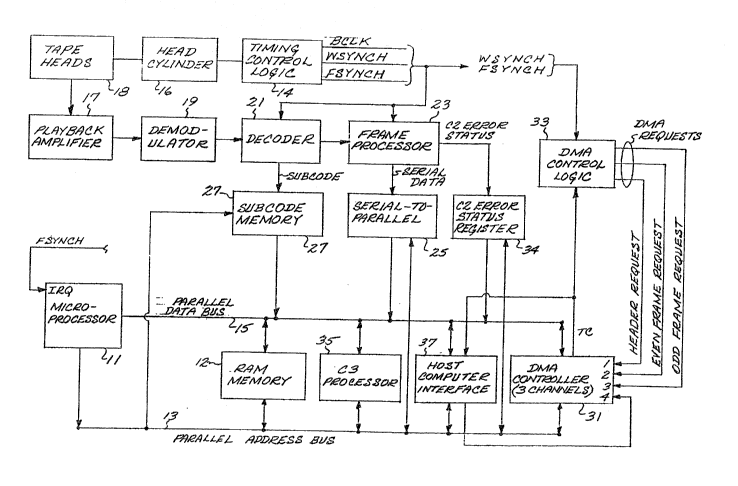
Referring now to FIG. 2, shown therein is a genex-
alized block diagr~m of read components of a computer data
storage DAT system in accordance with t~e in~ention. A
microprocessor 11 provides overall control via a parallel
address bus 13, a parallel data bus 15, and other lines as
described further herein. A random access memory 12
connected to the address bus 13 and the data bus lS is
utilized by the microprocessor 11 for data group buffering
as well as other memory functions. Other components are
coupled to the address and data buses, and it should be
03089DPD 538
.. ,: . - .".., ,:.,
. ,,, ,, , . : ; ;:
~ ,J ~ . ~
1 appreciated that address decoding circuitry would be
utilized as appropriate. For ease of illustration such
addres~ decoders are not depicted in the block diagram of
FIGo 1~
S The DAT system further includes a timing logic
control circuit 14 which is synchronized with the rotation
of a rotating head cylinder 16 that supports read and
record tape heads 18. The timing logic control 14 pro-
vides timing signals pertinent to processing and organiz-
ing the data read by the DAT system. In particular, the
timing signal generator provides a frame sychronization
signal FSYNCH which defines frame boundaries, a word
synchronization signal WSYNCH which defines word bound-
aries, and a bit clock BCLK.
A tape playback amplifier 17 responsive to the read
heads provides its RF playback signal to a demodulator 19
which provides an output comprising a serial bit stream
that includes information from the subcode areas and the
main areas of ~he tape. The output of the demodulator 19
is processed by a decoder 21 which provides, for example,
a first level of error correction code ~ECC) processing on
the demodulated signal, for example the Cl ECC pursuant to
the ANSI DDS standard, as well as decomposition of the
demodulated data into frame information and subcode
information.
~he frame information output of the processor 21 is
provided to a frame processor 23 which applies a second
level of ECC processing, for example C2'ECC pursuant to
the DDS format, and de-interleaves the frame information
from the two tracks comprising a frame to provide a serial
frame output. The serial frame outp~t for each frame
includes a frame header ~e.g., 2 words wherein each word
comprises 2 bytes) and frame data (e.g., 2878 data words~
which are provided to a serial-to-parallel conversion
circuit 25 for transfer to the RAM 12 by direct memory
03089DPD 538
~ ~ .
" ."" ~';
C~ J ~i ~
1 access (DMA) processing. The serial-to-parallel conver-
sion circuit 25 is clocked by the timing signali provided
by the timing logic control 14, and transforms the serial
frame output into parallel frame da~a words.
The frame processor 27 further provides error status
outputs, for example to a C2 error status register 34. In
particular, the error status output~ will indicate which
track includes an error, if any, that could not be cor-
rected by C2 ECC.
The subcode information for each frame is stored by
the decoder 21 in a subcode memory 27, which, for example,
can be a random access memory dedicated to the decoder 21.
The subcode memory ~7 also stores Cl error status indica-
tive of whether Cl processing detected any block errors
that could not be corrected by Cl processing.
A four-channel DMA controller 31 i5 connected to the
address bus 13 and the headers and data bus 15 for DMA
transfer of fr~me data from the serial-to-parallel shift
register circuit 25 to the RAM 12. A DMA control logic
circuit 33 responsive to timing signals provided by the
timing logic control 14 and the terminal count (TC) signal
from the DMA controller 31 provides the DMA requests to
the DMA controller 31.
An error correction code (ECC) processor 35, for
example for providing C3 ECC processing in accordance with
the ANSI DDS standardt is coupled to the parallel address
bus 13 and the parallel data bus 15, and provides for ECC
processing o~ data groups assembled in th~ RAM 12.
A ho~t computer interface 37, for example in accor-
dance with the ANSI Small Computer System Interface (SCSI)
~tandards~ is also coupled to the parallel address bus 13
and the parallel data bus 15 for transferring the data
retrieved from the DAT tape to a hos~ computer. Puriuan~
to known configurations, the host computer interface
utilizes DMA techniques and provides DM~ requests to
03089DPD 538
~!'.' . . . ' . '
' ' , . ' `. ' i ' '. ':1 ' ~ ' '" "; ''
' " . ' ',, " ' ;~' '. . ' .,
1 channel 4 of the DMA controller 31. The host computer
interface 37 also receives the TC signal from the DMA
controller 31.
The foregoing components of the DAT read system can
be partitioned as required for the particular application.
For example, for use with personal computers such as the
IBM AT which have DMA controllers, the microprocessor 11,
the ~M 12, the address bus 13, the data bus 15, and the
DMA controller 31 could comprise components of the per-
sonal computer. The serial-to-parallel conversion circuit
25, the DMA control logic 33, and the ECC processor 35
would be on a plug-in peripheral interface card, and the
host computer interface 37 would not be needed. The
demodulator, the decoder, the subcode memory, and the
frame processor would be included, for example, with the
drive mechanism.
By way of further alternative, for use with a host
computer interface, for example, in accordance with the
ANSI SCSI standards, the microprocessor 11, the RAM 12,
the address bus 13, and other related components woula be
part of a dedicated controller. The dedicated controller
could be housed with the drive mechanism, for example.
Referring now to FIG. 3, schematically shown therein
is the logical organization of a data group buffer 100 in
the RAM 12 for storing frame data ~without frama headers)
for a 23 frame group, for the illustrative example wherein
an ECC frame is included in accordance with the ANSI DDS
standard. The group buffer 100 also in~cludes temporary
frame storage locations A and B which are utilized in the
event of bad tracks, invalid subcodes, or C2 ECC errors,
as described more fully herein. Each frame area is 5,756
bytes of memory, and is identified by frame number. By
way of illustrative example, three (3) to seven (7~ data
group buffers can be utilized, depending upon the
processing requirements and implementation.
03089DPD 538
.: . -
,~ .. .
,, , ~ :' .,,; . -' ' , : . .
.. : . . . ' , ~:'
~ a~
1 Referring now to FIG. 4, shown therein is a four
byte header storage area in the RA~ 12 which is utilized
for storage of the headers of the frames in a data group.
Depending upon implementation, only a few header storage
areas are utilized as required.
Referring now to FIG. 5, shown therein is the
logical organization of a Bad Track Table (BTT) in the RAM
12 which is utilized for storing track status codes
indicative of the status of each of the 46 tracks of a
data group being processed. The entry for each track
comprises 4 bits, for example, which can be coded to
include the following~
0 = not received
1 = received, no error
2 = received, error
3 = good track replaced by bad track
A Bad Track Table is utilized to determine whether re-read
of a group is necessary, and for further functions as
described herein. Prior to use for a particular group,
the entries of a Bad Track Table are initialized to
indicate that that no tracks have been received. A
plurality of Bad Track Tables are utilized as appropriate.
Referring now to FIG. 6, shown therein is a timing
diagram showing, relative to the frame synchronization
signal FSYNC~, the contents of the subcode memory 21, the
serial frame output of the frame process~r 15, the status
of the terminal count signal TC, the frame data being
transferred by DMA, the DMA channel setup, and the error
checking functions provided by the microprocessor 11.
During the particular cycle "A" of the synchro-
nization signal FSYNCH, the subcode informa~ion for the
frame N is available and is accessed by the microprocessor
for processing, as discussed in further detail herein, and
03089DPD 538
; . . ~ : . .. . . ;;: . ~ . : . . .
-. : . ........... . . . , .. , , , ~, :: , ... :: .
,: : .. ...
'~ ~ ,. , ' ' , .' ' . ! .
~ ëi~3
11
1 the frame header and data for the preceding frame N-l is
being transferred by DMA from the serial-to-parallel
conversion circuit 25 to the RAM 12, starting with the
frame header. Further during the cycle "A," the DMA
channel 1 is active until the frame header for the frame
N-l has been transferred to a frame header area in the RAM
(as indicated by the Terminal Count signal TC from the DMA
controller 31~, and then the DMA channel 3 becomes active
(based on N being even) for transfer of the frame data to
the group buffer area. While the DMA channel 3 is active,
the DMA channels 1 and 2 will be set up with address and
transfer count information by the microprocessor 11.
Further during the FSYNCH cycle "A," the microprocessor 11
checks the results of the C2 ECC processing to determine
whether there is a bad track in the frame N-2, which has
already been stored in a group buffer in the RAM 12, and
also checks the LFNs of the header for the frame N-2 as
detailed further herein.
During a given cycle of the synchronization signal
FSYNCH, the subcode check, the C2 and header check, and
the DMA set up are performed by the microprocessor pursu-
ant to an interrupt generated by the synchronization
signal FSYNCH, while the DMA transfer is performed by the
DMA controller. The functions provided by the micropro-
cessor are performed sequentially, and the timing diagramof FIG. 6 is intended only to indicate tha~ a given cycle
of the synchronization signal FSYNCH defines a time window
during which such functions are to be performed.
From the foregoing, it should be appreciated that
during a given FSYNCH cycle, three successive frames are
in different processing stages and are being processed in
a pipeline manner, with the DMA channels 2 and 3
alternating from one cycle to another so as to maintain
the continuous transfer of frame data to group buffers in
the RAM 12. It should also be appreciated that the
03089DPD 538
~ ,. : ... i ,, ,; . . . .
, , f: . :., -:
.: .. , .~ ::
:. . : ~ . . : ~:
12
1 processing of each frame requires three (3) cycles of the
frame synchronization signal FSYNCH, with predetermined
procedures taking place during each cycle.
By way of illustrative example, DMA transfers are
controlled such that the terminal count signal TC is
indirectly slaved to the synchronization signal FSYNCH,
and the signal TC is utilized by the DMA control logic to
make the appropriate DMA requests. Pursuant to such DMA
control, hiowever, it should be appreciated that initiali-
zation will be based on the frame synchronization signal
FSYNC~i, and will involve "dummy" DMA transfers as
controlled by the microprocessor 11 until the target group
is reached.
The procedure for reading and storing data groups is
generally as follows for a given frame. As discussed
above, a frame is processed over three successive cycles
of the frame synchronization signal FSYNCH, with different
procedures occurring during a given cycle. As the play-
back of each frame is received by the processor 21, the
subcode information is transferred to the subcode memory
while the frame data continues to be processed, which
allows the subcode information to be checked and examined
before the corresponding frame data becomes available at
the output of the frame processor 27. In par~iicular, the
subcode data is examined during the first FSYNCH cycle
pertinent to a given framie to determine whetiher at least
one block of the repeated subcode data in the two tracks
comprising the frame meets ~ihe following ariteria:
- Cl ECC processing check indicates no error
- parity check indicates no error
- subcode type identifier indicates data area
- AFC is greater than the previous good subcode AFC.
These check~ are provided to reduce the probability
of an undetected subcode error.
03089DPD 538
- . . i ~ ; . . I ~ .
13
1 If the available subcode information from each track
meets the foregoing criteria, but the verified subcode
information from one track differs from that of the other
track, then subcode data for the current frame is con~
sidered invalid (because both tracks must be from the same
frame and subcode information from the 2 tracks should be
identical).
If there is no subcode error, the Logical Frame
Number (LFN) contained in the subcode information is used
as an index into the group buffer utilized for the partic-
ular group beinq processed. The DMA transfer takes place
during the second FSYNCH cycle pertinent to the given
frame. The DMA channel currently idle (odd or even) and
the header DMA channel are set to direct the next incoming
frame to the address which has been calculated by the
microprocessor.
After a frame has been read into a group buffer,
during the third FSYNCH cycle pertinent to the given
frame, a check is made to determine if there were any C2
detected errors. Also during the third FSYNCH cycle for
the given frame, ~he frame header Iwhich includes the LFN
information from each of the tracks comprising the frame),
is examined to determine whether the header LFN's match
the subcode LFNs which were previously determined to be
identical. If the header LFNs are the same as the subcode
LFNs, and there is no C2 error, then the Bad Track Table
entry for that frame is upd~ted to indicate that a good
frame has been received. (The BTT was first initialized
to indicate that no tracks were received).
If the C2 error check indicates an error, the BTT
entries are checked to see if the just read frame in error
has overwritten a frame which was previously correctly
read into the same storage area. If a prior good frame
was just replaced with a bad frame, the AFC of the frame
just written to the group buffer i5 saved and the BTT i~
03089DPD 538
:
i, : , ,
14
1 updated. This may be used to recover a good copy of the
frame during a subsequent "modified" re-read attempt,
described below, wherein a frame matching a saved AFC is
processed as having an invalid subcode so that it will not
be used to over-write a good frame.
If the subcode information is invalid, then the LFN
cannot be reliably determined until after the frame has
been read to memory. So the frame is directed to one of
the two Temporary Frame Storage areas in the group buffer.
Either area may be used, so long as it is not otherwise in
use. (In the case of two successive frames with subcode
errors, both areas will be needed.)
After the frame data has been xead to the Temporary
Frame Storage area, the C2 error status is checked. The
header is also checked to determine that both tracks
comprising the frame have the same LFN. If the header
LFNs agree, and there is no C2 error, the frame is moved
to its correct storage area in the group buffer (as
determined by the header LF~). The move is done at a
relatively high speed so that it is complete before the
next frame has been stored. tDuring the move, another
frame may be incoming to any one of the other frame
storage areas.) For example, the microprocessor 1l may
execute a MOVE STRING instruction to perform a memory-to-
memory move at high speed. Also, the Bad Track Tableentry for the frame that was moved is updated to indicate
receipt of a good frame. In this manner, groups may be
assembled without the of subcode information.
If a single track is in error in a frame determined
- 30 to have invalid subcode information, then the Bad Track
Table entry for the LFN identified by the good track is
checked. If no prior track is present, the just-received
frame is moved to its location in the group buffer being
utilized for this group and the BTT i5 updated. Other-
wise, i the track LFNs differ, or a C2 ECC error is
03089DPD 538
.~ . ^ . ' . ' ' ' ' `
.^' .' '" ' '. ~ ~
~,
~ $ ~il
1 detected, the present frame is ignored, and the TemporaryFrame Storage area may be re-uæed for a subsequent frame.
By way of particular example, in accordance with the
re-write rules of the DDS format, assembling of the frames
for the current group is completed when any of these
conditions is de~ected using valid subcode information:
- A frame from the next group in sequence has
been read, and its LFN is > or = 6.
- The current frame's AFC is > or = the AFC +6 of
the last correctly received final frame (last
frame) in the current groupO
- Six amble frames have been received.
- An End of Data (EOD~ marker is detected.
Handling of re-write sequences which contain frames
from two groups, and other details of traversing group
boundaries (such as handling multiple group buffers) are
done in a straightforward manner. Subcode information can
used to perform those functions, if available.
If a frame with a LFN of 12 or greater has been
correctly received, then further frames with LFNs of one
to six will not be accepted into the current group~ This
eliminates the possibility of the first frames from the
following group being accepted as frames from the current
group (due to the rewrite capability with the ANSI DDS
standard, detection of a possible rewrite sequence re-
quires reading at least six frames beyond the end of the
current group~.
The rejected frames will be treated as frames from
the next group. They may be directed to an appropriate
group data buffer area for processing, or discarded,
depending on implementation.
After a group has been read (as determined by the
3S above criteria), a check is made to determine if another
03089DPD 538
,: , , .. . " ~ ;
: , ,
....
., .~ : .
16
l read pa59 iS necessary. If a third level of error check-
ing is used, for example, C3 ECC in the DDS format, one of
two bad tracks may be corrected, and so a re-read is
unnecessary. If no C3 ECC is used, then all frames must
be read correctly. The Bad Track Table is examined for
the presence of bad tracks, and a decision to re-read or
not re-read, according to the appropriate criteria.
When a re-read pass is made, the previously read
good frames are saved, so that only the erroneous frames
need to be recovered. Thus, not all frames must be read
correctly in any single read pass. However, the incoming
subcode and frame data are processed in the same manner as
in the original read pass.
If successive re-reads fail to recover all the
necessary frames, a "modified re-read" may be performed~
This is used to ignore the defective final copy of a
repeated frame, in the case of an earlier copy had been
correctly received. This is expected to happen rarely,
since the last copy of a rewritten frame should be ver-
ified as good by a read-after-write check.
In a modified re-read, any frames which contain a
valid subcode AFC value ma~ching one of the previously
saved AFCs is treated as if it has an invalid subcode.
This prevents the defective frame identified by the saved
AFC from overwriting a previous good copy.
In the normal case without subcode or frame data er-
rors, all frames in each group are directed to their
correct storage areas, without being moved from the
Temporary Storage area and without re-read passes.
In the infrequent case of not all frames being read
in the first pass, successive re-read passes can be made
to accum~late good frames during multiple group reads.
In the worst case of no valid subcode on any frame,
every ~rame will be read into the Temporary Frame Storage
area, then moved to its correct storage area if the frame
03089DPD 538
.: . , :: , . :,
:. : :. :
".; '''' : ''.',', :.
17
1 data is good. Thus, this procedure properly stores fxame
data in the group buffer even if no subcode information is
present.
Spurious frames between groups and incorrectly
recorded frames are eliminated by allowing a later copy of
a frame to replace an early copy. If the later, original-
ly correctly recoxded copy becomes unreadable, a previous
copy can be used during a later re-read attempt using
"modified" re-reads as previously described. This also
corrects the unlikely event that subcode data had an
undetected error.
An extensive section of bad or damaged tape (with
little or no valid subcode and little or no good frame
data) can be correctly handled because the reading pass
continues until the detection of good frames in a subse-
quent recorded area.
Referring now to FIG. 7, shown th~rein is a process
in accordance with the invention for checking subcode
information, which is executed pursuant to an interrupt
generated by FSYNCH
At 111 the Logical Frame Number (LFN) of the frame
whose subcode information is available is read from the
subcode memory 27. At 113 a determination is made as to
whether the subcode information contains an error, check-
ing for example that the Cl ECC processing by the proces-
sor 21 did not indicate an error, that parity check
indicates no error, that the subcode type identifier
indicates data area, and ~hat the Abco~ute Fram~ Count
(AFC) is greater than the previous valid subcode AFCo If
the subcode information oontains an error, then at 114 the
DMA controller 31 is set up to direct the frame data
associated with th~ subcode information just processed to
one of the temporary frame s~orage areas. The process is
then exited.
03089DPD 538
,
' , . ' '
18
l If the determination at 113 is no, the subcode data
does not contain an error, a determination is made at 115
as to whether the LFN's of the subcode information for
bo~h tracks of a frame are the same. If no, control
transfers to 114, discussed above, for setting up the DMA
controller to direct the frame data to one of the
temporary storage areas.
If the determination at 115 is yes, the subcode
LFN's for the two tracks of a frame are the same, a
determination is made at 117 as to whether it was
previously determined that processing had extended into
the next group (discussed below) and the subcode LFN is
greater than or equal to six. If yes, reading of the
present data group is complete and the process is exited.
If the determination at 117 is no, a determination is made
at 119 as whether the subcode AFC is greater than or equal
to 6 plus the AFC of the valid final frame in the data
group. ~A valid final frame in a group is a correctly
received frame 22 or 23, depending on implementation). If
yes, reading of the present data group is complete. If
the determination at 119 is no, a determination is made at
121 as to whethex 5 successive ambles have been received.
If yes, reading of the present data group is complete. If
the determination at 121 is no, 6 successive ambles have
not been received, a determination is made at 123 as to
whether the subcode LFN is less than or equal to 6. If
no, processing continues at 127.
If the determination at 123 is yes,'the subcode LFN
is less that or equal to 6, a determination is made at 125
as to whether a frame having an LFN greater than or equal
to 12 has already been correctly rec ived for the present
group. If yes, the present frame is regarded as being for
the next group and is buffered or discarded as appropri~
ate, and the process is exited. If the de~ermination at
3~ 125 is no, processing continues at 127.
03089DPD 538
: , . . . : , -
:.: :, . : . .
~: : , : :, :
~: ;
19
1 At 127 a determination is made as to whether the
present subcode information is from a modified re--read,
discussed above. If no, processing continues with 131.
If the determination at 127 is yes, the present data is
from a modified re-read, a determination is made at 129 as
to whether the current AFC ..:atches the AFC of a bad frame
saved from a prior read. If no, procassing continues at
131. If the determination at 129 is yes, the present AFC
matches the AFC of a previously saved bad frame, control
transfers to 114 for set up of the DMA controller to
transfer the frame information to one of the temporary
frame storage areas. This prevents overwriting of a good
frame in the group buffer since the AFC had been previous-
ly saved to indicate that a good frame had been overwrit-
ten with the bad frame having the saved AFC.
At 131 the microprocessor 11 instructs the DMAcontroller to direc~ the frame d~ta to the locations in
the group ~uffer starting at the address defined by the
subcode LFN. The subcode check process is the exited.
Referring now to FIG. 8, shown therein is a process
for checking the C2 error status and the header fcr a
frame that was DMA transferred pursuant to a determination
in FIG~ 7 that the associated subcode information was
validO This process is also executed pursuant to an
interrupt generated by the synchronization signal FSYNCH,
for example after ~he subcode check process of FIG. 7.
Howe~er, it should be appraciated that for th~ same cycle
of the synchronization signal FSYNCH, the stored frame
processed by the C2 and header check process of FIG. 8
will be for the fr~me that is two (2) frames behind the
frame whose subcode information was processed with the
subcode check process of FI~. 7 (e . g ., C2 and header check
for stored frame N-2, and subcode check for frame N in the
same FSYNCH cycle).
03089DPD 538
', , :
.
G-~ ~ r ~
1 At 135, a determination is made as to whether the C2
ECC proce`ssing by the frame proceRsor 23 indicated an
error in one of the tracks of the frame. If yes, process-
ing goes to 141. If no track error was found at 135, a
determination is made at 137 as to whether subcode LFN and
the frame header LFN match. If yes, then at 139 the Bad
Track Table entries for this frame are updated to indicate
that both tracks are good. If the determination at 137 is
that the subcode and header LFN's do not match, processing
continues at 141.
At 141 a determination is made as whether the Bad
Track Table entries for thi~ frame indicat~s that this
frame is good (e.g., pursuant to a prior read and the
present read is a xe-read3. If no, the Bad Track Table is
updated at 142 to appropria~ely indicate that one or zero
good tracks were received, as indicated by the C2 error
status. The C2 and header check process is then exited.
If the determination at 141 is yes, the Bad Track
Table indicates that ~his frame was a good frame, at 143
the Bad Track Table entries for the present frame are
updated to indicate that a good frame has been replaced by
a bad frame. At 145 the AFC (absolute frame count) of the
present frame is saved for use during a modified re-read
process. The C2 and header check process for frames
stored pursuant to valid subcodes is then exited.
Referring now to FIG. 9, shown therein is a process
for checking the C2 error status and the header for a
frame that was DMA transferred to a 'temporary frame
stor~ge area pursuant to a determination in FIG. 7 tha~
the associated subcode information was not valid. This
process is also executed pursuant to an interrupt generat-
ed by the synchronization signal FSYNCH, for example after
the subcode check process of FIG. 7. ~owever, i~ should
be appreciated that for the same cycle of the synchro-
nization signal FSYNCH, the stored frame processed by the
03089DPD 538
: ., . -;
. ~ , , , . .
- .
,. ~ ; , , ~:
~ ~i . 3 ~~
21
1 C2 and header check process of FIG. 9 will be for the
frame that is two (2) frames behind the frame whose
subcode information was pxocessed with the subcode check
process of FIG. 7 (e.g., C2 and header check for stored
s frame N-2, and subcode check for frame N in the same
FSYNCH cycle). Moreover, the process of FIG. 9 is execut-
ed only as to stored frames that were found to have
invalid subcode information.
At 215 a determination is made as to whether the C2
ECC processing by the frame processor 23 for the present
frame detected an error. If yes, an error was detected, a
determination is made at 219 as to whether the C2 error
was a single track error. If no, the process is exited,
and the frame stored in the temporary storage area is
effectively discarded. If the determination at 219 is
yes, the C2 error was a single track error ~i.e., only one
track was bad), at 221 the Bad Track Table entries as
indicated by the LFN from the good track are checked. At
223 a determination is made as ~o whether such Bad Track
Table entries indicate that a good frame is already
present in the group buffer. If yes, the process i5
exited to avoid over-writing a good frame with a bad
frame. If the determination at 223 is no, control trans-
fers to 225.
If the determination at 215 is no, there i no C2
error, a determination is made at 217 to determine if the
LFN's in the frame header for the two tracks comprising
the frame are the same. If yes, process~ng continues at
225. If the determination a~ 217 is no, the LFN's from
both tracks are not the same, the process is exited and
the frame stored in the temporary storage area is effec-
tively discarded.
At 225 the present frame is moved from the temporary
storage area to the group buffer at the address as in-
dicated by the LFN for the frame, which can be the LFN
03089DPD 538
. . , ~ . . .
.
- ,. .- ' ~ -
.
:. : .. ,
~ . ., . . :
22
1 from the good track where a ingle track erxor was found.
At 227 the`Bad Track Table is updated to show a good frame
or a good track for the frame, depending on whether a
single track error was found. The process is the exited.
To summarize the foregoing processes, during each
cycle of the synchronization signal FSYNCH, the following
take place:
(a) The subcode information for frame N is being
checked pursuant to the subcode check process
of FIG. 6.
(b) The frame information for the fram~ N-l is
being transferred by DM~ to an area of a group
buffer area in the random access memory.
(c) The C2 error status and the frame header
information for the frame N-2 stored in the
random access memory are checked pursuant to
one of the processes of FIG. 8 or FIG. 9. If
the frame N-2 is stored in a temporary frame
storage area and transfer to memory is deter-
mined to be appropriate~ it would be trans-
ferred.
As to implementation, it has been discussed previ-
ously that the processes of FIGS. 7, 8, 9 are executed by
2s the microprocessor 11 pursuant to an interrupt generated
by the synchroniæation signal FSYNCH, while the DMA
transfers are controlled by the Terminal Count signal TC
provided by the DMA controller. For exam~le, pursuant to
an interrupt generated by FSYNCH, the process of FIGo 7 is
executed, which would be followed by the process of FIG. 8
or FIG7 9, as appropriate.
~h~ foregoing has been a disclosure of a computer
data storage DAT sys~em which has reduced memory and
memory management complexity, advantageously utilizes
subcode logical position identifiers, and also func~ions
03089DPD 538
~ . : . , . . . . , .:
~: :
- . , , ., ,;~
,
. . :
23
1 without such subcode logical position identifiers.
Further, the disclosed data storage DAT system provides
greater reliability since subcode information is more
reliable than frame data~ For example, a defect or
scratch on the tape can cause an error which cannot be
corrected by the frame data ECC, or a tracking problem may
be such that the frama data cannot be read reliably, but
the subcode information can be read reliably. In general,
data reliability is increased since frame data can be
assembled using either subcode information or frame data
headers for control. Data can be retrieved if either the
subcode information is bad or the frame data is bad. The
foregoing further advantageously provides for pipeline
processing of the received frames which allows for contin-
uous and efficient procassing of the tape data beingplayed back.
Although the foregoing has been a description and
illustration of specific embodiments of the invention,
various modifications and changes thereto can be made by
persons skilled in the art without depaxting from the
scope and spirit of the invention as defined by the
following claLms.
03089DPD 538
. .
. ~ . :
.
.;" ' ` ' ` ' .:
. , , :