Note: Descriptions are shown in the official language in which they were submitted.
2(~13296
MEMORY DRIVE DEVICE AND METHOD
BACKGROUND OF THE INVENTION
This invention relates to a semiconductor memory
device and method such as a RAM or an EPROM assembled in
apparatus such as a telephone system, etc., and more
particularly to a memory drive device and method
including a control circuit for controlling an access to
the memory, and having a function of resetting the state
of the control circuit at the time when a power supply of
the equipment is turned on, or at the time of recovery of
interruption to service, etc. and a memory drive method
using this device.
Generally, semiconductor memories become operative
by delivering an address signal and various control
signals from a memory control circuit such as a
microcomputer to such memories. In apparatus, such as,
for example, a telephone system including a semiconductor
memory incorporated therein, at the time of turning a
power on, or at the time of recovery of service
interruption, it is necessary to deliver, to a memory
control circuit, a reset command in order to initiate the
operation in a normal state to return its internal status
to a predetermined initial state.
In the case where semiconductor memories are of the
type necessary to be supplied with a power at all times,
such as a RAM or an EPROM, a backup power supply is
required for ensuring supply of power at the time of
service interruption of a main power supply. Since such
a backup power supply is ordinarily a battery, it is
dissipated when used for a long time. In the case where
the main power supply service interruption is recovered
after the backup power supply has been dissipated,
information stored in a memory have been already
deteriorated or vanished. Accordingly, it is necessary
for initiating a normal operation to clear the
information stored in the memory. This clear operation
2 2~132~6
is praetically carried out by delivering a memory clear
command when a reset eommand is delivered to the memory
control circuit.
As described in detail later, conventional memory
drive devices include a RC time eonstant cireuit
eonneeted to the main power supply line as a eireuit for
delivering a reset eommand to the memory control eireuit.
This RC time eonstant eircuit generates a voltage signal
gently rising in a ramp form depending upon a time
eonstant when a main power supply voltage has rised in a
step form at the time of turning a main power supply on,
or at the time of reeovery of interruption to service.
This voltage signal is applied to the memory control
circuit as a reset signal. When the memory control
circuit has been operative by the step-shaped rising of
the power supply voltage, the reset signal is in the
state where its voltage level is lower than a
predetermined threshold level, i.e., its logic level is
low ("L"). The memory eontrol eireuit reeognizes the "L"
level of the reset signal as a reset eommand, thus to
initialize the internal status.
However, in the ease where the main power supply
voltage gently rises in a time nearly to a time eonstant
of the RC time eonstant eireuit or more for any reason,
since the reset signal is in the state where the voltage
level is higher than a threshold level, i.e., the logic
level is high ("H") when the memory control circuit has
been in an operating state, there is the problem that the
memory control circuit cannot be reset.
Further, such conventional memory drive circuits
only include a manual switch for the purpose of
delivering a memory elear eommand to the memory eontrol
cireuit. Namely, whether memory should be eleared or not
depends upon the judgment by user. However, there is
great possibility that user forgets clearing the memory
without being aware of dissipation of the backup power
supply.
3 2l~i3296
As stated above, the conventional memory drive
devices cannot ensure that the operation of the apparatus
is initiated in a normal state at the time when a main
power supply is turned on, or at the time of recovery of
interruption to service.
SUMMARY OF THE INVENTION
An object of this invention is to provide a memory
drive device which is constructed to securely reset the
memory control circuit at the time when a main power
supply is turned on, or at the time of recovery of
interruption to service, thereby making it possible to
normally initiate the operation of the apparatus.
In accordance with this invention, there is provided
a memory drive device comprising a semiconductor memory,
a memory control circuit for controlling the operation of
the memory, the control circuit including a reset
terminal and operative to initialize the internal status
when a reset signal of a predetermined level is applied
to the reset terminal, and a main power supply for
delivering a power to the memory and to the memory
control circuit, the memory drive device comprising: a
comparator means which compares an output voltage from
the main power supply with a predetermined threshold
voltage, and detects rise of the supply voltage to a
predetermined voltage level, and delivers detection
signals, and a rest means which applies to reset signals
to reset terminals of the memory control circuits at
least for a predetermined period of time in response to
the detection signals delivered from the comparator
means.
In the device according to this invention, if an
output level of the main power supply rises up to a
predetermined threshold voltage at the time when a main
power supply is turned on, or at the time of recovery of
interruption to service, a reset command is then
generated for a predetermined time period. When that
time period is set to a sufficient length, reset
2Q1 3~6
4 20375-655
operation of the memory control circuit is securely carried out
irrespective of a rise speed of the main power supply.
In a preferred embodiment of this invention, there is
further provided means for generating a third signal which takes
different logic levels depending upon whether or not the backup
power supply is dissipated. This third signal is delivered to the
memory control circuit as a memory clear signal. Where the backup
power supply has been already dissipated before the main power
supply is turned on, or before interruption to service is
recovered, the memory control circuit securely receives a memory
clear command to clear the memory after the main power supply is
turned on, or after service interruption is recovered.
According to another broad aspect of the invention there
is provided a memory drive device comprising a semiconductor
memory, a memory control circuit for controlling the operation of
the memory, the control circuit including a reset terminal and
operative to initialize the internal status when a reset signal of
a predetermined level is applied to the reset terminal, and a main
power supply for delivering a power to the memory and to the
0 memory control circuit,
the memory drive device comprising:
first reset means operative to receive an output voltage of
said main power supply to generate a signal changing from a first
logic level to a second logic level at a speed dependent upon a
predetermined time constant at the time of rise of the output
voltage, thus to apply it to the reset terminal,
comparator means for comparing the output voltage of the main
power supply with a predetermined threshold voltage, and
B
- 20 1 3296
4a 20375-655
second reset means responsive to an output signal from the
comparator means to forcedly maintain an output signal from the
first reset means at the first level for a predetermined time
period.
According to another broad aspect of the invention there
is provided a memory drive method using a memory control circuit
for controlling the operation of the memory, the control circuit
including a reset terminal and operative to initialize the
internal status when a reset signal of a predetermined level is
applied to the reset terminal,
the memory drive method comprising the steps of:
comparing a feed voltage to the main memory and the memory
control circuit with a predetermined threshold voltage and for
outputting a detection signal after detecting that the feed
voltage reaches a predetermined voltage, and
in response to the detection signal, applying the reset
signal for at least a predetermined period of time to the reset
terminal of the memory control circuit.
BRIEF DESCRIPTION OF THE DRAWINGS
In the accompanying drawing:
Figure 1 is a block diagram showing an entire circuit
configuration of a conventional memory drive device;
Figure 2 is a block diagram showing an entire circuit
configuration of a memory drive device in accordance with an
embodiment of this invention;
Figures 3A to 3D are signal waveform diagrams showing
the operation at the time of recovery of power interruption of the
memory drive device in accordance with the embodiment of this
B
`` 2013296
4b 20375-655
invention;
Figure 4 is a circuit diagram showing another embodiment
of the reset signal output circuit; and
Figure 5 is a circuit diagram showing further another
embodiment of the reset output circuit.
DESCRIPTION OF THE PREFERRED EHBODIHENT
Figure 1 is a block diagram showing the circuit
arrangement of a conventional memory drive device.
In Figure 1, the stabilized power supply circuit 1
serves as a main power supply of this device. This power supply
circuit 1 receives an AC voltage of 100 V from a commercial power
supply to generate a DC constant
Z~i3296
voltage. This DC voltage is delivered through a main
power supply line 10a to a power supply voltage sense
circuit 7, a RC time constant circuit 15, and a memory
control circuit (e.g., a microcomputer) 4, and is also
delivered through the main power supply line 10a and a
reverse-current prevention diode 13 to a memory 3. The
memory backup power supply 9 may be, e.g., a battery for
effecting a memory backup at the time of service
interruption. When connected to the power supply line
10b as a result of the fact that a relay switch 8 is
turned on, the memory backup power supply 9 delivers a
backup power to the memory 3 through the power supply
line 10b and the reverse-current prevention diode 14.
The power supply vo~tage sense circuit 7 senses that
an output voltage from the stabilized power supply
circuit 1 is lowered below a predetermined value due to
service interruption, etc. of the commercial power supply
to turn the relay switch 8 on to initiate the backup
operation. The memory 3 is comprised of a semiconductor
memory of the type required to be supplied with a power
at all times, such as, for example, a RAM or an EPROM.
Ordinarily, the memory 3 receives a power from the
stabilized power supply circuit 1 to operate in
accordance with an address signal or control signals from
the memory control circuit 4. In contrast, when an
output voltage from the stabilized power supply circuit 1
is lowered by an extraordinary state of the commercial
power supply such as a service interruption, the memory 3
receives a power from the memory backup power supply 9 to
retain data stored therein.
The RC time constant circuit 15 delivers a reset
signal of which logic level is low ("L") only for a time
period determined depending upon the time constant of the
resistor 5 and the capacitor 6 to the reset terminal RS
of the memory control circuit 4 at the time when the main
power supply is turned on, or at the time of recovery of
service interruption. The clear switch 12 is a manual
6 Zlil3296
push-button switch operated in the case of clearing the
memory 3. When the manual push-button switch is
depressed, a memory clear signal of "L" level is
delivered to the memory clear terminal MCL of the memory
control circuit 4. Thus, the memory control circuit 4
recognizes "L" level of the reset signal as a reset
command to reset the internal status into an initial
state. When resetting is made, the memory control
circuit 4 executes a predetermined initial routine to
check the level of the memory clear signal in that
routine. At that time, if the clear switch 12 is
depressed, i.e., the memory clear signal is at "L" level,
the memory control circuit 4 recognizes it as a memory
clear command, thus to clear the data stored in the
memory 3.
In such a memory drive circuit, where an output
voltage from the power supply circuit 1 gently rises in a
time nearly to the time constant of the time constant
circuit 15 or more, since the logic level of the reset
terminal RS has reached high ("H") when the memory
control circuit 4 has become operative, the memory
control circuit 4 is unable to be reset. Further, where
the backup power supply 9 is dissipated during service
interruption, if user forgets depressing the clear switch
12 at the time of recovery of service interruption
without being aware of the dissipation of the backup
power supply 9, an erroneous operation of the apparatus
would occur in accordance with the deteriorated data in
the memory 3. As stated above, where a rise speed of the
power supply voltage is slow, or where the backup power
supply is dissipated during service interruption, a
correct operation of the apparatus cannot be guaranteed.
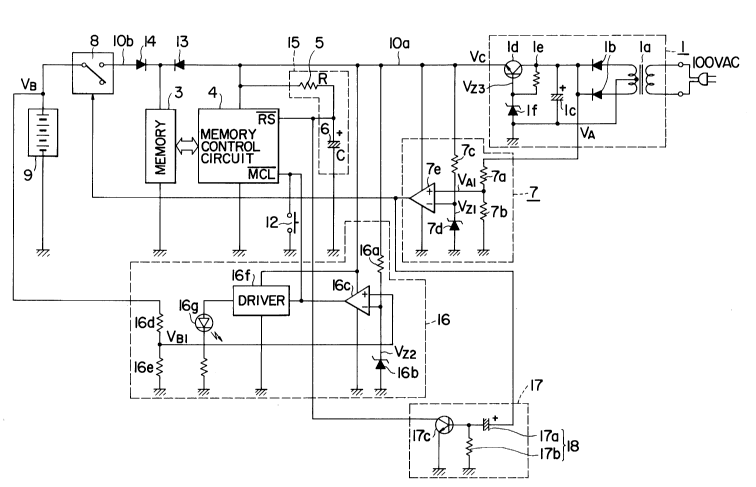
FIG. 2 is a block diagram showing an entire circuit
configuration of a memory drive device in accordance with
an embodiment of this invention. The same components as
those of the conventional device shown in FIG. 1 are
desig~ated by the same reference numrals, respectively.
7 21~3~
In FIG. 2, the stabilized power supply circuit 1
serving as the main power supply receives an AC voltage
of 100 V from the commercial power supply to output DC
regulator voltages VC and rectification voltages VA to
the main power supply line 10a and the power supply
voltage sense circuit 7, respectively.
The detailed description of the internal
configuration of the stabilized power supply circuit 1 is
as follows. Namely, the transformer la steps down an AC
voltage applied from the commercial power supply to a
predetermined value. The rectification circuit lb
applies full-wave rectification to an output from the
transformer la to convert it to a corresponding DC
voltage. The capacitor lc removes a ripple of the DC
voltage outputted from the rectification circuit lb to
form a substantially rectification voltage VA. The
control transistor ld receive at its base a constant
Zener voltage VZ3 generated by the Zener diode lf to
generate at its emitter a regulator voltage VC (= VZ3 -
VBE) to deliver it to the power supply line 10a.
When the backup power supply 9 is connected to thepower supply line 10b as a result of the fact that the
relay switch 8 is turned on, this power supply 9 delivers
a backup power to the memory 3 through the power supply
line 10b and the reverse-current prevention diode 14.
When an output voltage VA from the stabilized power
supply circuit 1 is lowered to a predetermined value, the
power supply voltage sense circuit 7 senses this, thus to
turn the relay switch 8 on.
The detailed description of the internal
configuration of the power supply voltage sense circuit 7
is as follows. Namely, the output voltage VA from the
stabilized power supply circuit 1 is voltage-divided by
resistors 7a, 7a. The divided voltage VAl thus obtained
is delivered to the non-inverting input terminal of the
comparator 7e. On the other hand, the Zener voltage VZl
generated by allowing a current to flow in the Zener
8, 2~132g6~
diode 7d through the resistor 7c is inputted to the
inverting input terminal of the comparator 7e. When the
comparator 7e receives.a power from the stabilized power
supply circuit 1 through the power supply line lOa, it is
driven to make a comparison between the divided voltage
VAl and the Zener voltage VZl. As a result, when the
divided voltage VAl is lower than the Zener voltage VZl,
the comparator 7e outputs a signal of which logic level
is "L". By this signal, the power supply changeover
switch 8 is switched to the power supply line lOb side.
The memory clear signal output circuit 16 checks
whether or not a backup voltage from the backup power
supply 9 is lowered at the time of recovery of service
interruption of the commercial power supply, or at the
time of memory backup. As a result, when lowering of the
backup voltage is sensed, the circuit 16 outputs a memory
clear signal of "L" level to the memory control circuit 4
to clear memory contents of the memory 3. The detailed
description of the internal configuration thereof is as
follows. Namely, a Zener voltage VZ2 caused by allowing
a current to flow in the Zener diode 16b through the
resistor 16a is inputted to the inverting input terminal
of the comparator 16c. Further, a voltage VBl obtained
by voltage-dividing an output voltage VB from the memory
backup power supply 9 by resistors 16d, 16e is applied to
the non-inverting input terminal of the comparator 16c.
~hen the comparator 16c receives a power from the
stabilized power supply circuit 1 through the power
supply line lOa, it is driven to output, to the memory
control circuit 4, a memory clear signal whose logic
level is "L" to clear memory contents in an initial
routine when the divided voltage VBl is lower than the
Zener voltage VZ2. This memory clear signal is also
delivered to the driver 16f for the light emitting diode
16g. The driver 16f becomes operative by a power
delivered from the power supply circuit 1 to turn the
light emitting diode 16g on and off when the memory clear
9 ~` 21~13;~9~i
signal is at "L" level, thereby notifying user of
dissipation of the backup power supply 9.
The reset signal output circuit 17 generates a reset
signal (RS) in response to the above-described memory
control circuit 4 by using the detection signal of a
power supply voltage detection circuit 7 that outputs a
detection signal after detecting that an output voltage
of the stabilized power supply circuit 1 reaches a
predetermined voltage.
At the time of recovery of service interruption, or
at the time of turning a power on, a rectification
voltage of the stabilized power supply circuit rises, and
when it is detected by the comparator 7e of the power
supply detection circui,t that a rectification voltage
divided by resistors 7a and 7b is higher than a Zener
voltage VZl, the output of the comparator 7e changes to a
high level.
In accordance with a rise in the output of the
comparator with increase in the output voltage of the
stabilized power supply circuit 1, a differential pulse
is formed at a differentiating circuit 18 of the reset
signal output circuit 17.
The pulse makes a transistor 17c conductive,
discharges a charge of a capacitor 6 in a time constant
circuit 15, and generates a negative pulse serving to
reset the memory control circuit 4 at the collector of
the transistor 17c in the reset signal output circuit 17.
The negative pulse further continues during a period
of continuity of the transistor 17c whose continuity
starts with the differentiation pulse. After continuity
of the transistor 17c is cut off, charging of the
capacitor 6 in the time constant circuit 15 starts. When
charging voltage rises higher than voltage that can
maintain reset for the memory control circuit 4 after a
rise in charging voltage from continued charge to the
capacitor 6, the memory control circuit 4 is released
from the reset.
lo 2(~32~
That is, when the output voltage of the stabilized
power supply circuit 1 rises in the process where the
power supply voltage rises up to a predetermined voltage
and the transistor 17c in the reset signal output circuit
17 becomes conductive by the output of the comparator 7
in the power supply detection circuit 7, electric
potential of the reset terminal in the memory control
circuit 4 falls, causing reset operation for the memory
control circuit 4.
The reset operation period depends on the time
constant determined by the capacitor 17a and the resistor
17b forming the differentiating circuit 18. After the
reset operation and lapse of a fixed period of time, the
transistor 17c is broken, causing the reset operation to
be released by a rise in the potential of the reset
terminal RS.
The memory control circuit 4 comprises, e.g., a
micro computer, executing an initial routine after the
reset operation. This initial routine monitors the logic
level of a memory clear signal terminal MCL in the memory
control circuit 4. The initial routine monitors logic
level of the memory clear signal terminal MCL in the
memory control circuit 4. When the logic level is
detected to be "L" level in the initial routine, the
memory control circuit 4 clears the contents of the
memory 3.
FIG. 3 is a waveform diagram showing voltage
waveform at each section in a process where an output
voltage value of the stabilized power supply circuit 1 at
time tO, rises to a predetermined value after recovery of
service interruption or the power supply is turned on.
The reset operation of the memory control circuit 4
and the clearing of the memory at the time of recovery of
service interruption are described with reference to FIG.
3.
In FIG. 3, when the power supply voltage is
recovered at time tO, the output VA serving as smoothing
11 2(~132~6
output of the stabilized powçr supply circuit 1 rises
gradually as shown in FIG. 3A. AS this voltage rises,
the capacitor 6 in the time-constant circuit 15 connected
to the reset terminal RS is progressively- charged,
causing the electric potential of the reset terminal RS
to rise in accordance with the time constant determined
by the capacitor 6 and the resistor 5 (shown in FIG. 3B).
When the smooth voltage VA of the stabilized power
supply circuit 1 rises and the smooth voltage VA divided
by the resistors 7a and 7b becomes:
R7b
R7a + Rtb
equalizing to the Zener voltage VZl, the output of the
power supply detection circuit 7 changes to a high level
as shown in FIG. 3C.
The reset signal output circuit 17 is connected to
the output terminal of the power suppIy voltage detection
circuit 7. The base potential of the transistor 17c
rises by the differentiating circuit 18 constituting the
reset signal output circuit at time t2 as shown in FIG.
3D, and then falls according to the time constant
determined by the capacitor 17a and resistor 17b
constituting the differentiating circuit 18.
The transistor 17c of the differentiating circuit 18
becomes conductive only during the period when its base
potential is higher than voltage VBE and continues
conductive during the period of time t2 to t4. During
the conductive period (time t2 to t4) of the transistor
17c, the level of the reset terminal RS is maintained at
a low level because a charge of the capacitor 6 is
discharged.
As a result, the memory control circuit 4 is reset
during the period of t2 to t4. In this case, because the
output VA of the stabilized power supply circuit
reaches a predetermined value at time t3, the memory
control circuit 4 is reset during the period of t3 to t4.
12 2(~1329~
The reset operation described above may be performed
during the period of t2 to t3 depending on how low the
- power supply voltage below a rated potential is when the
memory control circuit 4 starts normal operation.
The transistor 17c in the reset signal output
circuit 17 becomes a cut-off condition after time t4 and
the potential of the reset terminal RS rises in
accordance with the time constant in the time constant
circuit 15.
The potential of the-reset terminal RS further rises
and reset condition cannot be maintained at time t5. The
memory circuit 4 is released from reset condition.
That is, the memory control circuit 4 is reset after
the point a (time t2) in FIG. 3 and released at the point
b (time t5) from reset condition.
After completion of the resetting and reset-release
operations described above, the memory control circuit 4
executes an initial routine. In the initial routine, the
contents of the memory is cleared as required. In this
initial routine, the logic level of the memory clear
terminal MCL in the memory control circuit 4 is
monitored, and when the level is low, the contents of the
memory 3 is cleared. The memory clear signal is
generated by manual operation of the clear switch 12. On
the other hand, after the reset operation the signal is
automatically generated by the memory clear signal output
circuit 16 in the initial routine in the memory control
circuit 4.
In the memory clear signal output circuit 16, the
memory clear signal MCL is generated by comparing,
through the comparator 16c, the Zener voltage VZ2 on the
Zener diode 16b with a divided voltage VBl caused by
dividing voltage VB of the backup power supply 9 with
resistors 16d and 16e.
That is, when the batteries constituting the backup
power supply 9 is below the rated voltage due to power
dissipation and backs up the memory 3, the output of the
13 2~13Z96
comparator 16c is maintained at a low level to clear the
memory contents of the memory 3. In this case, the LED
blinks to show that power of the backup power supply 9
has dissipated.
When the output of the backup power supply 9 in
backup is, on the contrary, at a rated voltage, the
output of the comparator 16c is maintained at a high
level. Thus the memory is not cleared by the above-
mentioned initial routine.
The memory contents of the memory 3 is cleared by
manually pressing the clear switch 12 during the initial
routine.
While the scope of this invention is limited to the
above-described embodiment, this invention may be
modified in various manners within a range which does not
depart from the gist of the invention. For instance, the
reset signal output circuit 17 as shown in FIG. 4 may be
constructed with an one shot multivibrator 20 so that it
receives, on the trigger terminal thereof, an output from
the comparator 7e and is triggered by a rising edge in
that output, thus to generate a negative pulse of a fixed
time width, or as shown in FIG. 5, the reset signal
output circuit 17 may be constructed using a
retriggerable counter 22 so that it is triggered by a
rising edge of the output from the comparator 7e and
counts pulses from the clock 21 up to a fixed number,
outputting negative signals in count operation.