Note: Descriptions are shown in the official language in which they were submitted.
20 1 345 1
ADJACENT CHANNEL INTERFERENCE CANCELLER WITH
MEANS FOR MINIMIZING INTERSYMBOL INTERFERENCE
Background of the Invention:
This invention relates to a device such as an
adjacent channel interference canceller for processing a
device input signal carrying a digital symbol sequence
5 timed by a reference clock signal to produce a device
output signal to a demodulator. The demodulator
demodulates the device output signal into a reproduced
clock signal, a reproduced symbol sequence, and a
digital error signal. The reproduced clock signal is a
10 reproduction of the reference clock signal. The
reproduced symbol sequence is a reproduction of the
digital symbol sequence.
In general, a device of the type described is
supplied with a device input signal carrying the digital
15 symbol sequence. The device comprises a reception
filter for filtering the device input signal to produce
a filter output signal. The filter output signal has an
amplitude distortion resulting in a desired frequency
2 201 3451
band from adjacent interference on the desired frequency
band by one or two frequency bands adjacent to the
desired frequency band. The device serves to equalize
the amplitude distortion, as well known in the art.
A conventional device is disclosed in United
States Patent No. 4,333,063 issued to Toshihiko Ryu and
assigned to the instant assignee. According to Ryu, the
device comprises an adaptive amplitude equalizing unit
responsive to the filter output signal for equalizing
10 the amplitude distortion along a frequency axis of the
filter output signal to produce an amplitude equalized
signal as the device output signal.
The device input signal has an intermediate
level at a center of the desired frequency band. The
lS desired frequency band is adjacent to one or two other
frequency bands at sides of the other frequency bands.
The device input signal has side levels at the sides of
the desired frequency band. Therefore, the device input
signal inevitably includes the side levels as its level
20 components in two regions of the desired frequency band
that are adjacent to the other frequency bands.
It has now been found that intersymbol
interference is produced in the amplitude equalized
signal by over-suppression to the side levels on the
25 Ryu's adaptive amplitude equalizing unit. This is
because the side levels could not appropriately
suppressed by the reception filter.
20 1 345 1
3 64768-216
The device input signal has a decrease in the
intermedlate level when subjected to fading or the like. The side
levels are usually lower than the intermediate level.
When the decrease occurs, the side levels are
overestimated to be higher than the intermediate level. A~ a
result, the adaptive amplitude equalizing unit operatively over-
suppresses the æide levels to produce the amplitude equalized
æignal accompanied by the intersymbol interference.
SummarY of the Inventlon~
It is an object of thi~ invention to provide a device
capable of minimizing intersymbol interference produced by
oversuppression of side levels at the sides of a desired frequency
band.
According to a broad aspect of the invention there iB
provided a device for use in procesæing a device input signal
carrying a digital symbol sequence to produce a device output
signal, ~aid device comprising a reception filter for filtering
said device input signal to produce a filter output signal having
an amplitude distortion resultlng in a predetermined frequency
band from adjacent interference on said predetermined frequency
band by other frequency bands adjacent to said predetermined
frequency band, said amplitude distortion including a linear slope
distortion and a high order curvature distortion, the device
comprising 2
adaptive amplitude equalizing means including a slope
equalizer and a curvature equalizer, said ælope equalizer being
responsive to said filter output signal for equalizing said linear
slope distortion to produce a slope equalized signal, said
'~
:r
4 2 0 1 3 4 Sl 64768-216
curvature equalizer being responsive to said slope equalized
signal for equalizing said high order curvature distortion to
produce a first equalized signal having intersymbol interference;
and
adaptive transver~al equalizing means respon~ive to said
first equalized signal for equalizing said intersymbol
interference to produce a ~econd equalized signal as said device
output signal.
Brief DescrlPtion of the Dra~lng.
Figure 1 is a block diagram view of a device according
to an embodiment of the present invention;
Figure 2(a) ~hows a view of the spectrum of a device
input ~ignal;
Figure 2(b) shows a view of the spectrum of a filter
output signal;
Figure 2(c) shows a view of the spectrum of a first
equalized signal accompanied by intersymbol interference;
Figure 2(d) shows a view of the spectrum of a second
equalized signal with the intersymbol interference minimized;
Figure 3 is a block diagram view of an amplitude
controlling circuit used in the device of Figure l;
Figure 4 shows a view of characteri~tic curves of three
filters in the amplitude controlling circuit of Figure 3;
Figure 5 shows a block diagram view of an adaptive
transver~al equalizing unit and a demodulator used in the device
of Figure l; and
2~1 3~
_,
Fig. 6 shows a block diagram view of a
correlation detection circuit in the adaptive
transversal equalizing unit of Fig. 5.
Description of the Preferred Embodiments:
A device in accordance with the present
invention is supplied with a device input signal
subjected to modulation at a predetermined modulation
rate and produces a device output signal. The device
input signal carries a digital symbol sequence being
10 timed by a reference clock signal.
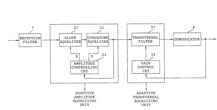
Referring to Fig. 1, the device comprises a
reception filter 1 supplied with the device input
signal, an adaptive amplitude equalizing unit 2, and an
adaptive transversal equalizing unit 3 for delivering
15 the device output signal to a demodulator 4.
The reception filter 1 is for filtering the
device input signal to deliver a filter output signal to
the adaptive amplitude equalizing unit 2.
Referring to Fig. 2(a), the device input signal
20 comprises a desired frequency band signal A and other
frequency band components B and C. The filter output
signal is the desired frequency band signal A and
accompanied with an amplitude distortion due to the
other frequency band components B and C, as shown in
25 Fig. 2(b). This is because the other frequency band
signals B and C could not be appropriately suppressed by
the reception filter 1.
6 20 ~ 3~ 1
The amplitude distortion comprises a linear
Slo,o~
shap~ distortion and a high order curvature distortion.
The linear slope distortion is determined by a linear
slope component and a slope polarity. The high order
5 curvature distortion includes a secondary curvature
distortion and the higher order ones. The high order
curvature distortion is determined by a high order
curvature component and a curvature polarity so that the
secondary curvature distortion is defined by a secondary
10 order curvature component and a curvature slope.
The following description will be made as
regards the linear slope distortion and the secondary
curvature distortion.
Returning to Fig. 1, the adaptive amplitude
15 equalizing unit 2 includes a slope equalizer 21 and a
curvature equalizer 22 cascaded thereto. The equalizers
21 and 22 can be designed to equalize the linear slope
distortion and the high order curvature distortion of
the filter output signal, respectively.
The filter output signal is applied to the slope
equalizer 21. The slope equalizer 21 equalizes the
linear slope distortion to produce a slope equalized
signal in response to a slope control signal X.
The slope equalized signal is applied to the
25 curvature equalizer 22. The curvature equalizer 22
equalizes the secondary curvature distortion in response
to a secondary curvature control signal Y. Then, the
curvature equalizer 22 provides a curvature equalized
- 2 0 1 3 45 1
signal as a first equalized signal to an amplitude
control circuit 23 and to the adaptive transversal
equalizing unit 3.
Referring to Fig. 3, the amplitude control
5 circuit 23 includes three narrow bandpass filters 10, 11
and 12 having respective center frequencies of (fO +
fl), (fO - fl) and fO, where fO is a center frequency of
the desired frequency band A and fl is a predetermined
frequency width. The center frequencies of (fO + fl)
10 and (fO - fl) are called side frequencies. The first
equalized signal from the curvature equalizer 22 is
applied in common to each of the bandpass filters 10,
11, and 12. The outputs from the bandpass filters 10,
11, and 12 are applied to three level detectors 13, 14,
15 and 15, respectively.
The outputs of the level detectors 13 and 14 are
applied to a non-inverting and an inverting inputs,
respectively, of a first differential amplifier 16 to
produce the linear slope component and the slope
20 polarity as the slope control signal X which is supplied
into the slope equalizer 21.
The outputs of the level detectors 13 and 14 are
coupled to a non-inverting input of a second
differential amplifier 17, through resistors 19 and 18,
25 respectively. The output of the level detector 15 is
applied to an inverting input of the second differential
amplifier 17 through a resistor 20 to produce the
secondary curvature component and the curvature polarity
8 201 3451
as the curvature control signal Y which is supplied into
the curvature equalizer 22.
Fig. 4 illustrates the amplitude vs. frequency
characteristics of the filters 10-12, W denoting a
5 bandwidth of the desired frequency band signal A.
The first differential amplifier 16 compares the
signal components of the side frequencies (fO + fl) and
(fO - fl) to detect the linear slope component and the
slope polarity thereof.
The second differential amplifier 17 compares
the signal component of the frequency (fO) and an
average value between the signal components of the side
frequencies (fO + fl) and (fO - fl) to detect the
secondary curvature component and the curvature polarity
15 thereof. If the adaptive amplitude equalizing unit 2 is
designed to equalize only the secondary or higher order
curvature components, the slope equalizer 21 and the
first differential amplifier 16 may be omitted.
L When the desired frequency band decreases by be~n~
- 20 subjected to fading, the signal component of the side
frequencies (fO + fl) and (fO - fl) are overestimated to
be higher than the signal component of the center
frequency (fO). As a result, the second differential
amplifier 17 detects an overestimated secondary
25 curvature component. Accordingly, the curvature
equalizer 22 operatively over-suppresses the signal
components of the side frequencies (fO + fl) and
9 201 3451
(f0 - fl) to produce the first equalized signal
accompanied by an intersymbol interference, as shown in
Fig. 2(c).
Referring to Figs. 1 and 5, the adaptive
5 transversal equalizing unit 3 is supplied with the first
equalized signal accompanied by the intersymbol
interference and comprises a transversal filter 31 for
filtering the first equalized signal IN into a second
equalized signal as the device output signal OUT in
10 response to a plurality of controllable tap gains which
may be specified by C(-l), C(0), and C(+l). The device
output signal OUT is also subjected to four-by-four
quadrature amplitude modulation like the first equalized
signal IN but is equalized by the transversal filter 31.
15 The illustrated transversal filter 31 has three taps. A
central one of the three taps may be called a central or
a first tap 33. The remaining ones of the taps are
depicted on the lefthand and the righthand sides of the
central tap 33 and may be called second and third taps
20 34 and 35, respectively. The second and the third taps
34 and 35 may be referred to as first and second
additional taps.
First and second delay units 36 and 37 are
placed between the second and the first taps 34 and 33
25 and between the first and the third taps 33 and 35,
respectively. Each of the first and the second delay
units 36 and 37 provides a delay which is substantially
equal to a reciprocal of the predetermined modulation
- 20 1 345 1
rate. The first equalized signal IN is delivered to the
second tap 34 as a first one of additional tap signals
and successively delayed by the first and the second
delay units 36 and 37 to be produced as a central tap
5 signal and a second additional tap signal which are sent
to the first and the third taps 33 and 35, respectively.
Let the second, the first, and the third taps
34, 33, and 35 be specified by consecutive numbers of
(-1), 0, and (+1), respectively, taking the successive
10 delays into consideration. In this connection, the
first additional tap signal appearing as the (-1) tap 34
may be specified by S(-l). Likewise, the central and
the second additional tap signals may be specified by
S(0) and S(+l), respectively.
Inasmuch as the first equalized signal IN is
subjected to over-suppression (referring to Fig. 2(c)),
the first equalized signal IN includes an in-phase and a
quadrature phase component. The in-phase and the
quadrature phase components are individually processed
20 with reference to the central tap signal S(0). More
specifically, the first additional tap signal S(-l) is
delivered to a first in-phase multiplier 41 and a first
quadrature multiplier 42. The second additional tap
signal S(+l) is delivered to a second in-phase
25 multiplier 43 and a second quadrature multiplier 44.
The central tap signal S(0) is given to a central
in-phase multiplier 45 alone because no quadrature phase
component is present in the central tap signal S(0).
20 1 34~ 1
11
Each of the multipliers 41 to 45 may be referred to as a
weighting circuit.
The controllable tap gains C(0), C(-l), and
C(+l) are produced by a gain control circuit 32 as will
S later be described in detail. The controllable tap
gains C(0), C(-l), and C(+l) may be referred to as a
central complex control signal, first and second complex
control signals, respectively.- The central complex
control signal C(0) consists of a real part alone and is
10 therefore represented by r(0) in Fig. 6. On the other
hand, each of the first and the second complex control
signals C(-l) and C(+l) consists of a real part and an
imaginary part represented by r and d, respectively. In
Fig. 5, the first complex control signal C(-l) is
15 specified by a combination of r(-l) and d(-l) while the
second complex control signal C(+l), a combination of
r(l) and d(l).
As shown in Fig. 5, the real and the imaginary
parts r(-l) and d(-l) of the first complex control
20 signal C(-l) are delivered from the gain control circuit
32 to the first in-phase and the first quadrature
multipliers 41 and 42, respectively. Likewise, the real
and the imaginary parts r(l) and d(l) of the second
complex control signal C(+l) are delivered to the second
25 in-phase and the second quadrature multipliers 43 and
44, respectively. The central complex control signal
C(0) or r(0) is sent to the central in-phase multiplier
45 in a usual manner.
12 2013~
The first in-phase and the first quadrature
multipliers 41 and 42 supply first and second adders 51
and 52 with a first controlled in-phase component S'(-l)
and a first controlled quadrature component S"(-l),
5 respectively. The second in-phase and the second
quadrature multipliers 43 and 44 supply the first and
the second adders 51 and 52 with a second controlled
in-phase component and a second controlled quadrature
component which are represented by S'(+l) and S"(+l),
10 respectively. Each of the first and the second in-phase
components may be named a first controlled signal while
each of the first and the second quadrature components
is named a second controlled signal. A central
controlled in-phase component S'(0) is sent from the
15 central in-phase multiplier 45 to the first adder 51.
The first and the second adders 51 and 52 carry
out addition to produce an in-phase signal RS and a
quadrature signal IS representative of results of the
addition, respectively. The in-phase and the quadrature
20 signals RS and IS may be called first and second
processed signals, respectively. In this connection,
the first and the second adders 51 and 52 may be
referred to as first and second processing circuits,
respectively. The in-phase and the quadrature signals
25 RS and IS are combined together by a coupling circuit 53
into a coupled signal with a quadrature phase relation
kept between the in-phase and the quadrature signals RS
13 2013451
and IS. The coupled signal is sent as the second
equalized signal OUT to a demodulator 4.
The demodulator 4 comprises a coherent detector
56 responsive to the second equalized signal OUT and to
5 a recovered carrier wave supplied from a carrier
recovery circuit 57. The coherent detector 56 carries
e red
out coherent detection with reference to the r^6~0v~rod
.. --.1
carrier wave to produce a demodulated baseband signal.
The demodulated baseband signal consists of an in-phase
10 and a quadrature component represented by Bp and Bq,
respectively. The in-phase and the quadrature
components Bp and Bq have an in-phase and a quadrature
level, respectively. Responsive to the in-phase and the
quadrature components Bp and Bq of the baseband signal,
15 a clock generator 59 delivers a reproduced clock signal
CLK to both of the gain control circuit 32 and a
discriminator 61. The reproduced clock signal CLK is a
reproduction of the reference clock signal. The
discriminator 61 produces a reproduced symbol sequence
20 D. The reproduced symbol sequence is a reproduction of
the transmission data sequence. The reproduced symbol
sequence D consists of in-phase symbol components Dp and
D'p and of quadrature symbol components Dq and D'q. The
in-phase symbol components Dp and D'p represent the
25 in-phase level of the in-phase component Bp of the
demodulated baseband signal. Likewise, the quadrature
symbol components Dq and D'q represent the quadrature
level of the quadrature component Bq of the demodulated
14 20 1 345 1
baseband signal. The discriminator 61 also produces a
digital error signal E. The digital error signal E is
related to the intersymbol interference. The digital
error signal E consists of an in-phase and a quadrature
5 error component Ep and Eq which correspond to the
in-phase and the quadrature symbol components Dp and Dq,
respectively.
The carrier recovery circuit 57 additionally
produces the recovered carrier wave in response to the
10 in-phase and the quadrature components Bp and Bq of the
demodulated baseband signal. The carrier recovery
circuit 57 is coupled to an asynchronous detection
circuit 62. The asynchronous detection circuit 62
monitors the carrier recovery circuit 57 to detect an
15 asynchronous state of the equalizer and to produce an
asynchronous state signal ASY representative of the
asynchronous state when the asynchronous detection
circuit 62 detects the asynchronous state.
The in-phase and the quadrature error components
20 Ep and Eq of the digital error signal E and the in-phase
and the quadrature symbol components Dp and Dq of the
reproduced symbol sequence D are delivered from the
demodulator 4 to the gain control circuit 32 together
with the reproduced clock signal CLK and the
25 asynchronous state signal ASY.
Responsive to the reproduced clock signal CLK,
to the in-phase and the quadrature error components Ep
and Eq of the digital error signal E, and to the
20 1 345 1
in-phase and the quadrature symbol components Dp and Dq
of the reproduced symbol sequence D, the gain control
circuit 32 controls the controllable tap gains C(j) by
the use of a zero forcing (ZF) algorithm where j
5 represents a tap number, such as 0, (-1), and (+1). It
will be assumed that a k-th time k is prior to a
(k+l)-th time (k+l) by a repetition period of the
reproduced clock signal CLK. According to the zero
forcing algorithm, controllable tap gains C(j, k+l) at
10 the (k+l)-th time (k+l) are decided by a combination of
a digital error signal E(k) at the k-th time k, a
reproduced symbol sequence D(k-j) at a (k-j)-th time
(k-j), and controllable tap gains C(j, k) at the k-th
time k as follows:
H
C(j, k+l) = C(j, k) - a[sgn{ ~ D*(k-j) x E(k)}] (1)
C(j, k) = r(j)(k) + id(j)(k) (2)
E(k) = Ep(k) + iEq(k) (3)
20 D*(k-j) = Dp(k-j) - iDq(k-j) (4)
where ~ represents a fixed incremental step size, i
represents an imaginary unit which is equal to ~ , the
notation "sgn" represents a polarity of the argument
enclosed with a pair of braces, H represents a positive
25 integer.
The controllable tap gains C(j, k+l) have real
and imaginary parts r(j, k+l) and d(j, k+l) which are
given by:
16 20 1 3~5 1
r(j, k+l) = r(j, k) - arsgn{ ~ (Ep(k) ~ Dp(k-j)
k=1
+ Eq(k) ~ Dq(k-j))~] (S)
S H
d(j, k+l) d(j, k) a[sgn~k~l(Eq(k) ~ Dq(k j)
+ Ep(k) ~ Dq(k-j))}] (6)
where the symbol ~ is used as an Exclusive-OR operator
10 and the symbol ~ is used as an Exclusive-NOR operator.
The gain control circuit 32 comprises a
correlation detecting circuit 63 and an integrating
circuit 64. The correlation detecting circuit 63 is for
finding out cross-correlation between the reproduced
15 symbol sequence D(m) and the digital error signal E(m)
to produce a plurality of correlation signals. The
integrating circuit 64 is for integrating the
correlation signals to produce a plurality of integrated
signals as the controllable tap gains C(j).
Referring to Fig. 6, the correlation detecting
circuit 63 comprises a delaying circuit 65 and an
Exclusive logic circuit 70. The delaying circuit 65 is
for delaying the reproduced symbol sequence D(m) and the
digital error signal E(m) to produce a delayed symbol
25 sequence D(m-l) and a delayed error signal E(m-l) in
synchronism with the reproduced clock signal CLK. The
delayed symbol sequence D(m-l) and the delayed error
signal E(m-l) are delayed by one repetition period of
the reproduced clock signal CLK relative to the
30 reproduced symbol sequence D(m) and the digital error
17 201 3451
signal E(m), respectively. More particularly, the
delaying circuit 65 comprises first through fourth flip
flops 66, 67, 68, and 69. The delayed clock signal CLK
is delivered to the flip flops 66 through 69. The first
5 flip flop 66 is for delaying an in-phase error component
Ep(m) of the digital error signal E(m) to produce a
delayed in-phase error component Ep(m-l) of the delayed
error signal E(m-l) in synchronism with the reproduced
clock signal CLK. Likewise, the second flip flop 67 is
10 for delaying a quadrature error component Eq(m) of the
digital error signal E(m) to produce a delayed
quadrature error component Eq(m-l) of the delayed error
signal E(m-l) in synchronism with the reproduced clock
signal CLK. The third and the fourth flip flops 68 and
15 69 are for delaying in-phase and quadrature symbol
components Dp(m) and Dq(m) of the reproduced symbol
sequence D(m) to produce delayed in-phase and delayed
quadrature symbol components Dp(m-l) and Dq(m-l) of the
delayed symbol sequence D(m-l), respectively, in
20 synchronism with the reproduced clock signal CLK.
The delayed symbol sequence D(m-l), the delayed
error signal E(m-l), the reproduced symbol sequence
D(m), and the digital error signal E(m) are supplied to
the Exclusive logic circuit 70 as a plurality of input
25 signals. The Exclusive logic circuit 70 is for carrying
out an exclusive logic operation on the input signals to
produce the correlation signals. The Exclusive logic
circuit 70 comprises first through ninth Exclusive-OR
-
18 20 1 345 1
gates 71, 72, 73, 74, 75, 76, 77, 78, and 79, and first
through third Exclusive-NOR gates 81, 82, and 83. More
particularly, the first Exclusive-OR gate 71 carries out
an exclusive OR operation on the in-phase error
5 component Ep(m) and the in-phase symbol component Dp(m)
to produce a first correlation signal Pr(0). Therefore,
the first correlation signal Pr(0) is given by:
Pr(0) = Ep(m) ~ Dp(m).
Similarly, the second Exclusive-OR gate 72 carries out
10 an exclusive OR operation on the quadrature error
component Eq(m) and the quadrature symbol component
Dq(m) to produce a second correlation signal Qr(0). The
second correlation signal Qr(0) is given by:
Qr(0) = Eq(m) ~ Dq(m).
15 Likewise, the third Exclusive-OR gate 73 carries out an
exclusive OR operation on the quadrature error component
Eq(m) and the in-phase data component Dp(m) to produce a
third correlation signal Qd(0). The third correlation
signal Qd(0) is given by:
Qd(0) = Eq(m) ~ Dp(m).
The first Exclusive-NOR gate 81 carries out an exclusive
NOR operation on the in-phase error component Ep(m) and
the quadrature symbol component Dq(m) to produce a
fourth correlation signal Pd(0). The fourth correlation
25 signal Pd(0) is given by:
Pd(0) = Ep(m) ~ Dq(m).
In this manner, the fourth, the fifth, and the
sixth Exclusive-OR gates 74, 75, and 76, and the second
-
19 20 1 345 1
Exclusive-NOR gate 82 produce fifth, sixth, seventh, and
eighth correlation signals Pr(-l), Qr(-l), Qd(-l), and
Pd(-l) which are given by:
Pr(-l) = Ep(m-l) ~ Dp(m),
Qr(-l) = Eq(m-l) ~ Dq(m),
Qd(-l) = Eq(m-l) ~ Dp(m),
and Pd(-l) = Ep(m-l) ~ Dq(m).
Similarly, the seventh, the eighth, and the
ninth Exclusive-OR gates 77, 78, and 79, and the third
10 Exclusive-NOR gate 83 produce ninth, tenth, eleventh,
and twelfth correlation signals Pr(l), Qr(l), Qd(l), and
Pd(l) which are given by:
Pr(l) = Ep(m) ~ Dp(m-l),
Qr(l) = Eq(m) ~ Dq(m-l),
Qd(l) = Eq(m) ~ Dp(m-l),
and Pd(l) = Ep(m) ~ Dq(m-l).
The correlation signals except for the third and
the fourth correlation signals Qd(0) and Pd(0) are
supplied to the integrating circuit 64.
Although the in-phase and the quadrature
components Bp and Bq of the demodulated baseband signal
are supplied to the carrier recovery circuit 57 as
mentioned above, the in-phase and the quadrature
components Bp and Bq of the demodulated baseband signal
25 may not be always supplied to the carrier recovery
circuit 57. In this case, the third and the fourth
correlation signals Qd(0) and Pd(0) is used instead of
20 1 345 1
the in-phase and the quadrature components Bp and Bq of
the demodulated baseband signal.
Turning back to Fig. 5, the integrating circuit
64 comprises first through fifth resettable integrators
5 91, 92, 93, 94, and 95. The first resettable integrator
91 is coupled through first and second registers 101 and
102 to the first and the second Exclusive-OR gates 71
and 72. Similarly, the second resettable integrator 92
is coupled through third and fourth registers 103 and
10 104 to the fourth and the fifth Exclusive-OR gates 74
and 75. The third resettable integrator 93 is coupled
through fifth and sixth registers 105 and 106 to the
sixth Exclusive-OR gate 76 and the second Exclusive-NOR
gate 82. The fourth resettable integrator 94 is coupled
15 through seventh and eighth registers 107 and 108 to the
seventh and eighth Exclusive-OR gates 77 and 78. The
fifth resettable integrator 95 is coupled through ninth
and tenth registers 109 and 110 to the ninth Exclusive-
OR gate 79 and the third Exclusive-NOR gate 83.
A pair of the first and the second registers 101
and 102 are for combining the first correlation signal
Pr(0) and the second correlation signal Qr(0) to produce
a first combined signal ER(0). Therefore, the first
combined signal ER(0) is given by:
ER(0) = Pr(0) + Qr(0)
= Ep(m) ~ Dp(m) + Eq(m) ~ Dq(m).
Similarly, another pair of the third and the fourth
registers 103 and 104 are for combining the fourth
20 1 345 t
21
correlation signal Pr(-l) and the fifth correlation
signal Qr(-l) to produce a second combined signal ER(-l)
which is given by:
ER(-l) = Pr(-l) + Qr(-l)
= Ep(m-l) ~ Dp(m) + Eq(m-l) ~ Dq(m).
In this manner, pairs of the fifth and the sixth
registers 105 and 106, the seventh and the eighth
registers 107 and 108, and the ninth and the tenth
registers 109 and 110 produce third, fourth, and fifth
10 combined signals EI(-l), ER(l), and EI(l), respectively,
which are given by:
EI(-l) = Qd(-l) + Pd(-l)
= Eq(m-l) ~ Dp(m) + Ep(m-l) ~ Dq(m),
ER(l) = Pt(l) + Qr(l)
= Ep(m) ~ Dp(m-l) + Eq(m) ~ Dq(m-l),
and EI(l) = Qd(l) + Pd(l)
= Eq(m) ~ Dp(m-l) + Ep(m) ~ Dq(m-l).
The first through the fifth resettable
integrators 91 to 95 are coupled to the asynchronous
20 detecting circuit 62. When the asynchronous state
signal ASY is given from the asynchronous detecting
circuit 62 to the first through the fifth resettable
integrators 91 to 95, the first resettable integrators
91 is reset into a logic "1" level and is kept at the
25 logic "1" level. Each of the remaining integrators 92
to 95 is reset into a logic "0" level. In the absence
of the asynchronous state signal ASY, each of the
integrators 91 to 95 works out a time average of each
22 201 3451
combined signal ER(0), ER(-l), EI(-l), ER(l), and EI(l)
to remove an unnecessary noise component from each
combined signal. Anyway, the first through the fifth
integrators 92 to 95 produce the controllable tap gains
5 C(0), C(-l), and C(+l).
The first through the tenth registers 101 to 110
are for use in combining each pair of the correlation
signals as mentioned above. However, OR gates may be
used instead of the first through the tenth registers
10 101 to 110.
Referring:to Fig. 2(d), it will be understood
that the adaptive transversal equalizing unit 3 is
operable of minimizing the intersymbol interference.
Therefore, the device according to this invention can
15 cancel all distortion due to the adjacent channel
interference.