Note: Descriptions are shown in the official language in which they were submitted.
t,
TITLE OF THE INVENTION
Synchronizing Signal Separating Circuit
BACKGROUND OF THE INVENTION
Field of the Invention
The present invention relates generally to
synchronizing signal separating circuits, and more
particularly, to a synchronizing signal separating circuit
for separating a synchronizing signal from a composite
video signal in a circuit of, for example, a chrominance
signal processing system, a deflection system or the like
in a video apparatus such as a television (TV) receiver, a
video tape recorder (VTR) and a video disc player.
Description of the Background Art
Conventionally, in a video apparatus such as a TV
receiver, a VTR and a video disc player, for use in
various operations a horizontal synchronizing signal and a
vertical synchronizing signal are separated from an
inputted or reproduced composite video signal and supplied
to various circuits, such as a chrominance signal
processing circuit and a deflection circuit in the video
apparatus.
Fig. 1 is a circuit diagram showing one example of
such a conventional synchronizing signal separating
circuit, in case it is applied, for example, to a TV
receiver. More specifically, a composite video signal
received by an antennae and a video receiving circuit
which are not shown is amplified in a video amplifying
circuit 100 and then, supplied to a synchronizing signal
separating circuit 200. The synchronizing signal
separating circuit 200 extracts a horizontal synchronizing
signal and a vertical synchronizing signal from the
applied composite video signal and outputs the same as a
composite synchronizing signal. The composite
synchronizing signal outputted from the synchronizing
signal separating circuit 200 is supplied, for example, to
a deflection circuit 300, wherein the signal is further
separated into a horizontal synchronizing signal and a
vertical synchronizing signal for use in a deflecting
operation.
Described in more detail on the synchronizing signal
separating circuit 200 of Fig. 1, an output of the video
amplifying circuit 100 is supplied to a positive input of
a comparator 2 through a coupling condenser 1. In
addition, a reference voltage of e.g. 2.5V is applied to a
negative input of the comparator 2. An output of the
comparator 2, after being inverted by an inverter 3, is
supplied as a composite synchronizing signal to a
deflection circuit 300, and also it is further inverted by
an inverter 4 and then supplied to gates of a p-channel
MOSFET 5 and an n-channel MOSFET 6. These MOSFETs and
- 2 -
bias resistors 7 and 8 are connected in series between a
power supply potential Vcc and a ground potential, and a
node of the resistors 7 and 8 is further connected to the
positive input of the comparator 2.
Now, Fig. 2 is a waveform diagram for explaining an
operation of the synchronizing signal separating circuit
100 shown in Fig. 1, wherein Figs. 2 (A), (B), (C) and (D)
show signal waveforms approximately in one horizontal
period at the corresponding nodes A, B, C and D in the
circuit of Fig. 1.
First, when a composite video signal shown in Fig. 2
(A) is applied to the positive input of the comparator 2
through the coupling condenser 1, the comparator 2
compares the composite video signal with the reference
potential applied to the negative input (a dashed line~of
Fig. 2 (A)) and amplifies the result, and outputs a
horizontal synchronizing signal of a negative polarity as
shown in Fig. 2 (B) to supply the same to the inverter 3.
The horizontal synchronizing signal inverted by the
inverter 3 becomes a signal of a positive polarity as
shown in Fig. 2 (C), and is supplied to the deflection
circuit 300 in the succeeding stage and also supplied to
the inverter 4 wherein it is further inverted. The
inverter 4 outputs a horizontal synchronizing signal of
the negative polarity as shown in Fig. 2 (D) and supplies
- 3 -
the same to the gates of the p channel MOSFET 5 and n
channel MOSFET 6.
As a result, in a horizontal synchronizing signal
period of Fig. 2 (D), the p channel MOSFET 5 is turned on
and the n channel MOSFET 6 is turned off, so that the
coupling condenser 1 is charged with the electric charges
from the power supply Vcc through the bias resistor 7, and
in the period except the horizontal synchronizing signal
period, the p channel MOSFET 5 is turned off and the n
channel MOSFET 6 is turned on, so that the electric
charges stored in the coupling condenser 1 are discharged
through the bias resistor 8. A ratio of a length of a
horizontal synchronizing signal period to a length of the
other period in one horizontal period is defined as about
1:12, and corresponding thereto, a ratio of a resistance
value of the bias resistor 7 to that of the bias resistor
8 is set at about 12:1. As a result, the amount of
electric charges to be charged in the coupling condenser 1
and that of electric charges to be discharged therefrom
become equal, whereby a horizontal synchronizing signal is
correctly separated.
The destination of thus separated horizontal
synchronizing signal (Fig. 2 (C)) is not limited to the
deflection circuit 300 shown in Fig. 1, but it can be
supplied to any circuit requiring a synchronizing signal
- 4 -
~t~~~
such as a chrominance signal processing circuit in the
video apparatus. In addition, while the inverters 3 and 4
are provided in case a horizontal synchronizing signal to
be required is of the positive polarity, in case such a
horizontal synchronizing signal of the negative polarity
as shown in Fig. 2 (B) is required, they are not
necessary, and it may be constituted so as to supply the
output of the comparator 2 as a horizontal synchronizing
signal. In addition, while the foregoing description is
on the operation in case the horizontal synchronizing
signal is separated in a manner as shown in Fig. 2, since
a vertical synchronizing signal is comprised of a
plurality of pulses each having the above described time
ratio of 1:12, it can be separated in the circuit of Fig.
1 similarly to the horizontal synchronizing signal.
As the foregoing, the synchronizing signal separating
circuit using MOSFETs is disclosed in, for example,
Japanese Patent Laying Open Nos. 56-80965, 58-60880 and
61-198977.
In the conventional synchronizing signal separating
circuit shown in Fig. 1, the coupling condenser 1 is
charged with a fixed amount of electric charges from the
power supply Vcc through the bias resistor 7 in the
synchronizing signal period. When there exist a very
bright portion and a very,dark portion in a picture frame,
- 5 -
2013532
an average picture level (APL) of a video signal becomes
significantly different in each horizontal period in some
cases. For example, Fig. 3 (A) indicates that one
horizontal line includes a lot of white portions to cause
the APL to become high and Fig. (B) indicates that one
horizontal line includes a lot of black portions to cause
the APL to become low. Accordingly, if the coupling
condenser 1 is always charged with a fixed amount of
electric charges with respect to video signals in
horizontal periods in which the APLs thereof are
different, a signal level supplied to the positive input
of the comparator 1 falls or rises with respect to a fixed
separation level (dashed line of Fig. 3) supplied to the
negative input of the comparator 2. As a result, when the
separation level becomes contiguous to a lower end or an
upper end of a synchronizing signal, noise,-a burst signal
or the like on the video signal is erroneously detected as
a synchronizing signal in some cases and then outputted,
so that various processings using a synchronizing signal
can not be performed normally.
SUMMARY OF THE INVENTION
Therefore, an object of the present invention is to
provide a synchronizing signal separating circuit capable
of correctly separating a synchronizing signal from a
composite video signal.
- 6 -
2013532
Another object of the present invention is to provide
a synchronizing signal separating circuit which does not
erroneously detect noise, a burst signal or the like in a
composite video signal as a synchronizing signal.
A further object of the present invention is to
provide a synchronizing signal separating circuit capable
of maintaining a difference in level between a top level
of a synchronizing signal and a separation level to be
constant, irrespective of an APL of an inputted video
signal.
Briefly stated, the present invention is a
synchronizing signal separating circuit for separating a
synchronizing signal from an inputted signal including at
least a synchronizing signal, and the circuit comprises a
coupling condenser for receiving an inputted signal, an
inverter for inverting and amplifying the input signal
received through the coupling condenser, a limiter for
limiting an amplitude of an output signal of the inverter
to supply the output signal having its amplitude limited
as the synchronizing signal, a first bias resistor for
connecting an output node to an input node of the inverter
to charge the coupling condenser with an output signal of
the inverter, a switch provided between the output node of
the inverter and the first bias resistor and being
controlled so as to be turned on in a synchronizing signal
2013532
period in response to an output signal of the limiter,
and a second bias resistor provided between the input
node of the inverter and a ground potential for
discharging electric charges of the coupling condenser.
Accordingly, in one of its aspects, the present
invention provides a synchronizing signal separating
circuit for separating, from an input signal including
at least a synchronizing signal, said synchronizing
signal, comprising: coupling capacitance means (1) for
receiving said input signal, first inverting and
amplifying means (12) for inverting and amplifying said
input signal received through said coupling capacitance
means, first limiter means (13) for limiting an
amplitude of an output signal of said first inverting
and amplifying means to supply said output signal having
its amplitude limited as said synchronizing signal,
first bias means (10) for connecting an output node (B)
to an input node (A) of said first inverting and
amplifying means for charging said coupling capacitance
means with the output signal of said first inverting and
amplifying means, first switching means (14) provided
between the output node of said first inverting and
amplifying means and said first bias means and being
controlled so as to be turned on in said synchronizing
signal period in response to the output signal of said
first limiter means and, second bias means connected
between the input node of said first inverting and
_ g _
2013532
amplifying means and a fixed reference potential for
discharging electric charges of said coupling
capacitance means.
In a further aspect, the present invention relates
to a synchronizing signal separating circuit for
separating, from an input signal including at least a
synchronizing signal, said synchronizing signal,
comprising: coupling capacitance means (1) for receiving
said input signal, first inverting and amplifying means
(12) for inverting and amplifying said input signal
received through said coupling capacitance means,
comparing means (15) for comparing input and output
signals of said first inverting and amplifying means to
supply the result of comparison as said synchronizing
signal, first bias means (10) for connecting an output
node (B) to an input node (A) of said first inverting
and amplifying means for charging said coupling
capacitance means with the output signal of said first
inverting and amplifying means, first switching means
(14) provided between the output node of said first
inverting and amplifying means and said first bias means
and being controlled so as to be turned on in said
synchronizing signal period in response to the output
signal of said comparing means and, second bias means
(11) connected between the input node of said first
inverting and amplifying means and a fixed reference
- 8a -
2013532
potential for discharging electric charges of said
coupling capacitance means.
In a still further aspect, the present invention
relates to a synchronizing signal separating system
comprising a first (600) and a second (700)
synchronizing signal separating circuit each including
coupling capacitance means (1, 28) for receiving an
input signal, first inverting and amplifying means (12,
33) for inverting and amplifying said input signal
received through said coupling capacitance means (1,
28), first limiter means (13, 35) for limiting an
amplitude of an output signal of said first inverting
and amplifying means (12, 33) to supply said output
signal having its amplitude limited as said
synchronizing signal, characterized in that said first
and second synchronizing signal separating circuits
further comprise first bias means (10, 32) for
connecting respective output nodes (B, F) to respective
input nodes (A, E) of the respective first inverting and
amplifying means (12, 33) for charging said respective
coupling capacitance means (1, 28) with the output
signal of said respective first inverting and amplifying
means (12, 33), first switching means (14, 34) provided
between the output nodes of said first inverting and
amplifying means and said first bias means and being
controlled so as to be turned on in said synchronizing
signal period in response to the output signal of said
- 8b -
2013532
respective first limiter means, second bias means (11,
29) connected between the respective input nodes (A, E)
of said first inverting and amplifying means (12, 33)
and fixed reference potentials for discharging electric
charges of said respective coupling capacitance means
(1, 28) wherein said first synchronizing signal
separating circuit (600) further includes an OR-gate
(36) for receiving a pseudo-horizontal synchronizing
signal and a pseudo-vertical synchronizing signal, and
AND-gate (37) for receiving an output of said OR-gate
(36) and a synchronizing determining signal, a second
inverting and amplifying means (39) for inverting the
output of said first limiter means (13) and a NOR-gate
(38) for receiving the output of said AND-gate (37) and
the output of the second inverting and amplifying means
(39), wherein the output of said NOR-gate is supplied as
control input of said first switching means (14), said
second synchronizing signal separating circuit (700)
further includes said bias means (30) and second
switching means (311 connected in series between said
input node (E) and the reference potential, in parallel
with said second bias means (29), a switching of said
second switching means being controlled so as to be
turned on in the vertical synchronizing signal period,
wherein the first synchronizing signal separating
circuit (600) receives a composite video signal to
separate a composite synchronizing signal including a
- 8c -
2013532
horizontal synchronizing signal and a vertical
synchronizing signal, and wherein the second
synchronizing signal separating circuit (700) receives a
composite synchronizing signal, separated from the
composite video signal by said first synchronizing
signal separating circuit (600), to separate only the
vertical synchronizing signal.
Therefore, a principal advantage of the present
invention is that even if a composite video signal
having a different APL is inputted, a level difference
between a top level of a synchronizing signal and a
separation level does not change, whereby the
synchronizing signal can be correctly separated.
The foregoing and other objects, features, aspects
and advantages of the present invention will become more
apparent from the following detailed description of the
present invention when taken in conjunction with the
accompanying drawings.
BRIEF DESCRIPTION OF THE DRAWINGS
Fig. 1 is a circuit diagram showing one example of
a conventional synchronizing signal separating circuit.
Figs. 2 and 3 are timing charts for explaining an
operation of the synchronizing signal separating circuit
shown in Fig. 1.
Fig. 4 is a circuit diagram showing a synchronizing
signal separating circuit according to a first
embodiment of the present invention.
- 8d -
Figs. 5 and 6 are timing charts for explaining an
operation of the embodiment shown in Fig. 4.
Fig. 7 is a circuit diagram showing a synchronizing
signal separating circuit according to a second embodiment
of the present invention.
Fig. 8 is a timing chart for explaining an operation
of the embodiment shown in Fig. 7.
Fig. 9 is a circuit diagram showing a synchronizing
signal separating circuit according to a third embodiment
of the present invention.
Fig. 10 is a schematic block diagram showing a
horizontal AFC circuit.
Figs. 11, 12 and 13 are timing charts for explaining
an operation of the embodiment shown in Fig. 9. .
Figs. 14 anc~ 15 are circuit diagrams showing modified
examples of the embodiment shown in Fig. 4.
DESCRIPTION OF THE PREFERRED EMBODIMENTS
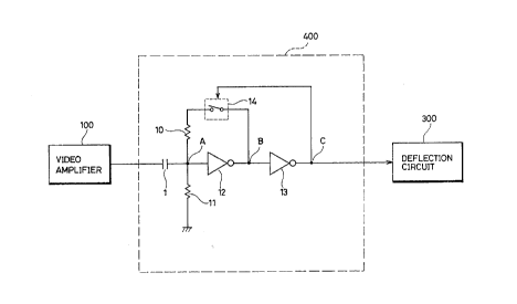
Fig. 4 is the circuit diagram showing the
synchronizing signal separating circuit according to the
first embodiment of the present invention. Referring to
Fig. 4, an output of a video amplifying circuit 100 is
supplied to a synchronizing signal separating circuit 400,
wherein it is supplied to an input of an inverter 12
through a coupling condenser 1. An output of the inverter
12 is supplied to an input of an inverter 13 and also
_ 9 _
201~53~
supplied to an input node A of the inverter 12 through a
switch 14 and a bias resistor 10 connected in series. The
input node A is grounded through a bias resistor 11. An
output of the inverter 13 is supplied as a composite
synchronizing signal to a deflection circuit 300 and also
supplied as a control signal to the switch 14 to control
the switching of the switch 14.
Fig. 5 is the waveform diagram for explaining an
operation of the synchronizing signal separating circuit
400 shown in Fig. 4, wherein Figs. 5 (A), (B) and (C) show
signal waveforms approximately in one horizontal period at
the corresponding nodes A, B and C in the circuit of Fig.
4, respectively. A dashed line in Fig. 5 indicates a
threshold level of the inverters 12 and 13.
First, when the composite video signal shown in Fig.
5 (A) is supplied to the input of the inverter 12 through
the coupling condenser 1, the inverter 12 inverts and
amplifies the composite video signal to output such a
signal as shown in Fig. 5 (B) and then supplies the signal
to the input of the inverter 13 and also to the input node
A of the inverter 12 through the switch 14 and the bias
resistor 10. The inverter 13 inverts and amplifies the
supplied signal to output such a horizontal synchronizing
signal of a negative polarity as shown in Fig. 5 (C) and
then supplies the same to the deflection circuit 300.
- 10 -
2013532
Namely, the inverter 13 functions as a limiter. The
horizontal synchronizing signal outputted from the
inverter 13 is supplied also to the control input of the
switch 14.
The switch 14 is constituted so as to be turned on
while a control signal is at an "L" level and turned off
while it is at an "H" level. Accordingly, in a horizontal
synchronizing signal period (during an "L" level period of
Fig. 5 (C)) the switch 14 is turned on, so that the
coupling condenser 1 is charged with the amount of
electric charges corresponding to a voltage indicated by V
in Fig. 5 (B) through the bias resistor 10. On the other
hand, in other period ("H" level period of Fig. 5 (C))
than the horizontal synchronizing signal period, the
switch 14 is turned off, so that the electric charges
stored in the coupling condenser 1 are discharged through
the bias resistor 11.
As the foregoing, if it is constituted such that the
coupling condenser 1 is charged with the amount of
electric charges corresponding to the voltage V shown in
Fig. 5 (B), when a composite video signal having an APL
fluctuating in each horizontal period as shown in Fig. 6
is inputted, although the inputted signal level fluctuates
with respect to the threshold level as described in the
foregoing, the voltage V also fluctuates correspondingly.
- 11 -
2fl13S32
For example, if the separation level becomes contiguous to
the lower end of the horizontal synchronizing signal, the
voltage V becomes small and the amount of electric charges
to be charged decreases, so that the separation level is
shifted upward. On the contrary, if the separation level
becomes contiguous to the upper end of the horizontal
synchronizing signal, the voltage V becomes large and the
amount of the electric charges to be charged increases, so
that the separation level is shifted downward. Namely,
since a direct current bias at the node A fluctuates in
each horizontal period, even if the composite video signal
having an APL fluctuating in each period as shown in Fig.
6 is inputted, a level difference between a top level of
the horizontal synchronizing signal and a separation
level, that is, a threshold level of the inverter is
maintained to be constant. As a result, in the
synchronizing signal separating circuit of Fig. 4, it is
not possible that a separation level becomes contiguous to
a lower end or an upper end of a synchronizing signal, so
that no noise or a burst signal is erroneously'detected as
the synchronizing signal, as is the case with the
conventional synchronizing signal separating circuit of
Fig. 1.
In the embodiment of the Fig. 4, the larger a ratio
of a resistance value of the bias resistor 11 to a
- 12 -
20~.~53~
resistance value of the bias resistor 10 becomes, the more
separation sensitivity of the synchronizing signal
separating circuit is improved. Namely, the resistance
value of the bias resistor 11 larger than that of the bias
resistor 10 causes the separation level to near the lower
end of the synchronizing signal. As a result, separation
of the synchronizing signal becomes less susceptible to
the video signal, thereby the separation sensitivity is
improved. However, it is important not to allow the
separation level to near the lower end too much because
the separation of the synchronizing signal is affected by
noise included in a horizontal synchronization period in a
weak electric field. In addition, increased gain of the
inverter 12 causes the voltage V to be increased, whereby
the amount of electric charge to be charged is also
increased. This also enables the separation level to near
the lower end of the synchronizing signal to improve the
separation sensitivity.
Fig. 7 is the circuit diagram showing the
synchronizing signal separating circuit according to the
second embodiment of the present invention. A basic
configuration of a synchronizing signal separating circuit
500 shown in Fig. 7 is the same as that of the
synchronizing signal separating circuit 400 according to
the first embodiment shown in Fig. 4 except for the
- 13 -
201~53~
following points. Namely, a comparator 15 is provided in
place of the inverter 13, for comparing the output and the
input of the inverter 12, the output of the inverter 12 is
taken out through separately provided low pass filter
(LPF) 16 and inverter 21, and series-connected bias
resistor 23 and switch 22 are provided between the node A
and the ground, in parallel with the bias resistor 11.
The above described LPF 16 is comprised of an inverter 18,
a condenser 19 and a resistor 20 and has an output
supplied to a synchronization determining circuit (not
shown) through the inverter 21. In addition, the output
of the inverter 17 is supplied to a horizontal automatic
frequency control (AFC) circuit for use as a chrominance
signal processing circuit or the like. Switching of the
switch 22 is controlled by a vertical equalizing pulse
extracted in a vertical synchronizing signal separating
circuit (not shown) provided in a stage subsequent to, for
example, this synchronizing signal separating circuit.
The inverters 24 and 17 may be suitably provided as
required in order to obtain the synchronizing signal of
the desired polarity.
Fig. 8 is a waveform diagram for explaining an
operation of the synchronizing signal separating circuit
500 shown in Fig. 7, wherein Figs. 8 (A), (B), (C) and (D)
show signal waveforms approximately in one horizontal
- 14 -
2013532
period at the corresponding nodes A, B, C and D in the
circuit of Fig. 7, respectively.
First, when a composite video signal shown in Fig. 8
(A) is supplied to the input of the inverter 12 through
the coupling condenser 1, the inverter 12 inverts and
amplifies the signal to output such a signal as shown in
Fig. 8 (B) and then supplies the signal to a positive
input of the comparator 15 and also to the input node A of
the inverter 12 through the switch 14 and the bias
resistor 10. In addition, the output of the inverter 12
is supplied also to the inverter 21 through the LPF 16.
On the other hand, the signal of the node A (Fig. 8 (A))
is supplied to a negative input of the comparator 15, so
that the comparator 15 outputs a horizontal synchronizing
signal of the positive polarity shown in Fig. 8 (C) to the
node C. The output of the comparator 15 is inverted and
amplified by the inverter 13 to become such.a horizontal
synchronizing signal of the negative polarity as shown in
Fig. 8 (D) and then the signal is supplied to the control
input of the switch 14 and also to, for example, a
horizontal AFC circuit (not shown) through the inverter
17. On this occasion, the switch 14 is a switch which is
turned on during the control signal is at the "L" level
and turned off during it is at the "H" level, as described
above. Accordingly, in the horizontal synchronizing
- 15 -
20~~532
signal period (in the "L" level period of Fig. 8 (D)) the
switch 14 is turned on, so that the coupling condenser 1
is charged by a potential of the node B through the bias
resistor 10, and in other period than the horizontal
synchronizing signal period (in the "H" level period of
Fig. 8 (D)) the switch 14 is turned off, so.that the
charges stored in the coupling condenser 1 are discharged
through the bias resistor 11. As a result, in the
synchronizing signal separating circuit shown in Fig. 7,
similarly to the synchronizing signal separating circuit
shown in Fig. 4, the direct current bias at the node A
fluctuates in each horizontal period in response to an APL
in the horizontal period, so that the level difference
between the top level of the horizontal synchronizing
signal and the separation level is always maintained to be
constant, thereby making a correct separation of the
synchronizing signal possible.
In addition, the output of the inverter 12 (Fig. 8
(B)) is separately detected as a horizontal synchronizing
signal through the LPF 16 and the inverter 21 functioning
as a limiter and supplied to, for example, a
synchronization determining circuit. Such provision of
LPF 16 between the inverters 12 and 21 is intended for the
improvement of separation sensitivity in a weak electric
field. More specifically, generally in the weak electric
- 16 -
field, a synchronizing signal is covered with noise, and
consequently if the synchronizing signal including such
noise is directly supplied to a synchronization
determining circuit in a succeeding stage, synchronization
is erroneously determined to cause malfunction of a video
apparatus. Therefore, by interposing such LPF 16 between
the inverters 12 and 21, noise component is removed to
prevent the malfunction in the weak electric field.
Furthermore, in the embodiment of Fig. 7, in a
vertical blanking period, the switch 22 is turned on by
the vertical equalizing pulses extracted in the vertical
synchronization separating circuit (not shown) in the
succeeding stage. As a result, while the separation level
goes away from the top level of the synchronizing signal
to improve the separation sensitivity, there is no
possibility of erroneous separation of the synchronization
signal because no video signal exists in the vertical
blanking period.
Fig. 9 is a circuit diagram showing a synchronizing
signal separating circuit according to a third embodiment
of the present invention. Roughly stated, the embodiment
shown in Fig. 9 comprises a first synchronizing signal
separating circuit 600 for receiving a composite video
signal to separate a composite synchronizing signal
including a horizontal synchronizing signal and a vertical
- 17 -
2~1~532
synchronizing signal, and a second synchronizing signal
separating circuit 700 for receiving the composite
synchronizing signal to separate only the vertical
synchronizing signal. The first and the second
synchronizing signal separating circuits 600 and 700 have
the same structure as that of the synchronizing signal
separating circuit 400 according to the first embodiment
shown in Fig. 4 except for the following points. Namely,
the first synchronizing signal separating circuit 600 is
provided with an OR gate 36 for receiving a
pseudo-horizontal synchronizing signal and a
pseudo-vertical synchronizing signal, an AND gate 37 for
receiving an output of the OR gate 36 and a synchronizing
determining signal, an inverter 39 for inverting the
output of the inverter 13, and an NOR gate 38 for
receiving an output of the AND gate 37 and an output of
the inverter 39, wherein an output of the NOR gate 38 is
supplied as a control input to the switch 14. The above
described synchronization determining signal is a signal
supplied from a synchronization determining circuit (not
shown), which attains the "H" level in the synchronization
period and attains the "L" in the non-synchronization
period. In addition, the pseudo-horizontal synchronizing
signal and the pseudo-vertical synchronizing signal are
obtained by frequency-dividing an oscillating output of a
- 18 -
2fl13532
voltage controlled oscillator (VCO) in a horizontal AFC
circuit, and the pseudo-horizontal synchronizing signal is
a signal attaining the "H" level during a period having a
length approximately equal to that of the horizontal
synchronization period and the pseudo-vertical
synchronizing signal is that attaining the "H" level
during a period having a length approximately equal to
that of the vertical synchronization period. Fig. 10 is a
block diagram showing such horizontal AFC circuit.
Referring to Fig. 10, a VCO 40, an LPF 41, a first
frequency divider 42 and a phase comparator circuit 43
constitute an AFC loop, wherein an oscillating output of
the VCO 40 oscillating at a frequency of a predetermined
multiple of a horizontal frequency fH is frequency-divided
by a predetermined frequency-dividing ratio in the first
frequency divider 42 through the LPF 41 and then supplied
to one input of the phase comparator circuit 43. A
horizontal synchronizing signal separated by the
synchronizing separating circuit 600 of Fig. 9 is supplied
to the other input of the phase comparator circuit 43,
wherein phases of both signals are compared. Then, the
phase comparator circuit 43 outputs an error output and
supply the same to the VCO 40 to adjust an oscillating
period of the VCO, such that the horizontal synchronizing
signal and the oscillating output of the VCO 40 have a
- 19 -
~~.3Js~r
predetermined phase relation. Now, an output of the first
frequency divider 42 is taken out as a pseudo-horizontal
synchronizing signal and supplied to the OR gate 36 of
Fig. 9, and also supplied to the second frequency divider
44, which divider 44 frequency-divides the supplied
pseudo-horizontal synchronizing signal to generate a
pseudo-vertical synchronizing signal and supplies the same
to the OR gate 36 of Fig. 9.
Now, back to the description of the first
synchronizing signal separating circuit 600 of Fig. 9, the
output of the inverter 13 is taken out as a composite
synchronizing signal including a horizontal synchronizing
signal and a vertical synchronizing signal and then
supplied to the horizontal AFC circuit of Fig. 10, and
also integrated by a LPF comprising a resistor 26 and a
condenser 27 and then supplied to the second synchronizing
signal separating circuit 700.
While the second synchronizing signal separating
circuit 700 basically has the same structure as that of
the synchronizing signal separating circuit 400 of Fig. 4,
it is provided with series-connected bias resistor 30 and
switch 31 arranged between an input node of an inverter 33
and a ground potential, in parallel with a bias resistor
29, similarly to the synchronizing signal separating
circuit 500 of Fig. 7. Similar to the embodiment of Fig.
- 20 -
7, switching of the switch 31 is controlled by vertical
equalizing pulses. An output of the inverter 35 is
supplied as a vertical synchronizing signal to various
signal processing systems.
Now, described is a reason for the provision of the
OR gate 36, the AND gate 37, the inverter 39 and the NOR
gate 38 in the first synchronizing signal separating
circuit 600 of Fig. 9.
In the first and the second embodiments shown in
Figs. 4 and 7, as described above, even if a APL of a
composite video signal fluctuates in each horizontal
period, it is possible to correctly separate a
synchronizing signal. However, since discharging of the
coupling condenser 1 is performed in other period than a
synchronizing signal period, in case the APL abruptly
changes during the period, a composite video signal having
different APL is inputted before the coupling condenser 1
is completely discharged, so that a top level of the
synchronizing signal fluctuates with respect to the
separation level, whereby it becomes impossible to
separate the synchronizing signal correctly. The first
synchronizing signal separating circuit 600 of Fig. 9 is
made for resolving such problems, which is capable of
correctly separating the synchronizing signal even if an
APL fluctuates abruptly.
- 21 -
2013532
Fig. 11 is a waveform diagram for explaining an
operation of the first synchronizing signal separating
circuit 600 of Fig. 9, wherein Figs. 11 (Al) and (A2) show
signal waveforms at the node A and Figs. 11 (B1) and (B2)
show signal waveforms at the node B. First, when a
composite video signal shown in Fig. 11 (A1) is supplied
to the input of the inverter 12 through the~coupling
condenser 1, the inverter 12 inverts and amplifies the
signal to output a signal shown in Fig. 11 (B1) and then
supplies the same to the input of the inverter 13, and
also supplies to the input node A of the inverter 12
through the switch 14 and the bias resistor 10. Similarly
to the embodiments of Figs. 4 and 7, in the synchronizing
signal period, the switch 14 is turned on, so that the
coupling condenser 1 is charged with the amount of the
electric charges corresponding to a voltage V1 of Fig. 11
(B1).
Now, consider a case wherein a composite video signal
having an APL approximate to 100% is suddenly changed into
a composite video signal having an APL approximate to 0%,
a composite video signal in the subsequent horizontal
period is inputted to the coupling condenser 1 before the
electric charges stored in the coupling condenser 1 are
fully discharged, so that the potential at the node A
becomes as shown in Fig. 11 (A2), and consequently the
- 22 -
2t~1353~
separation level (indicated by a dashed line) lowers than
the lower end of the synchronizing signal. If such a
signal is inverted and amplified by the inverter 12, the
potential at the node B becomes as shown in Fig. 11 (B2),
whereby no synchronizing signal is separated.
In the embodiment shown in Fig. 9, by employing a
signal obtained by NOR processing the pseudo-synchronizing
signal generated based on the above described oscillating
output of the VCO of Fig. 9 and the inverted output of the
inverter 13 as a control signal of the switch 14, the
switch 14 is turned on in a period which has a length
approximately equal to that of the original synchronizing
signal period even if no synchronizing signal is outputted
from the inverter 13.
More specifically, on the contrary, when the switch
14 is turned on by the pseudo-horizontal synchronizing
signal in a state shown in Figs. 11 (A2) and (B2), the
amount of electric charges corresponding to.the voltage V2
are discharged from the coupling condenser 1. Since the
resistance value of the bias resistor 10 is smaller than
that of the bias resistor 11, this discharging is
performed rapidly, so that a relation between the
separation level and the top level of the horizontal
synchronizing signal is restored to a normal relation. As
a result, separation of the horizontal synchronizing
- 23 -
2013532
signal is correctly performed. Fig. 12 is a timing chart
showing a relation between the original composite video
signal (A) and the pseudo-horizontal synchronizing signal
(B).
Furthermore, since in the first synchronizing signal
separating circuit 600 of Fig. 9 the pseudo-vertical
synchronizing signal is also NOR-processed with the
inverted output of the inverter 13 and supplied to the
switch 14 as a control input, the switch 14 is turned on
during a period having a length approximately equal to
that of the original vertical synchronizing signal period,
so that the coupling condenser 1 is discharged to maintain
the relation between the separation level and the top
level of the synchronizing signal to be constant even in
case a vertical synchronizing signal in a composite video
signal largely fluctuates due to, for example, AG
characteristics of a tuner, abnormal electric wave or the
like. Namely, also with respect to the vertical
synchronizing signal, a perfect separation of the
synchronization can be performed similarly to the above
described horizontal synchronizing signal. Then, the
output of the inverter 13 is supplied as a composite
synchronizing signal to the above described horizontal AFC
circuit and also integrated by the LPF comprising the
- 24 -
201332
resistor 26 and the condenser 27 and then supplied to the
second synchronizing signal separating circuit 700.
Fig. 13 is a timing chart for explaining an operation
of the second synchronizing signal separating circuit 700
of Fig. 9, wherein Fig. 13 (A) shows a signal waveform at
the point C of Fig. 9, that is, a composite synchronizing
signal comprising a horizontal synchronizing signal and a
vertical synchronizing signal separated by the first
synchronizing signal separating circuit 600. Such a
composite synchronizing signal passes through the LPF
comprising the resistor 26 and the condenser 27 to become
a signal of such waveform as shown in Fig. 13 (B) at the
point E of Fig. 9. This signal is inverted and amplified
by the inverter 33 to becomes a signal of such waveform as
shown in Fig. 13 (C) at the point F of Fig. 9:~. The signal
is further inverted and amplified by the inverter 35, and
at the point G of Fig. 9, only a vertical synchronizing
signal is separated therefrom as shown in Fig. 13 (D) and
which is supplied to the various circuits (not shown).
In addition, in the second synchronizing signal
separating circuit 700 of Fig. 9, similarly to the
embodiment of Fig. 7, in the vertical synchronizing signal
period, the switches 31 is turned on in response to
vertical equalizing pulses, and the bias resistor 30 is
connected between the node E and the ground. As a result,
- 25 -
2~1~
in the vertical synchronizing signal period, the
separation level rises with respect to the top level of
the vertical synchronizing signal of Fig. 13 (B), so that
the influence of the small pulses included in the top
level can be eliminated, whereby separation sensitivity
during the vertical synchronizing signal period can be
improved.
Figs. 14 and 15 show modified examples of the
embodiment shown in Fig. 4, in which various types of
electronic switches are employed as the switch 14. More
specifically, Fig. 14 shows a case wherein a diode 51 is
employed as the switch 14 of Fig. 4, and Fig. 15 shows a
case wherein a transistor 52 is employed as the switch 14
of Fig. 4, and the same effect as that of the above
described embodiment can be obtained in either cases.
As the foregoing, according to the embodiments of the
present invention, even if a composite video signal having
a different APL is inputted, a level difference between a
top level of a synchronizing signal and a separation level
does not change, whereby the synchronizing signal can be
separated correctly.
Although the present invention has been described and
illustrated in detail, it is clearly understood that the
same is by way of illustration and example only and is not
to be taken by way of limitation, the spirit and scope of
- 26 -
~~1~.,~5
the present invention being limited only by the terms of
the appended claims.
- 27 -