Note: Descriptions are shown in the official language in which they were submitted.
~3~
LAMINATED OERAMIC DEVICE AND
METHOD OF ~ANUFAC I UR~NG T~ SAME
BACKGROUND OF T~ VEN~ON
This invention relates to a laminated ceramic device
utilizing an electrostrictive effect and a method of manufacturing
the same and more particularly it relates to a laminated ceramic
device that can prevent concentration of stress due to unevenly
distributed strain caused by application of an electric field and
therefore is suitably used for an actuator or a similar application
as well as to a method of manufacturing the same.
As is well known, a laminated ceramic device utilizing an
electrostrictive effect is suitably used for an actuator or a similar
application. Figs. 7(A) and 7(B) of the accompanying drawings
illustrate a typical laminated ceramic device designed as actuator.
In Fig. 7(A), it is shown that a laminated ceramic device
generally indicated by reference numeral 2 comprises a number
of ceramic sheets 4 arranged in so many layers with filmy internal
electrodes 6a, 6b interposed therebetween. When viewed in cross
section as in Fig. 7(A), the internal electrodes 6a, 6b are arranged
obliquely relative to the two adjacent internal electrodes, a group
consisting of every other electrodes 6a and the other group of
electrodes 6b being respectively connected with corresponding
external electrodes 8a, 8b. When a certain voltage is applied to
~ . . ...............
the external electrodes 8a, 8b-, a ceramic device 2 with such an
`~ arrangement of internal electrodes 6a, 6b and external electrodes
.. .. . . ... . .. . . . .
8a, 8b gives rise to an electric field in a direction perpendicular to
~13~3
the ceramic sheets 4 so that the ceramic device 2 is deformed in
~ . ... . ..
-the directions of arrow A under the effect of the electrlc fleld and
functions as an actuator.
In a laminated céramic device 2 of this known type, those
areas portion 10 of the layered ceramic sheets that are not
intersected by in~ernal electrodes 6a, 6b are inseparable from one
another.
However, a laminated ceramic device 2 of this known
type has a drawback of concentration of stress taking place at the
boundary of portion 12, which exists between the internal
electrodes 6a and 6b, and portion 10 which exists between only
the internal electrodes 6a and 6a or 6b and 6b, because the
portion 12 which exists between the internal electrodes 6a and 6b
is strongly affected by the electric field generated by the applied
voltage, whereas the portion 10 which exists between only the
internal electrodes 6a and 6a, or 6b and 6b is weakly affected by
the electric field. Such concentration of stress can significantly
reduce the durability of the laminated ceramic device 2.
With a view to eliminating such a drawback, Japanese
Patent Laid Open 58-196068 and 59-175176 propose a laminated
ceramic device as illustrated in Fig. 8(A) and 8(B), wherein said
laminated ceramic device 2a comprises filmy internal electrodes 6,
each of which is interposed between two adjacent ceramic sheets
4 from end to end, insulation layers 14, each of which is arranged
at an edge of every other internal electrode, and a pair of external
electrodes 8a, 8b arranged at the two lateral sides of the device to
~3~3
cover the insulation layers. Since each of the internal electrodes 6
is so interposed between two adjacent ceramic sheets as to cover
the whole surface areas thereof, all the ceramic sheets contained
in the device 2a are evenly affected by an electric field applied
thereto in the direction perpendicular to the sheets. Therefore a
laminated ceramic device 2a comprising ceramic sheets 4 and
having a configuration as illustrated in Figs. 8(A) and 8(B) is free
from concentration of stress that can take place in a device of Figs.
7(A) and 7(B) and accordingly can expect an improved durability.
On the other hand, however, a laminated ceramic device
2a of Figs. 8(A) and 8(B) requires a relatively complicated
manufacturing process as each of the insulation layers 14 is
arranged at an edge of every other internal electrode 6, making
the process rather inefficient and consequently pushing up the
manufacturing cost of the product Moreover, if such a device has
a defectively formed insulation layer in it, the two external
electrodes 8a, 8b can be short-circuited to make the device
noperatlve.
SUMMARY OF THE INV~NTION
In view of the above described problems, it is therefore
the object of the present invention to provide a laminated ceramic
device that can prevent concentration of stress due to unevenly
distributed strain caused by an electric field and therefore is
durable and suitably used for an actuator or a similar application
as well as a method of manufacturing such devices in an
industrially effective and efficient manner.
~390~
~ ccording to the invention, the above object is achieved
by providing a laminated ceramic device comprising a plurality of
ceramic sheets that can be subjected to electrostrictive force, a
first and a second groups of filmy internal electrodes, the
electrodes of said first and second groups being alternately
arranged and interposed one by one between two adjacent
ceramic sheets, a first external electrode connected to an edge of
each of the internal electrodes of said first group and a second
external electrode connected to an edge of each of the internal
electrodes of said second group, wherein spaces are provided
between said first external electrode and each of the internal
electrodes of said second group and between said second external
electrode and each of the internal electrodes of said first group
respectively, so that the spaces are arranged between two
adjacent ceramic sheets.
According to the invention, there is also provided a
method of manufacturing laminated ceramic devices according to
the invention comprising the steps of forming an internal
electrode having a notched area on each of given number of
unfired ceramic sheets made of an electrostrictively effective
material as principal ingredient and a so-called future space
defined by said notched area, assembling said plurality of unfired
ceramic sheets to form a laminate in such a manner that said
future spaces alternately faces two different lateral sides of the
laminate, definitively forming spaces from said so-called future
spaces by firing said assembled plurality of ceramic sheets and
2~9~
baking said internal electrodes and connecting two groups of
every other internal electrodes with respective external electrodes
arranged along lateral sides opposite to the corresponding
respective spaces.
Alternatively, the internal electrode formed on an unfired
ceramic sheet with a notched area located at an edge thereof may
be juxtaposed with a block layer located within said notch so that
a so-called future space is formed between an edge of the internal
electrode and the block layer, said future space becoming a
definitive space between the internal electrode and the block
layer after firing and baking.
Furthermore, it is able that an internal electrode and a
block layer are formed on unfired ceramic sheet, so that so-called
future space is formed between an edge of the internal electrode
and block layer.
An electrostrictive effect as used in the description of the
present invention means an effect with which an object is strained
when an electric field is applied thereto. More specifically, it
means a piezoelectric voltage effect that generates a strain which
is proportional to the applied voltage and/or an electrostrictive
effect, in the strict sense of the words, is proportional to the
square of the applied voltage.
Since a laminated ceramic device prepared by the
manufacturing method according to the invention comprises
spaces arranged along certain edges of the internal electrodes of
the device and said spaces are devoid of any internal electrodes,
~39~3
every other internal electrodes can be connected to an external
electrode without any difficulty if the spaces of those every other
electrodes are arranged along a lateral edge th~, device and those of
the rest of the electrodes are arranged along another lateral edge
of the device so that each of the external electrodes is separated
from the unrelated internal electrodes by those corresponding
spaces. Such spaces effectively serve to prevent concentration of
stress dne to uneven distribution of strain caused by application
of an electric field and consequently to enhance the durability of
the laminated device. Such a device is suitably used for an
actuator.
Besides, the concept underlying the present invention can
be used for prevention of any concentration of stress due to
uneven distribution of strain caused by application of an electric
field to a laminated ceramic device which is utilized not for its
electrostrictive effect but for other effects including the
photoelectric effect.
BRIEF DESCRIPI~ON OF THE DRAWINGS
Fig. 1 is a longitudinal sectional view of a first preferred
embodiment of the laminated ceramic device of the invention,
Fig. 2 is a perspective view of a ceramic sheet used in the
embodiment of Fig. 1,
Fig. 3 is a perspective view of a variation of the ceramic
sheet of Fig. 2,
Fig. 4 is a longitudinal sectional view of a second
embodiment of the laminated ceramic device of the invention,
h~ 3~3
Fig. 5 is a perspective view of a ceramic sheet used in the
embodiment of Fig. 4,
Fig. 6 is a perspective view of a variation of the ceramic
sheet of Fig. 5,
Figs. 7(A) and (B) are respectively a longitudinal sectional
view and a lateral sectional view of a conventional laminated
ceramic device, and
Figs. 8(A) and (B) are respectively a longitudinal sectional
view and a lateral sectional view of another conventional
laminated ceramic device.
DETAILED DESCRIPTION OF THE rNVENTION
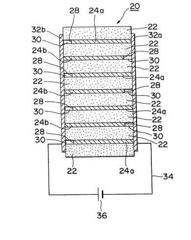
Firstly referring to Fig. 1, laminated ceramic device 20 is
designed as an actuator to be used for a impact printer head or a
X-Y table etc. Said ceramic device 20 comprises a number of
electrostrictive ceramic sheets 22 arranged as so many layers and
also a number of internal electrodes 24 (24a, 24b), each
interposed between two adjacent ceramic sheets 22.
More specifically, said laminated ceramic device 20
comprises a plurality of electrostrictive ceramic sheets 22, a first
and a second groups of filmy internal electrodes 24a, 24b, the
electrodes of said first and second groups being alternately
arranged and interposed one by one between two adjacent
ceramic sheets 22, a first external electrode 32a connected to an
edge of each of the internal electrodes 24a of said first group and
a second external electrode 32b connected to an edge of each of
the internal electrodes 24b of said second group, wherein spaces
~al3s~3
30 are provided between said first external electrode 32a and
each of the internal electrodes 24b of said second group and
between said second external electrode 32b and each of the
internal electrodes 24a of said first group. As a result, the spaces
30 are arranged between two adjacent ceramic sheets 22.
In this embodiment, space 30 is defined by a notch 28
formed at an edge of each of the first and second internal
electrodes 24a, 24b and the opposite surfaces of the ceramic
sheets 22 that sandwich the electrode.
Each of the filmy internal electrode 24 (24a, 24b) is
formed by applying paste of metal onto the surface of a ceramic
sheet 22 as illustrated in Fig. 2. The metal to be used for the
internal electrodes 24 (24a, 24b) may be, for example, platinum,
palladium, silver-palladium alloy or silver. Since the ceramic
sheets 22 are fired after lamination, the paste of metal may
preferably be of a metal that can be baked at the firing
temperature of the ceramic sheets. The paste of metal may
contain powdered zirconia, powdered glass and/or calcined and
powdered ceramic which is chemically equivalent to
electrostrictive ceramic sheets to be used for the purpose of the
present invention in order to improve adhesion between the
ceramic sheets 22 and the corresponding internal electrodes 24
(24a, 24b) after firing.
When an internal electrode 24 (24a or 24b) is formed by
applying paste of metal to the surface of a ceramic sheet 22, a
portion of a peripheral edge thereof is covered with mask to
~313~3
provide a semicircular notch 2~ or a future space 26 which is
devoid of paste of metal as shown in Fig. 2. The notch 28 should
not necessarily be semicircular and may be formed at a corner of
the ceramic sheet 22 as illustrated in Fig. 3.
The thickness of the internal electrodes 24 (24a, 24b) is
preferably between 0.5 ~lm and 20 llm and more preferably
between 1 ~lm and 10 ~lm, although it should not by any means be
limited by these values. Paste of metal may be applied by screen
printing, roller printing or by means of any other appropriate
technique.
The ceramic sheets 22 are made of materials that exhibit
electrostrictive effects after firing and include as principal
ingredients PbTiO3, PbZrO3, and Pb-based composite pezovskite
compound such as Pb(Mgl/3Nb2/3)O3 and Pb(Nil/3Nb2/3)O3. Such
ceramic sheets 22 may be prepared in the following manner prior
to lamination and firing.
~ irstly, if water is used as solvent, a binding agent such as
hydroxyethylcellulose, methylcellulose, polyvinyl-alcohol or a
wax-type slipping reagent and a plasticizer such as glycerol,
polyalkylglycol, solbitonate, tri-ethyleneglycol, petriole or polyole
are added to calcined and powdered ceramic that constitutes the
principal ingredient and then mixed well to form a precursor
mixture for molding. If, on the other hand, an organic solvent
such as ethylalcohol, methylethylketon, benzene or toluene is
used, a binder such as polymethylmethacrylate, polyvinyl-alcohol,
polyvinylbutylal or celluloseacetate and a plasticizer such as
~D139(33
dibutylphthalate, polyethyleneglycol or glycerol to calcined and
powdered ceramic as described above and mixed well to prepare a
precursor mixture for molding.
The precursor mixture is then molded to form a piece of
ceramic having a desired thickness by using a doctor blade
method or by extrusion molding or by means of any other
appropriate technique. After dried, the molded piece is cut to
desired longitudinal and lateral dimensions to become a raw
ceramic sheet 22. The thickness of the raw ceramic sheet 22 is
preferably between 0.02 ~m and 2 llm and more preferably
between 0.05 ~lm and 0.5 ~lm, although it should not by any means
be limited by these values. Thereafter, an internal electrode 24
(24a or 24b) is formed on a surface of the raw ceramic sheet 22
by applying paste of metal.
A raw ceramic sheet 22 according to the invention may
preferably be molded by using water as solvent and by extrusion
molding, although other solvents and molding techniques may be
also feasible as described earlier. If molded in the above
described preferable manner, dried raw ceramic sheets show an
excellent non-adhesiveness to one another with a reduced ratio of
the binder and/or plasticizer contents. Moreover, the so-called
future space 26 formed by a notch 28 on a raw ceramic sheet can
be effectively used for formation of a space 30 after lamination
and firing because the sheet does not adhere to the adjacent
sheets at this area when it is laid between them. It should be
noted that a desirable ceramic sheet 22 having a space 30 may
2~13903
also be adequately prepared by the combination of the use of an
organic solvent and extrusion molding or the combination of the
use of an organic solvent and that of a doctor blade.
The type and amount of the binder and/or plasticizer to
be used and the dring condition under which raw ceramic sheets
22 are formed are so determined that the tensile-shearing-
adhesive strength of each raw ceramic sheet 22 is preferably less
than 10~ and more preferably less than 5% of the tensile strength
of the sheet proper when they are pressed together at
temperature lower than 150C with pressure less than 200
kg/cm2.
When raw ceramic sheets 22 are formed by using water
for solvent and by extrusion molding, the ratio of the binder to be
added to 100 weight portions of calcined powder is preferably
between 1 and 10 weight portions and more preferably between 2
and 5 weight portions, while the ratio of plasticizer to be added to
100 weight portions of calcined powder is also preferably between
1 and 10 weight portions and more preferably between 2 and 5
weight portions.
Then an internal electrode 24 (24a or 24b) with a notch
28 to form a so-called future space 26 is formed on a side of each
of the raw ceramic sheets 22 that have been molded, dried and
cut to a given size. The notch 28 is formed by means of covering a
portion of the surface of the raw ceramic sheet. Thereafter, the
ceramic sheets, each having an internal electrode 24 (24a or 24b),
are put together to form a laminate with their future spaces 26 so
2~139~3
arranged that they alternately face opposite sides of the laminate
as illustrated in Fig. 2. The laminate is then heat pressed,
dewaxed and fired at predetermined temperature. As a result the
internal electrodes 24 (24a, 24b) are firmly bonded to the
corresponding sheets 22. The laminate may be cut to a given size
prior to degreasing or alternatively it may be cut after firing.
Moreover, the so-called future spaces 26 should not necessarily be
so arranged that they alternately face opposite sides of the
laminate. What is important here is that the ceramic sheets are so
arranged that any two adjacent ones have their spaces at different
locations and every other ceramic sheets have their spaces at a
same vertical location. Two groups of spaces of laminate as
illustrated in Fig. 3 may be located at adjacent corners which are
rotationally displaced by 90 from each other.
As a result, the internal electrodes of the first group 24a
and those of the second group 24b are alternately arranged in the
ceramic~ laminate.
When the laminate is fired at high temperature, any two
adjacent ceramic sheets of the laminate come to have an
unbonded area i.e. space 30 that corresponds to the so-called
future space 26 formed by the rounded notch 28 of tne internal
electrode 24 between them.
Then, a first external electrode 32a and a second external
electrode 32b are arranged on the fired laminate and connected
respectively with all the first internal electrodes 24a and all the
second internal electrode 24b to form a laminated ceramic device
2~3~
20. Differently stated, in a laminated ceramic device 20 according
to the invention, the external electrode 32a is connected with a
group of internal electrodes 24a constituted by every other
electrodes of the laminate having their spaces 30 at a same
vertical location of the laminate, while the ex~ernal electrode 32b
is connected with another group of internal electrodes 24b
constitute~ by the rest of the electrodes having their spaces 30 at
another same vertical location of the laminate. The external
electrodes 32a, 32b are preferably made of silver or solder but
not limited thereto. These external electrodes 32a, 32b are
preferably formed by applying paste of silver along two different
lateral sides of the laminate and then baking the applied silver
but the method of forming external electrodes is not necessar;ly
limited to the above described one. It is desirable that the
external electrodes 32a, 32b have a width smaller than that of the
notches 28. If the width of the external electrodes 32a, 32b is
greater than that of the notches 28, the external electrodes 32a,
32b can be short-circuited by way of any of the internal
electrodes 24 (24a, 24b).
While a space 30 is formed at an edge or at a corner of
each of the internal electrode 24 (24a, 24b) of a laminated ceramic
device of the invention in Figs. 1 through 3, such a space may be
formed alternatively between an internal electrode 24 (24a or
24b) and a block 29 as illus~ated in Figs. 4 through 6.
In Fig. 5, a so-called fu~ure space 26 is formed along an
edge of the internal electrode 24 (24a or 24b) formed by applying
13
'~13~
paste of metal to a ceIamic sheet 22 as said future space 26 has a
given width (Q) and carries no paste of metal. Then a layer of an
elongated block 29 is formed along the corresponding edge of the
ceramic sheet 22 and juxtaposed with the internal electrode 24
(24a or 24b) in such a manner that they are separated from each
other by clearance (Q) on the ceramic sheet 22. The block layer
29 may be conveniently formed by applying paste of metal which
is same as that used for formation of internal electrodes 24 (24a,
24b) but alternatively such a block layer 29 may be realized by
using a different material such as a non-conductive material.
When a block layer 29 is formed by applying paste of metal which
is used for internal electrodes 24 (24a, 24b), it may be
conveniently formed in a similar manner as the internal
electrodes. It is desirable that the block layer 29 has a thickness
which is same as that of the corresponding internal electrode 24
(24a or 24b).
While the block layer illustrated in Fig. S has an
elongated shape, it may be differently configured and located as
shown in Fig. 6 for example, where it is located at a corner, of a
ceramic sheet 22 and has a triangular configuration. With such an
arrangement, it will be clear that the internal electrode 24 (24a or
24b) and the block layer 29 are electrically insulated from each
other.
Thereafter, the ceramic sheets, each carrying an internal
electrode 24 (24a or 24b) and a block layer 29, are put together to
form a laminate with their future spaces 26 so arranged that they
14
2~13~3
are found alternately closed to opposite sides of the laminate as
illustrated in Fig. 5. The laminate is then heat pressed, dewaxed
and fired at predetermined temperature. As a result, the internal
electrodes 24 (24a, 24b) are firmly bonded to the corresponding
sheets 22. The laminate may be cut to a given size prior to
degreasing or alternatively it may be cut after firing. Moreover,
the block layers 29 should not necessarily be so arranged that
they are found alternately close to opposite sides of the laminate.
What is important here is that the ceramic sheets are so arranged
that any two adjacent ones have their spaces at different locations
and every other ceramic sheets have their spaces at a same
vertical location. Two groups of spaces of a laminate as illustrated
in Fig. 6 may be located near adjacent corners which are
rotationally displaced by 90 from each other.
Then, a first external electrode 32a and a second external
electrode 32b are arranged along two different lateral sides of the
laminate and connected respectively with all the first internal
electrodes 24a and all the second internal electrode 24b to form a
laminated ceramic device 20. It is recommended that the block
layers 29 are also connected with the respective internal
electrodes 24a, 24b and therefore with the respective external
electrodes 32a, 32b. It is desirable that the external electrodes
32a, 32b have a width smaller than that of the block layers 29. If
the width of the external electrodes 32a, 32b is greater than that
of the block layers 29, the external electrodes 32a, 32b can be
~13~3
short-circuited by way of any of the internal electrodes 24 (24a,
24b).
When a voltage is applied to the external electrodes 32 of
a laminated ceramic device 20 prepared in a manner as described
above by way of a pair of leads 34, an electric field is generated
along the longitudinal direc~ion of the ceramic device 20, which
accordingly deformed in the same direction to operate as an
actuator.
As is apparent from the above description, according to
the invention every other internal electrodes of a laminated
ceramic device can be connected together with ease. Moreover,
the spaces provided within the device effectively prevent
concentration of stress due to uneven distribution of strain caused
by application of an electric field so that the durability of the
device can be improved. Such a laminated ceramic device can be
suitably used for an actuator or other application. Besides, the
concept underlying the present invention can be used for
prevention of any concentration of stress due to uneven
distribution of strain caused by application of an electric field to a
laminated ceramic device which is utilized not for its
electrostrictive effect but for other effects including the
photoelectric effect.
[Examples]
Now the present invention will be described further by
way of examples.
[Example 1]
16
~al3~3
A laminated ceramic device 20 having a configuration as
described below was prepared. A number of ceramic sheets 22
having an electrostrictive effect were so arranged to form a
laminate, in which they alternately carry a first group of filmy
internal electrodes 24a and a second group of filmy internal
electrodes 24b on one by one basis. Then a first external
electrode 32a was formed on a lateral side of the laminate and
connected with each of said first group of internal electrodes 24a
and likewise a second external electrode 32b was formed on
another lateral side of the laminate and connected with each of
said second group of internal electrodes 24b. A space 30 was
provided between said first external electrode 32a and each of
said second internal electrodes 24b and between said second
external electrode 32b and each of said first internal electrodes
24a. In other words, the space 30 was defined by a semic*cular
notch 28 formed at an edge of an internal electrode 24a or 24b
and the opposite surfaces of the two adjacent ceramic sheets that
sandwich the internal electrode.
It should be noted, however, that while the notch 28 has
a semicircular shape in the above example, it may be differently
shaped so long as there is formed an appropriate space defined by
the notch 28 formed at an edge of an internal electrode 24a or
24b, and the opposite surfaces of the two adjacent ceramic sheets
22 that sandwich the internal electrode. Because of the provision
of a notch 28 of an internal electrode, a space 30 is formed
between two adjacent ceramic sheets 22 and consequently the
17
~9~3~
internal electrode 24a or 24b and the juxtaposed external
electrode 32b or 32a are physically and electrically insulated from
each other.
A precursor material of the laminated ceramic device 20
of this example was prepared by adding a prescribed amount of
methylcellulose as binder and also a prescribed amount of glycerol
as plasticizer and water which was used as solvent to an amoun~
of calcined powder of an electrostrictive material containing as
principal ingredients PbTiO3, PbZrO3, Pb(Mgl/3Nb2/3)O3 and mixing
well. Then, a given number of green sheets having a thickness of
120 ~lm were prepared from the precursor material by extrusion
molding and the sheets were dried.
The sheets were then cut to a predetermined size and
paste of silver-palladium was applied to a surface of each of the
sheets by screen printing except for the area for the so-called
semicircular future space 26 as illustrated in Fig. 2 in order to
form an internal electrode 24 (24a or 24b). One hundred green
sheets on which the paste had been applied were put together to
form a laminate and heat pressed. For lamination, the green
sheets were so arranged that the future spaces 26 alternately
faced two adjacent lateral sides of the laminate. The obtained
laminate was dewa~ced at 500C and then fired at 1,100C. The
fired laminate was cut to produce individual devices.
When a section of the fired laminate was observed by
means of a scanning type electronic microscope, each of the
internal electrodes showed a thickness of 2 to 3 ~m and a space
18
hal3~3
with a height of also 2 to 3 ,um was formed at each of the so-called
future spaces 26.
Then a pair of external electrodes 32a, 32b were formed
on each device by applying paste of silver respectively along its
two different lateral sides as illustrated in Fig. 2 which were then
baked so that they were electrically connected with the respective
ends of the corresponding internal electrodes 24 (24a, 24b)
located between two adjacent spaces 30. Then a lead was
soldered to each of the external electrodes and the laminate were
polarized by applying a DC voltage by way of the leads to produce
a laminated ceramic device 20 as illustrated in Fig. 1.
The laminated ceramic device has dimensions of length x
width x height = S mm x S mm x 10 mm. When subjected to a DC
voltage of lOOV, it showed a deformation up to 11 llm. After
sinusoidal voltage pulses having a maximum voltage of 1 OOV with
a frequency of 1 kHz had been continuously applied to the device
for about 100,000,000 times to check the durability of the device,
it did not show any reduction in the value of deformation nor any
functional defects.
[Example 2]
As in the case of Example 1 above, a laminated ceramic
device 20 having a configuration as described below was
prepared. A number of ceramic sheets 22 having an
electrostrictive effect were so arranged to form a laminate, in
which they alternately carry a first group of filmy internal
electrodes 24a and a second group of filmy internal electrodes 24b
19
h~l3~3
on one by one basis. Then a first external electrode 32a was
formed on a lateral side of the laminate and connected with each
of said first group of internal electrodes 24a and likewise a second
external electrode 32b was formed on another lateral side of the
laminate and connected with each of said second group of internal
electrodes 24b.
A block layer 29 was provided between said first
external electrode 32a and each of said second internal electrodes
24b and between said second external electrode 32b and each of
said first internal electrodes 24a so that a space 30 was defined
by the block layer 29, the juxtaposed internal electrode 24a or
24b and the opposite surfaces of the two adjacent ceramic sheets
that sandwich the internal electrode 24a or 24b as well as the
block layer 29.
The first and second external electrodes 32a, 32b were
connected with the respective first and second groups of internal
electrodes 24a, 24b comprising every other internal electrodes
arranged in the laminated ceramic device. Therefore, said first
external electrode 32a and each of said second internal electrodes
24b were physically and electrically insulated from each other by
a space 30 and likewise said second external electrode 32b and
each of said first internal electrodes 24a were physically and
electrically insulated from each other by a space 30.
A precursor material of the laminated ceramic device 20
of this example was prepared by adding a prescribed amount of
methylcellulose as binder and also a prescribed amount of glycerol
,
~13~(33
as plasticizer and water which was used as solvent to an amount
of calcined powder of an electrostrictive material
containing as principal ingredients PbTiO3, PbZrO3,
Pb(Mg1/3Nb2/3)O3 and mixing well. Then, a given number of green
sheets having a thickness of 120 ~m were prepared from the
precursor material by extrusion molding and the sheets were
dried.
The sheets were then cut to a predetermined size and
paste of silver-palladium was applied to a surface of each of the
sheets by screen printing except for the area for the so-called
future space 26 having width (Q) of 0.5 mm as illustrated in Fig. S
in order to form an internal electrode 24 (24a or 24b) and a
corresponding block layer 29 separated from each other by the
so-called future space 26. One hundred green sheets on which the
paste had been applied were put together to form a laminate and
heat pressed. For lamination, the green sheets were so arranged
that the block layers 29 alternately faced two adjacent lateral
sides of the laminate. The obtained laminate was dewaxed at
500C and then fired at 1,100C. The fired laminate was cut to
produce individual devices.
When a section of the fired laminate was observed by
means of a scanning type electronic microscope, each of the
internal elec~rodes 24 (24a, 24b) and the corresponding block
layer 29 showed a thickness of 2 to 3 llm and a space 30 with a
height of also 2 to 3 ,um was formed at each of the so-called future
2~33~
spaces 26 between the internal electrode 24 (24a or 24b) and the
block layer 29.
Then a pair of external electrodes 32a, 32b were formed
on each device by applying paste of silver respectively along its
two different lateral sides as illustrated in Fig. S which were then
baked so that they were electrically connected with the respective
ends of the corresponding internal electrodes 24 (24a, 24b)
located between two adjacent blocks 29. Then a lead was soldered
to each of the external electrodes and the laminate were polarized
by applying a DC voltage by way of the leads to produce a
laminated ceramic device 20 as illustrated in Fig. 4.
The laminated ceramic device has dimensions of length x
width x height = S mm x S mm x 10 mm. When subjected to a DC
voltage of lOOV, it showed a deformation up to 10 llm. After
sinusoidal voltage pulse having a maximum voltage of lOOV with
a frequency of 1 kHz had been successively applied to the device
for approximately 100,000,000 times to check the durability of
the device, it did not show any reduction in the value of
deformation nor any functional defects.
[Comparison Example]
For the purpose of comparison, a laminated ceramic
device of a conventional type as illustrated in Fig. 7 was prepared
and subjected to the same durability test, in which voltage pulses
were successively applied to the specimen for approximately
10,000 times. As a result of the test, the specimen was
destructed .
22
~a~3~3
Therefore, a laminated ceramic device according to the
present invention can effectively prevent concentration of stress
due to uneven distribution of strain caused by application of an
electric field because of the spaces provided at the edges of the
internal electrodes and consequently has a remarkably improved
durability as compared with a conventional laminated ceramic
device illustrated in Fig. 7.
However, a laminated ceramic device according to the
present invention can be prepared without requiring provision of
insulation layers as that of a conventional laminated ceramic
device illustrated in Fig. 8. Therefore, a laminated ceramic device
according to the invention is free from any malfunctions due to
defective insulation layers. Such laminated ceramic devices can
be manufactured with a high yield by a relatively s;mple manner.
When the external electrode is formed by applying paste
of metal, it is preferable that a laminated ceramic device according
to the invention has block layers in the point of preventing the
paste from blowing into the areas of internal electrodes.
23