Note: Descriptions are shown in the official language in which they were submitted.
CA 02013930 1999-04-O1
- RCA 85,533
_1_
BEAM CURRENT LIMITER WITH
BRIGHTNESS CONTROL THRESHOLD EXTENSION
This invention relates generally to electron beam current
limiting in kinescopes of television receivers, video monitors and the like.
More particularly, the invention relates to the field of electron beam current
limiting in conjunction with image contrast and brightness control over an
extended range.
This application is related to copending and commonly owned
Canadian Patent application S.N. 2,013,344 filed March 29, 1990, and entitled
BRIGHTNESS MODULATOR FOR CLOSED LOOOP COMPENSATION OF
BLACK LEVEL.
In most television receivers the display device is a cathode ray
tube whose high voltage power is provided from the horizontal deflection
system
by rectifying the pulses generated during successive horizontal scan retraces.
Power drawn from the supply is a function of picture content, customer setting
of
black level (or brightness); video gain (or contrast or picture) controls;
and, the
effect of whatever form of forms of automatic video gain and/or automatic
black
level control may be implemented. Power is drawn during active picture time
and replenished during horizontal retrace time. The likelihood of high beam
current being produced increases in the presence of video signals
representative
of bright images containing predominantly white information, manual contrast
or
brightness control settings at a maximum position, or a combination of these
factors.
Excessive beam current may cause a receiver to produce a
degraded image and may cause a receiver to be damaged. Excessive beam
current may adversely effect performance of receiver's deflection system, may
cause electron beam spot defocusing and may result in picture blooming.
Accordingly, receivers are usually provided with an automatic beam limiter
circuit. Such a circuit senses beam current, and automatically reduces
contrast
or brightness levels, or both, when beam current increases beyond a
predetermined value.
2 - FiCA 85,533
r r n y n G'
Typically, a horizontal deflection system includes a
flyback transformer. A voltage proportional to the beam current
is developed across a resistor connected from the lower end of a
secondary winding of the flyback transformer to a source of
reference potential. The voltage at the terminal of the resistor
not coupled to the reference potential is actively compared
against another reference in a control circuit. When a desired
maximum beam current is reached, action is taken to reduce video
gain, or contrast, so as to limit the current. Further protection
against excessive beam current often is provided by an additional
circuit designed to reduce black level, or brightness, after video
gain has been reduced by some predetermined amount. The
additional circuit can be similar in structure and coupled in
parallel to the gain control, using the same beam sense voltage
for the different comparator reference, so that action to reduce
black level starts at a higher beam current than action to reduce
video gain. Alternatively, the additional circuit can be coupled
serially to the gain control, and be designed to begin operation
when the output of the gain control reaches a predetermined
degree of video gain reduction.
Automatic brightness limiting may present problems
even for levels of beam current which are not necessarily
excessive. A beam current limiter should function without
unnecessarily increasing a viewer's perception of changes in
image content due to operation of the beam limiter. ta;enerally
speaking, a viewer can often perceive changes in the background
illumination of an image produced by changes in image brightness
more readily than image contrast. Moreover, reducing black level,
or brightness, under normal picture conditions is undesirable
because it results in cutting off low light detail in the scene,
assuming black level was set correctly initially. Accordingly,
beam current limiting in safe ranges of beam
current levels is preferably effected by limiting contrast.
However, automatic beam current limiting circuits are generally
susceptible to noise and frequently operate to prematurely reduce
1
_ 3 _ RCA 85,533
brightness, and thereby image quality, before beam current levels
become excessive.
Various automatic beam current limiter systems are
known which operate in conjunction with contrast and brightness
control circuits of a television receiver and the like. Many
systems provide for progressive control of contrast and
brightness over predetermined ranges of beam current, but none
provide for extending the useful control range of contrast
adjustment before the limiting of the brightness, or black level,
perceptibly degrades image quality. Sequential and progressive
beam limiter systems are described in the following U.S. Patents:
4,126,884 - Shanley, 11; 4,253,110 - Harwood, et al.; 4,253,121
Avery; and, 4,137,552 - Serafini.
it is an aspect of this invention to provide control of
contrast and brightness levels responsive to beam current levels
in a first, safe and extended range of beam current levels.
It is a further aspect of this invention to reduce
brightness levels responsive to values of beam current levels in a
second range of levels with an extended threshold of operation.
It is another aspect of this invention to delay onset of
brightness limiter control, but thereafter, to effect rapid
reduction of beam current.
!t is yet another aspect of this invention to control
contrast over an extended range of beam current values responsive
to a control signal, and to control brightness limiting in a further
range of beam current values, responsive to a processed variation
of the same cantrol signal.
it is yet another aspect of this invention to control
brightness limiting only during horizontal trace times and to
prevent control of brightness limiting during horizontal retrace
times.
A video control circuit in accordance with the
foregoing aspects of this invention may comprise a gain
controllable video amplifier for a video signal, the amplified
video signal generating a picture having contrast and brightness
characteristics which both vary directly with the gain of the
_ q. _ RCA &x,533
f ~ ki !~. e~ l'~ cb
amplifier, and a brightness control circuit for varying the
brightness of the amplified video signal without affecting the
contrast. A beam current sensing circuit is used to develop a
beam current control signal related, for example, to an average
picture intensity level. An automatic contrast control circuit and
an automatic contrast limiter are coupled to the amplifier. The
automatic contrast control circuit is continuously responsive to
the video signal, and in particular, to peaks in the video signal
which will cause brief peaks in the beam current which do not
significantly affect the average value of the beam current. In this
respect, the video signal is an indirect measure of peaks in the
beam current. The contrast limiter is continuously responsive to
the beam current control signal, which does not generally reflect
peak conditions, but average values. The contrast control and
contrast iimiter may be thought of as being responsive to
different aspects of beam current values, indirectly and directly,
in a first and extended range of beam current operating values.
Each of the contrast control and contrast limiter develops a
component of a contrast control signal for continuously varying
the gain of the video amplifier to adjust the contrast and control
beam current. A brightness modulator is coupled to the brightness
control circuit and is responsive to the video gain control signal
for developing a brightness control signal, for example, for
continuously adjusting the brightness of the video signal
inversely with the contrast, thereby increasing the brightness of
both white and dark portions of the picture when the entire
picture has a sufficiently large average picture intensity level to
cause the contrast control circuit to effect reduction of the
contrast and the brightness.
in order to maximia~e the effective range over which
contrast control and brightness modulation are effective, without
at the same time preventing timely operation of the brightness
limiter, the beam current control signal is processed to remove
certain characteristic noise signals, for example by filtering or
gating, which do not significantly alter the average level of
sensed beam current, but which engender premature operation of
- 5 - RGA 35,533
lr~_we~~~.
the brightness iimiter. The brightness limiter is therefore
operated responsive to a processed beam current control signal, to
preclude undesirable operation of the brightness limiter when the
beam current is in the first and extended range of operating
values.
It is yet another aspect of this invention to provide a
beam limiter in a video control circuit which provides for an
extended range of contrast control and brightness modulation, and
which is compatible with manual contrast arnd brightness
controls.
These and other aspects of the invention may be better
understood with reference to the drawings, in which:
FIGURE 1 is a block diagram of a video control circuit
in accordance with this invention;
FIGURE 2 is a circuit schematic for the beam current
limiting circuitry shown in FIGURE 1, wherein the signal
processor for the beam current control signal is a filter;
FIGURE 3 is a graph illustrating beam sense voltage
waveforms for selected values of beam current;
FIGURE 4 is a graph illustrating variation of the
contrast level control voltage and the beam current overload
control voltage as a function of beam current;
FIGURE 5 is a graph illustrating variation of the
brightness control voltage produced by the brightness madulator
as a function of the contrast control voltage;
FIGURE 6 is a schematic for a beam current limiting
circuit wherein the signal processor is a gate control; and,
FIGURE 7 is an alternative circuit to that shown in
FIGURE 6.
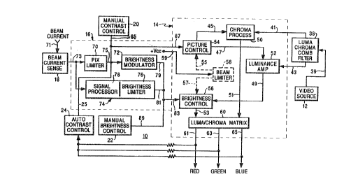
A video control circuit is shown in block diagram form
in FIGURE 1 and generally designated by reference numeral 10.
The video control circuit 1 Q comprises a video source 1 ~, a
lumalchroma processing circuit 14, a beam current limiter circuit
16, a beam current sensing circuit 1$, a manual contrast control
circuit 2Q, an automatic contrast control circuit 2~ and a manual
brightness control circuit 22.
- 6 - RCA 85,533
.,
6~~.~.~~:'~
The output of the video source 12 on line 39 is an input
to a fuma/chroma comb filter 38. The output of the comb filter on
line 41 is chrominance information and the output of the comb
filter on line 43 is luminance information. The outputs of the
comb filter 38 are inputs to the luma/chroma processing circuit
14. Such circuits as the luma/chroma process>ing circuit 14 may
be embodied as integrated circuits. Such a luma/chroma
processing chip is available as RCA part no. 1421882-1, Thomson
Consumer Electronics, Indianapolis, Indiana. (7nly those portions
of such a luma/chroma chip as are pertinent to this invention are
illustrated.
The chrominance output of the comb filter 38 is an
input to a chrome processing circuit 50. The luminance output of
the comb filter 38 is an input to a luminance amplifier 52. A
picture control circuit 54 controls video gain of the luminance and
chrominance channels, and has outputs on lines 45 and 47, which
are inputs respectively to the chrominance processing circuit 50
and the luminance amplifier 52. The output of the luminance
amplifier 52 is an input to a brightness control circuit 56.
Brightness control circuit 56 raises and towers the brightness
level, also termed black level. The output of the brightness
control circuit 56 on line 53 and the output of the chrome
processing circuit 50 on line 51 are inputs to a luma/chroma
matrix 60. The outputs of the luma/chroma matrix 60 on lines 61,
63 and 65 provides output for the red, green and blue video
signals, respectively. Each of the outputs on lines 61, 63 and 65
is passed through a resistor, after which the outputs are summed
as an input to a conventional automatic contrast control circuit
24. This enables beam current limiting to be effected responsive
to video peak intensity, as well as average picture intensity. This
can prevent localized defocusing and blistering of the shadow
mask.
A video signal is generally clamped to a DC level at 0
IRE (back porch of the composite video signal), whereas the black
level in NTSC signals is nominally adjusted to be approximately
7.5 IRE. lNhite level is nominally 100 IRE. Accordingly, an
- 7 - RCA 85,533
~.~ ,,
increase in video gain causes the displayed black level to move
"brighter" as video gain is increased and causes the displayed
black level to move "darker" as video gain is decreased. Vllhen
beam current limiting circuits also respond to increases in beam
current levels by reducing brightness, that is lowering the black
level, the effect can be pronounced.
The picture control circuit has an input on line 87. The
brightness control circuit 56 has an input on line 83. For purposes
of definition, and in accordance with operation of the integrated
circuit chip identified above, an increase in a voltage level
applied to input line 87 of picture control 54 will increase the
gain of the video amplifier. The increase in video gain will
therefore increase the contrast level and increase, or raise, the
brightness level. A reduction in the voltage on line 87 will cause
a reduction in video gain, which will result in a reduction of the
contrast level and a reduction of the brightness level. Similarly,
an increase of voltage on input line 83 to brightness control 56
will be effective to raise the brightness level of the video signal,
and a reduction of voltage on line 83 will be effective to lower
the brightness level. P-iowever, variations of the voltage level on
input line 83 to brightness control circuit 56 will not affect the
video gain, and accordingly, will not change the contrast level.
In the particular embodiment which is disclosed in the
drawings, which utilizes a luma/chroma chip as identified above,
a beam limiter circuit 58 is also provided. Beam limiter circuit
58 is shown by a block drawn in phantom, because it is not
utilized in the invention. In order to render the beam iimiter 58
ineffective, its input on line 59 is permanently coupled to a
substantially uniform and raised voltage level +Vcc. This
indicates, albeit falsely, that beam current is very low. Vvhen the
input to beam limner circuit 58 is thus tied high, its outputs on
lines 55 and 57, to the picture control 54 and brightness control
56 respectively, are unchanging and of no effect. In this manner it
is possible to disable the integrated beam limiter circuit 58, and
substitute the beam limiter circuit 16 to which an aspect of this
invention is directed.
- 8 - RBA 85,533
The specific operation of the luma/chroma comb
filter, the chroma processing circuit, the luminance amplifier and
the luma/chroma matrix are known, and accordingly, are neither
shown nor explained in detail. The operation of the beam lirniter
circuit 58, which is bypassed, was in accordance with a prior art
scheme, which adjusted contrast and brightness in the same
direction in a first range of beam current levels, and in a higher
range of beam current levels than in the first range, adjusted
brightness level. It is the less than optimum operation of such a
beam limiter circuit, which prompted the development of the
beam iimiter circuit taught herein.
Electron beam current on line 71 is monitored by beam
current sensing circuit 18. Beam current sensing circuit 18
develops a beam current control voltage on line 73, which is an
input to a contrast, or "pix", limiter circuit 70 and a beam current
control 74. Beam current control 74 comprises a brightness
limiter 78 and a signal processor 78. Signal processor 78 may
take different forms, for example, a filter as shown in FIGURE 2
or a gate control as shown in FIGURES 5 and 7. in either case, the
signal processor 78 is a means for removing at least certain
characteristic noise from the input to the brightness iimiter 76.
In accordance with the circuit schematic shown in FIGURE ~, the
beam current control signal is a voltage signal, which is at a
maximum when beam current is at minimum, and is at a minimum
when beam current level is at maximum.
The pix limiter circuit 70 is an automatic contrast
limiting circuit, which develops one component of a contrast, or
pix, control voltage on output line 75 responsive to dynamic
variations of beam current related to average picture intensity.
Another component of the pix control voltage is the output of the
automatic contrast control 24 on line 25, responsive to dynamic
variations of beam current related to peak picture intensity. A
third component of the pix control voltage is the output of the
manual contrast control 20 on line 85. The pix control voltage on
line 75 is an input to a brightness modulator circuit 72 and the
input line 87 of picture control circuit 54. A net increase of the
_ g _ RCA 55,533
pix control voltage, due to any or al! ofi its components, causes the
picture control circuit 54 to increase the video gain, which
increases the contrast level and raises the brightness level. A net
decrease in the pix control voltage causes the picture control
circuit 54 to reduce the video gain, decreasing contrast and
lowering the brightness level. The pix control voltage varies as a
function of beam current responsive to the pix limiter 70 as
shown in FIGURE 4. In order to highlight operation of the pix
limiter, the effect of the brightness modulator is ignored in
FIGURE 4. The values correspond to operation of the specific
circuit shown in FIGURE 2. At lower values of beam current than
shown in FIGURE 4, the pix control voltage varies conventionally,
for the most part, responsive to the auto contrast control 24.
The brightness modulator circuit 72 provides an output
control voltage on line 79 which varies inversely with the pix
control voltage, as illustrated in FIGURE 5. The values correspond
to operation of the specific circuit shown in FIGURE 2. YVhen the
pix control voltage increases, the voltage of the brightness
contral signal on line 79 decreases, which causes the brightness
control circuit 56 to lower the brightness level. Conversely, when
the pix control voltage falls, the brightness control voltage rises,
causing the brightness control circuit 56 to raise the brightness
level. Increasing the video gain increases the contrast level, and
at the same time, raises the brightness level. Conversely,
reducing the video gain reduces the contrast level and lowers the
brightness level. The brightness control signal is therefore
effective to raise the brightness level when the contrast level is
reduced and to lower the brightness level when the contrast level
is increased. The brightness modulator therefore counteracts the
particularly undesirable reduction of the brightness level when
the contrast is decreased responsive to auto contrast control or
beam current iimiter operation.
The brightness modulator 72 is effective in a first
range of beam current operating values, corresponding generally
to safe operating conditions. However, there are certain
circumstances wherein perceived image quality is less important
-1 0 - RCA 85,533
~I i ~~ ~~
than the dangers of excessive beam current levels. Accor~i~'gP~,
the brightness limiter circuit 76 is effective in a second range of
beam current operating values, corresponding generally to unsafe
operating conditions, that is, where neither the auto contrast
control 24 nor the pix limiter circuit 70 is effective to prevent
unsafe beam current levels. Under these circumstances, the
brightness limiter circuit 78 develops a beam current overload
control voltage signal on line 81, which is also coupled to input
line 83 of brightness control circuit 56. The beam current
overload control signal is also shown in FIGURE 4, as a function of
beam current. In order to highlight operation of the brightness ,
limiter, the effect of the brightness modulator is ignored in
FIGURE 4. It will be appreciated that, at a certain threshold value
of beam current, the pix limiter 70 will have reached its ful6
range of adjustment, so that no
further changes on the input to the picture control circuit or from
the brightness modulator circuit will take place. The beam
current overload control signal is thereafter effective in the
second range to lower the brightness level to prevent unsafe beam
current levels.
In order to prevent the brightness limiter circuit 76
from generating the beam current overload control signal when
the auto contrast control or the pix limiter should still be capable
of controlling the beam current by controlling the video gain, the
beam current control signal is passed through the signal processor
78 to remove AC components therefrom, for example noise spikes
resulting from retrace pulses. This helps assure that the
brightness limiter circuit 76 will become effective only when the
full and extended range of compensation provided by the pix
control voltage has been exhausted. The dash line curve in FIGURE
4 shows the premature effect of the brightness limiter without
the signal processor.
Most television receivers provide manually adjustable
means whereby viewers may alter the contrast and brightness
settings. As noted, the output of the manual contrast control
circuit 20 is also coupled to 'the input of the' brightness modulator
-1 1 - RCA 85,533
< ~~~~
72, which will be effective to reduce the brightness level
responsive to a manual increase of contrast. As in the automatic
beam limiter circuit 16, the manual brightness control 22 will
raise and lower the brightness level without affecting video gain
and contrast level. However, the voltage level on output line 89
will be a component of the input to the brightness control circuit
56, and an unduly high manually adjusted brightness level will
result in a reduced effective range of the pix control and
brightness modulator, and will result in more frequent operation
of the brightness limiter circuit.
A circuit schematic for a suitable beam limiter circuit
16 in accordance with this invention is shown in FICIJRE 2. An
electron beam current flows through line 71 and into winding W of
flyback transformer T1. A beam current sensing circuit 18
includes resistors R1 and R2, the junction of which corresponds to
line 73, on which a beam current control voltage Vs is developed.
Ream current control voltage Vs varies inversely with beam
current. Diode D1 is connected between output line 73 and a
supply voltage, for example +11.2 volts. This Limits the maximum
value of voltage Vs to approximately +12 volts.
The pix limiter circuit 70 comprises transistors Q1
and Q2, the emitters of which are coupled to one another through
resistor R9. The base of resistor Q1 is biased by a voltage divider
network comprising resistors R5, R6 and R7. For the component
values shown, the base of transistor Q1, which is coupled to the
junction of resistors R5 and R6, is biased at a voltage level of
approximately +4 volts.
The auto contrast control circuit 24 may be embodied
as a variety of specific circuits, for example as taught in IJ.S.
patent No. 4,599,643, incorporated herein by reference. One such
embodiment comprises a transistor. The transistor has a base
electrode coupled to the summed video outputs, a collector
electrode coupled to the outputs of the pix iimiter and the manual
contrast control and an emitter electrode coupled by a resistive
voltage divider network to a biasing voltage. An increase of video
drive (amplitude) will effect reduction of the pix control voltage.
-1 2 - RCA 85,533
,~ . ,~ -'
~~~W~A~
The brightness iimiter circuit 76 comprises
transistors C~5 and Q6, the emitters of which are coupled to one
another through resistor R8. The base of transistor Q5 is also
biased by the voltage divider network comprising resistors R5, R6
and R7. For the component values shown, the base of transistor
Q5, which is coupled to the junction of resistor's R6 and R7, is at
approximately +2.7 volts. Signal processor 78, in the form of a
filter 76, is coupled to the base of transistor t~6 and comprises
resistor R4 and capacitor C2.
The brightness modulator circuit 72 comprises
transistors Q3 and Q4. The base of transistor Q4 is biased by the
voltage divider network comprising resistors R11 and
R12, and is coupled to the junction thereof. The voPtage at the
emitter of transistor Q3 follows the voltage on the base thereof,
and is essentially the pix control voltage. The collector of
transistor Q1 is the output of the pix control circuit 70, and
corresponds to output line 75. Qutput line 75 is an input to the
picture control circuit 54 and, through resistor R10, is also an
input to the brightness modulator circuit 72 at the base of
transistor Q3.
The collector of transistor C~5 is the output of the
brightness limiter circuit 76, and corresponds to output line 81.
This is coupled to the collector of transistor Q4, which is the
output of the brightness modulator 72, and corresponds to output
line 79. Diode D2 does not form part of the brightness limiter or
brightness modulator, but prevents conduction of transistors Q4
and ~5 when the customer, or manual, brightness control is set
abnormally low. Resistor R5 of the voltage divider network, the
collector of transistor Q3 and one terminal of resistor R13 are
coupled to the supply voltage +11.2 volts. Resistor R13 and
resistor R14 form a voltage divider network for biasing the
emitter electrode of transistor Q4, which is coupled to the
junction thereof. When transistor C~3 is not conducting, the
emitter electrode of transistor of Q4 is at a voltage level of
approximately +.85 volts.
-1 3 - RCA 85,533
The manual contrast control circuit will result in a
voltage level on input line 75 to the picture control circuit, which
voltage will also appear at the collector of transistor Q1, which
is the output of the pix control circuit 70. Assuming, for example,
that beam current is at a minimum and that the voltage Vs is at a
maximum, a nominal factory setting of the manual contrast
control, for the component values illustrated, will generate a
voltage level of approximately +7.8 volts on line 75 at the input to
the picture control circuit and on the collector of transistor C~1.
Transistor Q3 is biased in such a fashion that it will conduct
responsive to pix control voltages in excess of approximately +5
volts. Accordingly, even in the absence of any beam current
limiting resulting from the level of voltage Vs, transistor Q3 will
conduct, which in turn will cause transistor Q~ to conduct, which
will set the output of the brightness modulator on line 83 to
approximately +6.1 volts. This corresponds to the maximum
brightness control voltage shown in FIGURE 4, wherein the effect
of the brightness modulation is ignored.
Voltage Vs will fall as beam current rises. The auto
contrast control will be effective, and predominate, before enough
beam current flows to turn on transistor Q2. When voltage Vs
falls low enough to forward bias the base emitter junction of
transistor Q2, which will be approximately two diode drops below
the +4 volts bias voltage on the base of transistor Q1, transistor
Q1 will begin to conduct. As transistor Q1 begins to conduct, the
pix control voltage on output line 75 will be pulled down. As the
pix control voltage falls, the video gain will be reduced, and the
contrast level will be reduced. Reduction of the video gain will
also Power the brightness level, as explained above. However, as
the pix control voltage falls, the voltage at the base of transistor
Q3 will fall, which will reduce the conduction of transistor Q3.
t-ess conduction of transistor Q3 will result in less conduction of
transistor Q4, which will cause the voltage level at the collector
of Q4 on output line 79 to increase. Accordingly, the brightness
control signal will increase, and raise the brightness level to
compensate for the reduction in video gain.
- ~ 4 ~ RDA 55,533
The value of voltage Vs at which the pix control
circuit becomes effective will depend upon the values of resistors
R5, R6 and R7, which set the bias voltage at the base of transistor
t~l, which in turn sets the bias voltage for the emitter of
transistor f~2. As voltage Vs falls further, with increasing beam
current, the pix control voltage at the collector of transistor Q1
will continue to fall and the brightness control voltage at the
collector of transistor of Q4 will continue to increase.
Ideally, the brightness limiter circuit will become
effective when the voltage Vs becomes small enough, but not
before. More particularly, the voltage divider formed by resistors
R5, R6 and R7 sets the bias voltage at the base of transistor Q5,
which in turn sets the bias voltage at the emitter of transistor
Q6. When voltage Vs falls approximately two diode drops below
+2.7 volts, transistor C~6 will begin to conduct, which causes
conduction of transistor Q5. As transistor C~5 begins to conduct,
the brightness control signal at the output of the brightness
modulator, namely the collector of transistor Q4, will be pulled
down. This will cause the brightness control to lower the
brightness level to reduce beam current. The further voltage Vs
falls, the lower the brightness level will be pulled.
The auto contrast control 24 and the contrast limiter
70 may be thought of as operable in different parts of a first
range of beam current values, with the brightness limner being
operable in a second range of beam current values beyond the first
range. Alternatively, the auto contrast control may be thought of
as operable in a first range of beam current values, the contrast
limiter as operable in a second range of beam current values and
the brightness limiter as operable in a third range of beam current
values beyond the first and second ranges.
FIGURE 3 illustrates typical beam sense voltages for
several different levels of beam current. When beam current is 0
milliamps, as shown by waveform 3A, protective diode D1
conducts and prevents the beam sense voltage from rising above
approximately +12 volts. As beam current increases, current is
diverted from the diode D1 until, at a current on the order of
-1 5 - RCA 85,533
~~.~ ~j,~ ~a .
E' ~, e~ e.S ~?
approximately 850 microamps, the diode ceases to conduct. ~~en
beam current flows, the beam sense voltage has one value during
active picture time and a significantly lowo~r value for a few
microseconds during horizontal scan retrace.
The beam sense voltage at a current of approximately
1.16 milliamps (ma) is shown in waveform 3B.
At currents exceeding this value, conduction occurs in transistors
Q1 and Q2 (initially during the negative spike) and the consequent
reduction in voltage at the collector of transistor Q1 acts to
reduce video gain. The onset of pix limiter action to reduce video
gain would be more abrupt if the spikes were not present, but the
less abrupt reduction in video gain that occurs with them
normally is acceptable. Brightness limiter action to reduce black
level, however, should not begin until significant reduction in
video gain has taken place, and then should act rapidly.
The beam sense voltage at a current of approximately
1.22 mifliamps is shown in waveform 3D. At currents exceeding
this value, undesirable conduction would occur in transistors Q5
and Q6 during the negative spikes, with consequent action by the
brightness limiter to reduce black level if the beam sense voltage
were applied directly to the base of transistor Q4, instead of
being filtered by the action of resistor R4 and capacitor C2. Such
premature action to reduce black level is typical of prior art
circuits. Waveforms 3D and 3E show the beam sense voltage at
currents of approximately 1.38 milliamps and 1.47 milliamps
respectively. For waveform 3F, the baseline voltage is already
bePow the threshold, and the effect of the spikes is not a
signifianct concern. When the negative spikes are prevented from
causing conduction in transistors C~5 and Q6, the beam limiter
structure formed by transistors Q1 and Q2 can conduct heavily and
act to reduce video gain substantially, before any action is taken
to reduce black level. As shown in FI~IJRE 4, brightness, or black
level, control reduction begins almost as soon as picture, or video
gain, control reduction without the filter, whereas with the filter
brightness control reduction is delayed until significant picture
control reduction has occurred.
-1 8 - RCA 85,533
,r,,s~. ~,~~~
In the context of the circuit shown in FIGURE 2, ~'~ ~~ ~~ ~ t~~~ n~
biasing transistor Q5 only moderately below L~1 should cause the
brightness limiter to operate when the pix control circuit has
reduced video gain as much as is possible and
voltage 1/s falls further as beam current increases further.
However, the negative pulses (spikes) during retrace cause the
brightness limiter to conduct at lower beam .current levels than
desired, unless transistor Q5 is biased much below the transistor
of C~1. However, it is not practical to bias transistor Q5 much
below the level of transistor Q1, as the brightness limiter would
not be sufficiently effective. The signal processor 78, for
example, the filter formed by resistor R4 and capacitor C2,
substantially eliminates the AC component (negative spikes) from
the signal Vs. The effective control range is therefore
significantly extended before beam current limiting by brightness
reduction takes piece.
The effect of the negative spikes can also be inhibited
by controlling propagation of the beam sense control voltage
signal to the brightness limiter andlor the pix limiter, for
example, by a suitable gate circuit. FIGURE 6 illustrates the
circuit shown in FIGURE 2, as modified to include a signal
processor in the form of a gate circuit 77. The gate circuit 77
comprises a transistor Q7, resistors R~ 6 and R17 and diode ~D3.
Diode D3 has a cathode coupled to the emitter electrode of
transistor Q5 and an anode coupled to one terminal of resistor R16
and to the emitter electrode of transistor Q7. The collector
electrode of transistor Q7 is coupled to the supply voltage +11:2
volts. The base electrode of transistor t~7 is connected to one
terminal of resistor R17 and forms an input to the gate circuit.
The other ends of resistors R16 and Ri7 are coupled to ground.
The circuit shown in FIGURE 6 operates substantially identically
to that shown in FIGURE 2, except for the influence of gate circuit
77. The filter network comprising resistor R~ and capacitor C2
has been omitted, so that the same beam sense signal is an input
to the pix limiter circuit 70 at the base electrode of transistor C~2
-1 7 - RCA 85,533
=~5 ~,j
l~ ~r~c.~
and to the brightness limiter 76 at the base electrode of
transistor Q6.
Transistor G7 is normally turned off, but is turned on
during harizontal retrace by flyback pulses applied to its base
electrode. When the transistor Q7 is turned on, diode D3 becomes
forward biased and raises the voltage level at the emitter of
transistor C~5 above the voltage levee at the base electrode of the
transistor Q5, turning transistor Q5 off. This prevents transistor
Q5 from conducting responsive to conduction of transistor C~6
under the influence of the negative spikes in the beam sense
voltage. The brightness limiter 76 is free to operate as described
previously during trace. The auto contrast control 24 is not
affected by gate circuit 77, and so continues to operate during
retrace as well as during trace.
The use of a different gate circuit is shown in FIGURE
7. The circuit shown in FIGURE 7 dififers from those shown in
FIGURES 1, 2 and 5, in so far as a brightness modulator has not
been included. The beam sense voltage developed at the junction
of resistors R1 and R2 and diode D1 is applied to the base
electrode of transistor Q8, which inverts the beam sense voltage.
The inverted beam sense voltage developed at the collector
electrode of transistor Q8 is applied as an input to the base
electrodes of transistors Q9 and Q10. Transistors C~9 and Q10 are
shown as NPN transistors. Transistor Q9 is a pix limner which
generates a component of the pix control voltage as an output on
its collector electrode. The other components are generated by
the manual contrast control and the auto contrast control.
Transistor Q10 generates a brightness control voltage as an
output on its collector electrode. Resistors R18 and R19 may be
on the order of a few kilohms, and may be identical in value,
although they need not b8 identical. Resistors R20, R21 and R22
may be selected to enable operation at thresholds which
correspond to the circuits shown in FIGURES 2 and 5, although this
need not necessarily be the case. For the values shown, transistor
C~8 begins to conduct when the beam sense voltage applied to its
_ 1 8 - RCA 85,533
~.' ljt~s5t
base electrode falls more than approximately VBE of transis'~'or~ ~~~'J '~ ~
below +11.3 volts. As transistor t~8 begins to conduct, the voltage
at its collector electrode begins to rise. When the voltage at the
collector electrode of transistor Q8 rises above approximately
VB~ of transistor a9, transistor Q9 begins to conduct. When
transistor Q9 begins to conduct, the pix control voltage begins to
fall, which effects a reduction in video gain. The emitter of
transistor Q10 is so biased that when the voltage at the collector
electrode of transistor Q8 increases to approximately 1.3 volts in
excess of VB~ of transistor Q10, transistor 0110 begins to conduct
and effect a reduction of the black level. Gate transistor t~'I1 is
normally turned off, but is turned on during horizontal retrace, for
example by flyback pulses applied to its base electrode or by
pulses which are in timed relationship with the flyback pulses.
When transistor C~11 is turned on, it pulls down the voltage signal
applied to the bases of transistors Q9 and t~10, assuring that
transistors C~9 and Q10 will be turned off during retrace, and
effectively preventing propagation of the beam sense voltage
signal when the characteristic negative spikes appear in the beam
sense voltage signal. The auto contrast control 24 is not affected
by operation of transistor Q11.
The auto contrast control and the pix limiter circuit
control beam current levels over different parts of a first and
relatively wide range of values during which time the brightness
modulator, if present, compensates for all undesirable changes in
the brightness level due to changes in the video gain responsive to
the pix control voltage. As beam current levels reach an extended
threshold of unsafe values, in a second range of values, the
brightness limiter becomes effective to lower the brightness
level markedly to prevent damage and picture degradation from
beam current overload. A signal processor for the beam current
sense voltage signs! prevents premature operation of the
brightness limiter.