Note: Descriptions are shown in the official language in which they were submitted.
1 This invention relates to analog-to-digital converters
2 and more particularly relates to non~linear analog-to-digital
3 converters for providing indications of unknown input values in
4 any desired scale such as a luminance scale or a combination of
a luminance scale for high values and a linear scale for Low
6 values.
8 Data processing qystems operate on digital signals.
9 However, the inputs to the data processing systems are generally
analogO For example, video signals may be continuously measured
11 in a sy,stem for digital video re~ording. These measurements
12 have to be converted to a digital form before they can be
13 introduced to the digital data recording system for storage by
14 such system. Linear analog-to-digital converters have been in
~se for a considerable number o~ years to convert such video
16 signals into a digital form~ Because the dynamic range, or
17 ratio of largest to smallest detectable signal, is approximately
18 1000 to 1, a linear analog-to-digital converter for video
19 applications would be required to obtain a resolution of the
video siqnals into approximately 1000 parts.
21
22 There are two (2) important parameters in considering
23 the performance of analog-to-digital converters. These are ~1)
24 the speed of the conversion and (2~ the resolution or accuracy
with which the analo~ data is converted to a digital form. The
26 converters now in use have been successful in accomplishing only
27 one (1) o these two (2) parameters.
28
29 In one type of converter, a flash converter, a
plurality of comparators are employed to operate on a
31
~4~
l simultaneous - or parallel - basis. In order to provide an
2 accuracy in the conversion, a large n-~ber of comparators have
3 to be used. For example, when a conversion has to be made to
4 ten ~10) binary bits, one thousand and twenty four (1024)
comparators have to be used. As will be appreciated, this
6 causes the converter to be large, complex, expensive and
7 difficult to produ~eO
9 In another type of converter, successive
approximations are made to convert the analog value to the
ll corresponding digi~al ~alue. In each approximation, ~he value
12 of progressive bits of reduced binary significance is
13 determined. This type of converter is relatively simple and can
l4 be quite accura~e, particularly if the number of successive
approximations is relatively larqe. However, this type of
16 converter is slow. Furthermore, the time required to obtain a
17 conversion lncreases as the accuracy of the conversion is
8 increased.
19
One possible solution to the problem of digitizing
21 vi~eo signals is to use a converter which has logarithmic or
22 nlog" characteristics. In this type o~ converter, the
23 resolution is mada inversely proportional to the signal level.
24 This results in a constant fractional resolution over the range
of conversion. The log conversion characteristic is not the
26 most desira~le non-linear conversion characteristic for video
27 signals. At the low end of the dynamic range, the log
28 characteristic has steps which are too fine by comparison to the
29 luminance response of the human eye. Conversely, at the high
end of the dynamic range, the steps are too coarse~
31
32
~ 4~
Logarithmic converters have traditionally been
2 constructed by using components such as silicon diodes to
3 generate the required input to-output transfer characteristic.
4 The silicon diode is useful for this purpose because it has a
logarithmic current to voltage charac:teristic. Unfortunately,
6 the conversion characteristic of a silicon diode has some
temperature instabilities that cause significant errors, on the
8 order of several millivolts, in the digiti2ation o voltages.
9 Since the signals at the low end of the dynamic range of a video
signal are typically just a few millivolts, the errors ln the
~1 CQnVerSion characteristics of the diode produce sizable
12 distortions.
13
14 This invention provides an analog~to-digital converter
which overcomes the difficulties discussed above. The converter
16 of this invention has any desired non-linear conversion
17 characteristic, such as the luminance characteristic of the
18 human eye. The converter is fast, simple and inexpensive. In
19 one embodiment, ~he converter includes a pair of resisti~e film
dividers whlch, when interconnected as taught by this invention,
21 become relatively insensitive to linear gradients in the
22 thickness ~or resistivity) of ~he film in any direction. The
23 ilm dividers can simply and precisely match the l~inance
24 characteristic at low signal levels where the luminance
characteristic becomes linear.
26
27 In one embodiment of the invention J a ~Eirst film is
28 disposed on an integrated circuit chip in a first direction to
29 provide progressiYely increasing resistance values at
progressive positions along the Eilm. The film has uniformly
31
32
1 spaced taps. First and second reference voltages may be
2 respectively applied to the first and second ends of the film.
4 A second film may be disposed on the chip in a
direction opposite to the ~irst dir~ction at a po~ition
6 displaced in any direction from the first film. The second film
7 may have a construction corresponding to that o the first film.
8 The first and second reference voltages may be respectively
9 applied to the first and second ends of the second film.
Particular taps on the first film may be connected to taps in
11 corresponding positions on the second Eilm.
12
13 A plurality of diferential comparators are provided,
14 each with a signal input and a reference input. Each ComparatQr
lS reference input is connected to an individual one of the taps on
16 the ~irst ilm, hut not necessarily to successive taps. The
17 re~erence input connections to the taps on the first film may
~8 have a non-linear (e.g. lu~inance) spacing in the ~irst
19 direction to provide a non-linear voltage (e.g. luminance)
relationship between such taps. An input voltage is applied to
21 the signal input of all of the comparators. Binary signals
22 representative of the input voltage are produced by the
23 comparator in which the input voltage is substantially equal to
24 the reference input voltage.
26 In the drawings:
27
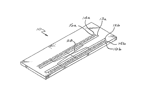
28 Figure 1 is a schematic perspective view of an
29 integrated circuit chip incorporating one embodiment of the
31
l invention and including first and second reference films
2 disposed on the chip;
4 ~igure 2 is El schematic circuit diagram, partly in
5 block form, of one embodiment o the invention for indlcating
6 the value o~ an unknown input value in a non-linear scale;
~ Figure 3 is an enlarged block diagram illustrating the
9 connection of certain elements of the embodiment o~ Figure 2 to
lO the elements on the integrated circuit chip of Figure 1; and
11
12 Figure 4 is a simplified illustration of another
13 embodiment o~ the invention for providing a plurality of
14 non-linear reference voltages for high reference va:Lues and for
providing a plurality of linear reference voltages ~for low
16 reference values.
17
18 In the embodiment of the invention shown :in Figure 1,
l9 an integrated circuit chip generally indicated at 10 is
provided. The chip may have a suitable length such as
21 approximately one fourth of an inch (1/4~ and a suitable width
22 such as approximately one tenth of an inch (1~10~ hin film
23 strips 12a and 12b made from a material with electrically
24 resistive properties is formed in a conventional manner on the
chip 10. The films 12a and 12b may be illustratively be formed
26 from a material such as polysilicon having a thickness of
27 approximately one half ~1/2) micron.
28
29 ~he film 12a is preferably disposed in El first
direction such as a vertical direction in Figures 1-3.
31
l Preferably the thin film 12a extends, at substantially equally
2 spaced displacements in the Eirst direction, in a second
3 direction coordinate with the first directionO At these
4 positions? the film 12a preferably defines pads 14a. Each of
the pads 14a is preferably provided with a rectangular
6 configuration. ~ach of the pads 14a is completely filled with
q the resistive material. Taps 16a may be provided within the
8 pads 1~a at substantially identical positions within the
g different pads.
rhe film 12b may be also formed on the chip 10 wi~h
12 characteristics substantially iden~ical to the film 12. The
13 ilm 12b may be displaced from the film 12a, pre~erably in the
14 second direction, such as the horiæontal direction. The film
12b may be disposed in an opposite direction to the film 12a so
16 that the first end of the film 1~b is opposite to the first end
17 of the film 12a. The film 12b may be provided with pads 14b
18 corresponding to the pads 14a. Taps 16b may be provided within
l9 the pads 14~ at substantially the same positions as the
positions of the taps 16a within ~he pads 12a.
21
22 . An energizing potential such as from a voltage source
23 24 is applied to the first ends of the thin film 12a and the
24 thin film 12b. A reference potential such as a ground 2~
~Figure 2) may be applied to the s~cond ends of the film 12a and
26 the film 12b. In this way, each of the films 1~a and 12b
27 operates as a voltage divider in producing, in each of the
28 descending taps 16a and in each of the ascending taps 16b, a
29 voltage of progressively increasing magnitude. Xnstead of
connecting 4he second ends of the thin films 12a and 12b to a
31
32
l reference potential such as ground, these ends may be connected
2 to a reerence potential having a negative value.
4 Although each o the thin films 12a and 1 2b is for~ed
~ by sophisticated manufacturing techniques~ differential
6 linearity errors may occur in the resistance value prvvided by
7 each of the thin films at progressive positions in the films.
8 For example t these errors may occur as a result of progressi~e
9 changes in the thickness of the films at ~uccessive positions
along the films or they may occur as a result of progressive
ll changes.in the composition o~ the thi~ film material at
12 successive positio~s along the thin films. For example,
13 differential linearity errors as high as one half of one percent
14 (0.5%) may occur in a chip having a length and a width of
approximately one half of an inch (O~5"). Although $hese
l6 deviations are not great, they may affect the accuracy of the
17 conversion of an analog value to a digital value, particularly
18 when it is desired that the conversion by quite precise.
1~
A~ will be seen, the differential linearity errors
21 discussed in the previous paragraph generally occur in a
22 particular direction. Thus, if positive errors occur in an
23 upward direction at progressive positions in the thin film 12a,
24 negative errors of corresponding magnitude will occur at such
progressive positions in a downward direction in the thin film
26 12b. Because the films 12a and 12b extend in opposite
27 directions, the voltage decreases at progressive positions
28 upwardly in the thin film 12a in Figure 2 but d~creases with
29 progressive positions downwardly in ~he thin film 12b.
31
32
l Thus, by connecting the thin films 12a and 1~b ~t
~ progressive, but isolated, positions as by leads 28, an average
3 is obtained between the di~ferential voltages between the
4 successive taps 16a and 16b on the films to compensate for any
~ errors resul~ing from differential non-linearities in either or
6 both of the f ilm~ ~ ~he connections are made to correspondi~
7 taps on the thin films 12a and 12b. Each of the leads 28
8 extends between an individual one of the taps 16a on the thin
g film 12a and a corresponding one of the taps 16b on the film
12b. Such i~dividual taps 1~a ~n the thin film 12a and such
ll corresponding taps 16b on the ilm 12b are those which would
12 provide equal voltages i there were no di~erential
13 non-linearitie~ in the thin films~ Only a limited number, such
14 as sixtee~ ( 16 ) of connections has to be proviaed between the
thin films 12a and 12b by the leads 28. Because of this, only a
16 limited number of the taps 16a need be connected on the thin
17 film 12a.
18
l9 Leads 30 extend from pre-selected ones of the taps 16b
in the thin film 12b to first input terminals of comparators 32
21 which may be constructed in a conventional manner. ~he taps 16b
22 may be pre-selected to provide the input voltages to successive
23 ones of the comparators 32 with a particular scale. For
24 example, the individual taps 16b connected to the comparators 32
may be pre-selected to provide the input voltages to the
26 comparators 3~ with a non-linear scale, such as a logarithmic
27 scale, as shown in the embodiment of Figure 3. In a
28 l ogarithmic scale, the distances between successive ones of the
29 taps 16b connected to the comparator 32 increase on a
logarithmic basis.
31
32
1 An input voltage is introduced to second input
2 terminals of the comparator~ 32 a~ from an electrical terminal
3 34. Each of the comparator~ 32 operates in a conventional
4 manner to compare the magnitude of the input voltage on the
5 terminal 34 with the voltage introduced to the comparator from
6 the thin film 12b~ Each of the comparators 32 has two output
7 terminals. ~ne of the output terminals from each individual
8 compartor 32 and the other output terminal from the next one o
9 the comparators are connected to input terminals o~ an
associated "nand" network 36. Bach of the "nand" networks 36
ll compare~ the polarity o~ the ~ignals on its two input terminals
72 and inaicates the results o~ the comparison on its outpu~
13 terminal.
14
I~ ~wo (2) suca~ssive comparators 32 in the plurality,
16 the results of the comparison will be opposite. In other words,
l~ one such comparator will indicate a greater magnitude of the
18 input voltage than the voltage rom the thin film 12b and the
l9 other ¢omparator will ~ndicate a lesser magnitude of the input
voltage than the voltage from the thin film 12b. The position
21 of these two ~uccessive comparators 32 in the plurality provides
22 an indication of the magnitude of the input voltage on the
23 terminal 34. The comparison ~etween the voltages on successive
24 pairs of comparators is provided by the "nand" gates 36 each o~
which provides an output signal of a particular polarity only
26 when the voltages introduced to the terminals in the "nandQ gate
27 have the polarity of a logical "one. The first :Logical one i~
28 provided at the upper or ~assertions~ output of the lower o the
29 two comparators. The ~econd logical "one~ is pro1~ided at the
31
~2
l lower or ~negations~ output of the upper of the two
2 comparators.
4 The converter described above can provide binary
indications of the input voltage on the terminal 34 wi~h great
6 accuracy. For example if the thin film 12b is considered to
7 provide a voltage divider with four thousand and ninety six
8 (4096~ taps 16b along a linear distance of approximately 0.496
9 in~hes, the center-to-center spacing bekween successive ones of
the taps 16b may be approxima-tely one tenth oE one mil (0.1 mil)
ll or appr~oxi~ately two and one half microns (~.5~ ).
12
13 A~sume that the integrated ciruit chip 10 i3
14 formulated by eight tenths of a micron (0.8 ~) technoloqy.
Under such circumstances, there would be ample spacing between
16 successive tap3 16b to route metal leads 28, if necessary, from
17 successive taps 16b to successive ones of the comparators 32 at
18 the end of the thin film 12b near the ground 26. At the low end
19 of the vol~age divider defined by the thin film 12b, successive
ones of the taps 16b may have to be connected to successive ones
21 o~ the comparators 32 to provide a linear conversion.
22
23 Conne~tions may then be made wi~h any required
24 spacing between successive ones of the taps 1~b to a linear
array of the comparators 32 positioned on the chip 10 adjacent
26 to the thin film 12b. For examples if the comparator pitch
27 should be one mil (1 mil) or twenty five microns (25~ as many
28 as four hundred and ninety six (496) comparators 32 may be
29 disposed on the chip 10 along the length of the thin fil~ 12b,
Under such circumstances~ the converter described above may
31
l provide a conversion with a dynamic range of over four thousand
2 ~4,000) to one (1).
4 As can be seen, a non-linear conversion, such as a
logarithmic conversion, between analog and digital values can be
: 6 provided throughout the full range of the thin film 12b. For
7 example, this may occur when the conversion is provided for the
8 imag~s on an x-ray film. However, under other circumstances, it
g may be desirable to provide a non~linear conversion, such as a
luminance conversion, throughout most of the range of the thin
ll film 12b but to provide a linear conversion a~ the low end o~
12 thi~ range. For ex~mple, although the human eye provides a
13 luminance conversion of visual images r a linear conversion at
14 the low end of the intensity range may be desirable for video
film images. Such a conversion may be desirable since the human
16 eye is not able to provide a non-linear conversion of video
17 images at low light intensities. Under such circumstances, the
l~ taps 16b connected to the comparators 32 may have a linear
19 dlsplacement relative to one another in this low range. This i~
~ndicated a~ 40 in Figure 4.
21
22 . A8 will be seen from the above discussion, the
23 converter constituting thîs invention is able to convert an
24 analog value to a digital value in any desired non-linear scale,
2~ or combinat~on of non linear scales or combination of non-linear
26 and linear scales, in a highly accurate and simple manner. The
2~ converter of ~his invention is ~ble to provide this accuracy in
28 conversion ~y the formulation of an integrated circuit chip in a
29 manner well known in the art. ~he converter provides this
accuracy in conversion by the use of a single th.in resistive
31
32
~fl~
1 film or a compensating pair of thin resistive films to provide
2 resultant reslstance values which compensate or diferential
3 non-linearities in each of the thin films. The formulation of
4 resistance value~ compensating for the differential
non-linearities ~n each of a pair of thin films on an integrated
6 circuit chip and the cross connections between the resistances
7 at a relatively few positions of corresponding value on the
8 resistances believed to be inventive in themselves.
Although this invention has been disclosecl an~
11 ill~str~t~d with reference to particular embodiments, the
12 principles involved are susceptible for use in numerous o~her
13 embodiments wh~ch w~ll be apparent to persons s~illed in the
14 art. The invention is, therefore, to be limited only as
indicated by the scope of the appended claims.
16
17
18
19
ZO
~1
22
23
~4
26
27
28
29
31
32