Note: Descriptions are shown in the official language in which they were submitted.
1
INTEGRATED CIRCUIT
FIELD OF THE INVENTION
The present invention relates to an improvement
of a depletion type field effect transistor (MOSFET) and
in particular to an enhancement/depletion type inverter
consisting of the FET stated above and an enhancement
type FET and a semiconductor integrated circuit, in
which these FETs or inverters are integrated on a
substrate.
BACKGROUND OF THE INVENTION
Increase in the speed and increase in the degree
of integration of an integrated circuit using MOSFETs
have been advanced, accompanied by the decrease in the
size.
For example, contrarily to the fact that in a
1M D-RAM the smallest channel length is about l.3um, it
is possible t o realize an MOSFET having a channel length
of about O.lum. Although the switching speed of a
semiconductor logic circuit is increased together with
the decrease in the size, it is said that the working
speed thereof is generally lower than that of a logic
integrated circuit using bipolar transistors. However
the switching speed of the MOSFET increases due to the
increase in the mobility and the saturation speed, if
the working temperature is lowered from the room
temperature (300K) to the liquid nitrogen temperature
(77K). Further it is known that the RC time constant in
the wiring is decreased by the decrease in the wiring
2
resistance so that the working speed of the integrated
circuit using MOSFETs can be as high as the working
speed of the integrated circuit using bipolar
transistors.
It is known also that, since electric power
consumption per gate for the MOSFET integrated circuit
is smaller than that for the bipolar transistor
integrated circuit, the degree of integration per chip
' thereof is greater than that of the bipolar transistor
integrated circuit. Thus it is possible to realize a
high speed high integration LSI by driving the MOSFET
integrated circuit at the liquid nitrogen temperature.
Even if a bipolar transistor is driven at the
liquid nitrogen temperature, the switching speed thereof
is not increased because of the freeze out in the base
layer.
Heretofore the source voltage for the MOSFET was
determined at 5V, in order to hold the interchangeability
with TTL. However, if the source voltage is kept at 5V,
for an MOSFET having a channel length smaller than l4am,
the electric field strength within the element is
increased. Thus it has become more and more difficult
to secure the normal operation and the reliability of
the MOSFET because of hot carrier deterioration and
drain break down. Consequently, for the MOSFET having a
channel length smaller than lum, the source voltage for
the integrated circuit cannot help being decreased. For
example, in the case of a channel length of 0.5um, it ~is
estimated to be about 3.3V and in the case of a channel
length of O.lum, it is estimated to be about 1 to 1.5V.
.
3
Therefore, as a high speed high density integrated
circuit provided both with a speed as high as that of
the integrated circuit using bipolar transistors and
with a high integration density of the MOSFET integrated
circuit, the operation of fine MOSFETs having a channel
length smaller than lum at the liquid nitrogen temperature
(77K) is expected.
heretofore it was said that e.g. a Yosephson
logic circuit working at the liquid helium temperature
(4.2K) can realize a high speed logic integrated circuit.
however, since a Yosephson logic element utilizing the
superconduction phenomenon works only in the neighborhood
of 4.2K and it cannot work at the room temperature, the
operation thereof cannot be checked at the room tempera-
tune. For example, in the case of constructing a large
scale computer, it is not possible to exchange rapidly
defective chips or boards and in the case of constructing
a system therefor, tremendous work and time are necessary.
Therefore it is practically impossible to construct any
large scale system. Consequently in a system, by which
it is tried to obtain a high performance by a low
temperature operation, it is necessary that the device
or the system can be driven both at the room temperature
and at the low temperature, although the working speed
2'5 is low at the room temperature.
A prior art MOSFET integrated circuit driven at
liquid nitrogen temperature is constructed by a comple-
mentary type (CMOS) logic circuit composed of CMOS
circuits, because the threshold voltage thereof does not
vary significantly between the room temperature and 77K.
4
However, since a logic circuit of enhancement/depletion
structure (hereinbelow called E/0 structure) can be
constructed only by n channel MOSFETs, the fabrication
process therefor is easier than that for the CMOS logic
circuit, for which it is required to integrate p channel
MOSFETs and n channel MOSFETs on a same substrate.
Further, since an HAND or NOR circuit having n inputs is
constructed by 2n MOSFETs by the GMOS structure, contrarily
- to the fact that it is constructed by (n+1) MOSFETs by
the E/D structure, in the case where a same logic circuit
is constructed, the E/D structure has an advantage that
it can be constructed by, less MOSFETs than the CMOS
structure.
Consequently, if a logic circuit of E/D structure
can be constructed in a so small size that the channel
length thereof is smaller than 0.5um and driven stably
both at the room temperature and at the liquid nitrogen
temperature, a ultra-high speed ultra-high density
integrated circuit provided with both the high speed of
the bipolar transistor and the high density integration
of the MOSFET can be realized by a relatively simple
- process, as described previously.
However an MOSFET logic circuit of prior art E/D
structure had following problems and could not exhibit
the characteristics described above.
Figure 7(A) shows an example of the prior art
inverter circuit of E/D structure, in which reference
numeral 1 is an input terminal; 2 is an output terminal;
3 is a source terminal; 4 is a depletion type n channel
MOSFET; 5 is an enhancement type n channel MOSFET; and 6
4
5
is the ground. Since a logic integrated circuit or a
memory integrated circuit is constructed by a modifica-
tion of an inverter, it is constructed by 2 MOSFETs,
which are an enhancement type n channel MOSFET 5 and a
depletion type n channel MOSFET 4. The inverter as
described above is the basic unit of the integrated
circuit. Since, in general, in Si the mobility of
electrons is greater than the mobility of holes, n
channel MOSFETs, by which a high speed operation is
possible, are used. In the following explanation the
case where n channel MOSFETs are used is taken as an
example. Figure 7(B) shows an example of output
characteristics of the inverter.
In the operation of the inverter circuit indicated
in Figure 7(A), when the voltage in the input voltage
Vin applied to the input terminal 1 is sufficiently
lower than VINV' a voltage, which is approximately equal
to the source voltage VDD applied to the source terminal
3, is produced at the output terminal 2. When a voltage,
which is approximately equal to the source voltage VDD'
is applied as the input voltage Vi~~, the output voltage
Vout has a level almost equal to zero. In practice the
level is not at zero, but a slight voltage VLOW is
produced. Usually the voltage VLOW is about 1/10 of the
source voltage VDD'
Concerning the characteristics SE and SD of the
enhancement type n channel MOSFET and the depletion type
n channel MOSFET, as indicated in Figure 8, the gate
voltage, by which the drain current. ID begins to flow,
when the gate voltage V~ is applied, i.e. the threshold
6
voltage Vth is positive (VthE) for the enhancement type
and negative (VthD) for the depletion type.
In order to realize the inverter operation as
indicated in Figure 7(B), the threshold voltages VthE
and VthD of the enhancement type and the depletion type
MOSFET constituting the inverter is designed so as to be
about 0.2 VDD and -0.6 VDD, respectively. Figure 9 is
a cross sectional view of an example of the MOSFET of
E/D structure indicated in Figure 7(A), which is an
MOSFET of E/D structure fabricated by the known LOCOS
isolation method.
In the figure, reference numeral 7 is a p conduc-
tivity type Si substrate; 8 is a field oxide film; 9 is
a p~ doped region (channel stopper); 10 is an n+ doped
region (acting as the source region S of the enhancement
type MOSFET>; 11 is another n+ doped region (acting as
the drain region D of the enhancement type MOSFET and
the source region S of the depletion type MOSFET formed
in a same region); 12 is still another n+ doped region
(acting as the drain region D of the depletion type
MOSFET); l3 is a gate insulating film for the enhancement
type MOSFET; 14 is a gate electrode for the enhancement
type MOSFET; 15 is a channel doped region of the enhance-
ment type MOSFET doped with impurities of same conductivity
as the p conductivity type Si; 16 and 17 are a gate
oxide film and a gate electrode for the depletion type
MOSFET, respectively; 18 and 18' are channel doped
regions of the depletion type MOSFET doped with impurities
of conductivity type opposite to the p conductivity type
Si; 19 is a PSG film (insulating film); 20 is an electrode
4
7
connected electrically with the gate electrode 16 for
the depletion type MOSFET; 21 is an AX, metal wiring
(ground line); 22 is an AQ metal wiring (source line);
23 represents the channel length of the enhancement type
MOSFET; and 24 represents the channel length of the
depletion type MOSFET.
The gate electrodes 14 and 14 are made of n+
polycrystalline silicon. Ions of impurities such as B,
etc, having the same conductivity type as the p conduc-
tivity type Si substrate 7 are implanted in the channel
doped region 15 just below the gate oxide film 13 for
the enhancement type MOSFET to adjust the threshold
voltage VthE of the enhancement type MOSFET so as to be
about 0.2 VDD with respect to the source voltage VDD' p
or As ions, which are impurities having the conductivity
type opposite to the p conductivity type Si substrate 7
are implanted in the channel doped region 18 just below
the gate oxide film 16 for the depletion type MOSFET to
adjust the threshold voltage VthD of the depletion type
MOSFET so as to be about -0.6 VDD with respect to the
source voltage VDD.
The electrode 20 connected electrically with the
gate electrode 17 for the depletion type MOSFET is
extended in a plane perpendicular to the sheet. The
electrode 20 is made of the same material as the gate
electrode for the depletion type MOSFET, i.e. n~
polycrystalline Si. The source of the depletion type
MOSFET and the drain of the enhancement type MOSFET are
connected with the n~ region 11 through the electrode
connected electrically with the gate electrode i7 for
s
the depletion type MOSFET. The electrode 20 serves as
the output terminal 2 of the inverter circuit indicated
in Figure 7(A).
Since the enhancement type MOSFET forms an n
type inverted layer in the surface portion of the Si
substrate by bending electrically the forbidden band in
the surface portion of the p conductivity type Si
substrate by the voltage applied to the gate electrode,
both at the room temperature and at the liquid nitrogen
temperature it performs the enhancement type operation,
i.e. the threshold voltage VthE remains positive.
However, although the depletion type MOSFET, in which P
or As ions, which are impurities having the conductivity
type opposite to the p conductivity type Si substrate 7,
are implanted to form intentionally the n type channel
18' just below the gate oxide film 16 performs the
depletion operation at the room temperature, at the
liquid nitrogen temperature, since As or P implanted as
opposite conductivity type impurities is frozen out and
not ionized, in the case where no gate voltage is applied,
no n channel layer is formed just below the gate oxide
film 16 and therefore it does not perform the depletion
operation. That is, the MOSFET, which can perform the
depletion operation owing to the implanted impurities of
opposite conductivity type, performs the enhancement
operation at the liquid nitrogen temperature.
- Consequently, there was a problem that although
the prior art inverter of E/A structure using depletion
type MOSFETs including the channel portion 18' doped'
with the impurities of opposite conductivity type
~~r~~~y~,~
9
performs the normal operation at the room temperature,
i~t cannot perform the normal operation at the liquid
nitrogen temperature.
The MOSFET logic circuit of E/D structure is
characterized in that the fabrication process is easier
and the number of MOSFETs at constructing a same logic
circuit is smaller with respect to the logic circuit of
CMOS structure.
The working speed of the logic circuits remains
almost equal both for the E/D structure and for the CMOS
structure and it is possible also therefor to increase
the working speed by the operation at the liquid nitrogen
temperature. However, as described previously, the
inverter of E/D structure using depletion MOSFETs, in
which the channel is doped with impurities of conduc-
tivity type opposite to the conductivity type of the
used semiconductor substrate, has a drawback that it
cannot perform the depletion operation at the low
temperature, because the impurities are frozen out at
that time.
OBJECT OF THE INVENTION
The object of the present invention is to provide
an MOSFET capable o~ performing the depletion operation
without doping the channel portion with impurities of
conductivity type opposite to the conductivity type of
the used semiconductor substrate and a method for
constructing an inverter of E/D structure using it.
SUMP9ARX OF THE INVENTION
An MOSFET according to the present invention is
characterized in that the surface portion of a semicon-
to
doctor body just below an insulating film, on which the
gate electrode is disposed, is not doped with impurities
of conductivity type opposite to the conductivity type
of the semiconductor substrate, and in the case where
the conductivity type of the semiconductor substrate is
p, the work function of the gate electrode is smaller
than that of the substrate and in the case where the
conductivity type of the substrate is n, the work
function of the gate electrode is greater than that of
the substrate.
If an MOSFET is constructed as described above,
the forbidden band for the surface portion of the
substrate is bent towards the negative side by the
difference in the work function in an energy band
diagrarn using the electron energy. Therefore, although
the surface portion is not doped with impurities of
conductivity type opposite to that of the substrate, an
n type inverted layer is formed in the surface portion
of the substrate. Since the work function do almost not
vary, depending on the temperature, the n type inverted
layer is formed in the surface portion of the substrate
both at the room temperature and at the liquid nitrogen
temperature.
Consequently the D10SFET constructed as described
above can realize the depletion operation both at the
room temperature and at the low temperature.
Further, when an E/D inverter is constructed,
using a depletion type MOSFET constructed as described
above and a prior art enhancement tyge MOSFET, it can
perform the inverter operation both on the room tempera-
11
Lure and at the liquid nitrogen temperature. In particular
at the low temperature it is possible to realize a logic
circuit having a high switching speed owing to the
increase in the mobility or the saturation speed.
BRIEF DESCRIPTION OF THE DRAWINGS
Figure 1 is a cross sectional view of an embodi-
ment of the depletion type MOSFET, in which the channel
portion is not doped with impurities of conductivity type
opposite to the conductivity type of the substrate
according to the present invention;
Figure 2 is a graph showing an example of measure-
ments of the high frequency C-V curve for the depletion
type MOSFET according to the present invention;
Figure 3 is a diagram showing the relation
between the impurity concentration in the substrate, for
which the threshold voltage is negati~~e, and the thickness
of the gate oxide film in the embodiment indicated in
Figure l;
Figure 4 is a cross sectional view of the n
channel MOSFET inverter of E/D structure, for the depletion
type MOSFET of which the channel is not doped with
' impurities of conductivity type opposite to the conduc-
tivity type of the substrate;
Figure 5(A) is a circuit diagram of the E/D
inverter according to the present invention;
Figure 5 (B) is a graph showing an example of
in/out characteristics of the E/D inverter indicated in
Figure 5(A) for a channel length of 0.5um;
Figure 6(A) is a circuit diagram of the E/D
inverter according to the present invention;
~~~L~ '~~' ~'~
12
Figure 6(B) is a graph showing an example of
in/output characteristics of the E/D inverter indicated
in Figure f,(A) for a channel length of 0.lum;
Figure 7(A) is a circuit diagram of a prior art
MOSFET inverter circuit of E/D structure;
Figure 7(B) is a graph showing an example of
in/output characteristics of the prior art MOSFET inverter
of E/D structure indicated in Figure 7(A):
' Figure 8 is a graph showing an example of drain
current (ID) vs. gate voltage (V~) characteristics of a
prior art depletion type and a prior art enhancement type
n channel MOSFET; and
Figure 9 is a cross sectional view of a prior
art n channel MOSFET inverter of E/D structure, for the
depletion type MOSFET of which the channel is doped with
impurities of conductivity type opposite to the conduc-
tivity type of the substrate.
DETAILED DESCRIPTION
Hereinbelow the present invention will be explained,
referring to the embodiments indicated in the drawings.
Figure 1 is a cross sectional view of an embodiment
of the depletion type MOSFET, in which the channel
portion is not doped with impurities of conductivity
type opposite to the conductivity type of the substrate
according to the present invention.
In Figure 1, the same reference numerals as
those used for Figure 7 (A) represent identical or
similar parts, and 25 is an n~ doped region (the source
region S of the depletion type MOSFET). The surface
channel portion 18' of the Si substrate 17 just below
13
the insulating film 16 for the gate electrode 17 is not
dbped with impurities of conductivity type (n type)
opposite to the conductivity type of the substrate 7.
This portion 18' may be doped with impurities of same
conductivity type (p type) as the substrate 7. Further
the gate electrode 17 is made of a material having a
work function, which is smaller than the work function
of the p conductivity type Si substrate 7. The Si
' substrate 7 may be of n conductivity type. In this
case, the portion 18' described above is not doped with
impurities of p conductivity type and the gate electrode
17 is made of a material. having a work function greater
than the work function of the substrate 7. Also in this
case, the portion corresponding to the portion 18'
stated above may be doped with impurities of same
conductivity type as the n conductivity type substrate.
The basic structure is identical to that of an
enhancement type n channel MOSFET fabricated by the
LOCOS isolation method and the fabrication process
therefor is identical to the well known n channel MOSFET
process. The element isolation may be effected by any
isolation method other than LOCOS isolation method, if
elements can be isolated thereby.
If the gate electrode were made of n~ type
polycrystalline silicon, it would be a usual enhancement
type n channel MOSFET.
One of the features of the present invention is
that the gate electrode is not made of n+ type polycry-
stalline silicon, but a material having a small work
function is used therefor. It i:s required~for the
~~_~a~~~
14
material for the gate electrode to have a work function
smaller than about 4eV and it is desirable that the work
function is as small as possible. Simple metals such as
Mg, Sc, Y, Ba, La, Ce, Pr, Nd, Er, ete. and compounds
such as LaB6, etc. may be used therefor. Among them it
is desirable to use La, Mg or LaB6, because they are
matched with the conventional silicon process and have a
high melting point and a high workability. In particular,
- LaB6, has a work function of about 2.5eV and it belongs
to the group having the smallest work function among the
materials described above. Further it has a melting
point higher than 800°C and it is chemically stable. In
addition, since a thin film of LaB6 can be formed easily
by the well known electron beam evaporation method and
the crystallographical orientation can be controlled by
selecting the evaporation condition,.LaB6 is one of the
most desirable materials.
In the embodiment according to the present
invention Mg, La and LaB6 were used for the gate elec-
trode 17. However other materials may be used therefor,
if they have a work function smaller than about 4eV,
' they are chemically stable, and they, have a melting
point higher than 800°C.
When a material having a work function smaller
than 3.5eV is used for the gate electrode, the forbidden
band in the surface portion just below the gate oxide
film is bent by the difference in the work function
between the material and the p conductivity type Si and
the surface portion is inverted to the n conductivity
type. That is, it is possible to form the n type
h
15
channel layer in the surface portion just below the gate
oxide film without forming intentionally the n type
region by implanting ions of P or As, which are
impurities of conductivity type opposite to the conduc-
tivity type of the substrate, by the ion implantation in
the channel portion 18' of the p conductivity type Si
substrate just below the gate oxide film 16.
Figure 2 is a graph showing an example of measure-
ments of the high frequency C-V curve of an MIS diode
between the gate electrode 17 and the p conductivity
type Si substrate 7 for a frequency of about lMHz at a
temperature of 300K, e.g. when the impurity concentration
in the p conductivity type Si substrate is 1x1016cm 3;
the gate oxide film is about 20nm thick; and the LaB6
gate electrode is about 500nm thick. The threshold
voltage, at which the surface portion of the p conduc-
tivity type Si substrate of this MIS diode was inverted,
was about -1.6V. The C-V curve obtained at the liquid
nitrogen temperature was about equal to that obtained at
the room temperature and the threshold voltage was also
equal to that obtained at the room temperature, i.e.
about -1.6V.
In the drain current (ID)-gate voltage (V~)
characteristics of the enhancement type MOSFET having a
channel length of about lum. VthD was about -1.6V both
at the room temperature and at 77K. Further; in the
case where the dimensions described previously and a
gate electrode made of Mg were used, the threshold
voltage was about -0.9V both at the room temperature and
at 77K.
h
16
As explained in the above embodiment, it is
possible to turn the threshold voltage to a negative
value by using a material having a small work function
for the gate electrode without doping intentionally the
portion of the p conductivity type 5i substrate just
below the gate oxide film with impurities (P, As, etc»)
of conductivity type opposite to the conductivity type
of the substrate.
' The condition, under which the threshold voltage
is turned to a negative value, depended principally on
the resistivity of the p conductivity type Si substrate
and the thickness of the.gate oxide film and not on the
thickness of the gate electrode. In the case where LaB6
was used, the threshold voltage depended slightly also
on the orientation of the crystallographical surface of
the LaB6 film and varied by about 0.3V, depending on the
orientation.
For example, in the case~where the impurity
concentration in the p conductivity type Si substrate is
about 1x101~cm 3 (resistivity of about 1.55~~cm), when
LaB6 is used for the gate electrode and the thickness of
the gate oxide film is smaller than about 40nm, the
threshold voltage is negative. Figure 3 shows the
relation between the impurity concentration NA in the p
conductivity type Si substrate, whose threshold voltage
is turned to a negative value by using LaB6 and Mg for
the gate electrode, and the thickness H of the gate
oxide film. For example, when the thickness of the gate
oxide film and the impurity concentration are in a region
below the respective line (hatched region) in Figure 3,
6
17
the threshold voltage is negative. The MIS diode, for
which the characteristics are indicated in Figures 2 and
3, is a sample, in which the interfacial level density
is e.g. 1 to 2x1010cm 3. In the case of the n channel
MOSFET, if the interfacial level density is high, since
the threshold voltage increases in the negative direction,
an interfacial level density higher than 2x1010cm-3 may
be used also as well.
- For MIS diodes having different interfacial
level densities characteristics indicated in Figures 2
and 3 are different. In any way, in order to turn the
threshold value to a negative value, it was necessary to
use a material having a small work function for the gate
electrode.
As described above, although the threshold
voltage is negative for the n channel MOSFET, for the
inverter of E/D structure the magnitude o~ the threshold
voltage is a problem. For the inverter of E/D structure,
the threshold voltage VINV of the inverter is defined as
a voltage, for which the output voltage Vout is equal to
the input voltage Vin in the inverter characteristics
- indicated in Figure 7(H). By a well known designing
method the threshold voltage of the inverter is set at
about -0.6 VDD so that the switching speed remains
approximately equal at the turning-on and the turning-
off of the input voltage at about 1/2 of the source
voltage VDD of the inverter. Consequently, in the case
where the source voltage VDD is 5V, the threshold
voltage of the depletion type MOSFET is about -3V.
In the ultra-high speed high density MOSFET
4
i
?.
18
logic circuit, which is the object of the present inven-
tion, since it is composed of fine MOSFETs, whose
channel length is smaller than about 0.5um, the threshold
voltage is about 3.3V, when the channel length is about
0.5um, and 1 to 1.5V, when it is about 0.lum. Therefore
the threshold voltage of the depletion type MOSFET should
be set at about -2V, when the channel length is about
0.5um, and -0.6 to -I.OV, when it is O.lum.
' As shown by the examples indicated in Figures 2
and 3, a threshold voltage of about -1.7V could be
realized in the embodiment of the depletion type MOSFET
according to the present.invention. Further it was
possible to control the gate voltage in a region from
-2V to OV by implanting B, etc., which are impurities of
same conductivity type as the p conductivity type
substrate, in the channel portion, even if the gate
oxide film has a certain thickness. In the depletion
type MOSFET according to the present invention the lower
limit of the threshold voltage obtained, in the case
where a gate made of LaB6 is used and when the impurity
concentration in the p conductivity type substrate is as
low as e.g. 1x1015cm 3 and the gate oxide film is thin
as 5nm, was about -2V. Consequently the depletion type
P90SFET according to the present invention can be used
for the inverter of E/D structure using fine MOSFETs,
whose channel length is smaller than 0.5um, in which the
gate oxide film should be as thin as about 5 to 20nm and
the source voltage should be as low as about 1 to 3.3V.
Next an embodiment of the inverter of E/D structure
using a gate electrode made of LaB6 or Mg is shown in
~~~ 4~~~
19
Figure 4.
' In the figure, the reference numerals identical
to those indicated in Figure 1 represent identical or
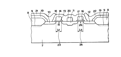
corresponding items and 26 is the channel portion of the
depletion type MOSFET, which is not doped with impurities
of conductivity type opposite to the conductivity type
of the substrate. The fundamental structure thereof is
as follows.
An integrated circuit including the inverter of
E/D structure indicated in Figure 4 comprises a p or n
conductivity type semiconductor substrate 7; a source
region 10 of an enhancement type MOSFET and a drain
region 12 of a depletion type MOSFET formed with a
distance on the principal surface side of the semicon-
ductor substrate; an island-shaped common region 11
acting as a drain region of the enhancement type MOSFET
and a source region of the depletion type MOSFET between
the source region of the enhancement type MOSFET and the
drain region of the depletion type MOSFET; a gate
insulating film 16 for the depletion type MOSFET formed
on the surface portion 15 of the semiconductor substrate
between the drain region of the depletion type MOSFET
and the common region, which portion is not doped with
impurities of conductivity type, which is opposite to
the conductivity type of the semiconductor substrate; a
gate electrode 17 for the depletion type MOSFET formed
on the gate insulated film for the depletion type
P10SFET; an electrode 20 formed on the common region and
connected electrically with the gate electrode for the
depletion type MOSFET; a gate insulating film 13 for the
4
20
enhancement type MOSFET formed on the surface portion 26
of the semiconductor substrate between the source region
of the enhancement type MOSFET and the common region,
which portion is not doped with impurities of conductivity
type, which is opposite to the conductivity type of the
semiconductor substrate; and a gate electrode 14 for the
enhancement type MOSFET formed on the gate insulated
film for the enhancement type MOSFET; wherein at least
- gate electrode for the depletion type MOSFET has a work
function, which is smaller than that of the p conduc-
tivity type semiconductor substrate, in the case where
the semiconductor substrate is of p conductivity type,
and greater than that of the n conductivity type
semiconductor substrate, in the case where the
semiconductor substrate is of n conductivity type.
As the fabrication process of the embodiment
described above, the n MOS process using the well known
LOCOS isolation technique was used. The isolation may
be effected by using any method other than the LOCOS
isolation method. It is required only to be able to
isolate different elements. However, contrarily to the
' well known n P90S process, the part of the p conductivity
type Si 26 just below the gate oxide film l6 in the
depletion type n channel MOSFET is not doped by the ion
implantation, etc. with impurities such as As and P
having the opposite conductivity type. On the other
hand, LaB6 or Mg is used for the gate electrode 17 of
the depletion type n channel MOSFET. The gate made of
LaB6 was formed by using the well known electron beam
evaporation method. That made of Mg was formed by using
zl
the well known electron beam evaporation method or the
sputtering method. The source and the drain region of
the depletion type n channel MOSFET was formed by
implanting ions of P after the formation of the LaB6
gate electrode.
Further, for the gate electrode 14 of the enhance-
ment type MOSFET, the conventional n+ polycrystalline Si
was used.
- Fox example, the LaB6 gate electrode 17 is not
formed by only one layer, as indicated~in Figure 4, but
it may have a two-layered structure consisting of an N+
polycrystalline or silicide layer formed on the LaB6 layer.
In order to control the threshold voltage of the
enhancement type MOSFET, ions of B, which are impurities
of same conductivity type as the p conductivity type Si,
were implanted in the channel portion before the formation
of the gate oxide film 13. The ions of B were implanted
so that the threshold voltage VthE is about 0.7V for an
MOSFET having a channel length of about 0.5um and the
threshold voltage VthE is about +0.3V for an MOSFET
having a channel length of O.lum.
On the other hand, in order to control the
threshold voltage of the depletion type MOSFET, ions~of
B, which are impurities of same conductivity type as the
p conductivity type Si substrate, were implanted in the
channel portion before the formation of the gate oxide
film 2. The ions of B were implanted so that the
threshold voltage VthD is about -2V for an MOSFET having
a channel length of 0.5um and the threshold VthD is
about -1V for an h108FET having a channel length of O.lum.
22
Although in the present embodiment impurities of
same conductivity type as the p conductivity type Si were
implanted for the control of the threshold voltage, the
ion implantation is not necessarily effected, if the
threshold voltages of the enhancement type MOSFET and
the depletion type MOSFET are about 0.2VDD and about
-0.6VDD, respectively, with respect to the source
voltage VDD of the E/D inverter.
If ions of P or As, which are impurities of
conductivity type opposite to the p conductivity type
Si, were implanted in the channel portion at the fabri-
cation of the depletion type MOSFET according to the
prior art technique, although an n type channel is
formed, which performs the depletion type operation at
the room temperature, at the liquid nitrogen temperature
(77K), since P or As impurities implanted as n conduc-
tivity type impurities would be exhausted, no n type
channel layer would be formed and it would not perform
the depletion type operation. However, in the case
where the channel portion is doped with impurities of p
conductivity type with respect to the p conductivity
type Si only for the purpose of varying the concentra-
tion thereof, since they are not frozen out, the freeze
out described previously has influences neither at the
room temperature nor at 77K. Therefore the E/D inverter
according to the present embodiment was able to perform
the normal inverter operation both at the room temperature
and at 77K.
Figures 5B and 6B show in/output characteristics
of the E/D inverters indicated in Figures 5A and 6A
h
23
using P90SFETs having a channel length of about 0.5um and
a~channel length of about O.lum, respectively. The
source voltage VDD is about 3.3V for an inverter having
a channel length of about 0.5um and about 1.5V for an
inverter having a channel length of about O.lum. The in/
output characteristics indicated in Figures 5B and 6B
were obtained both at the room temperature and at 77K.
Contrarily to the fact that the E/D inverter using
conventional depletion type MOSFETs performed no normal
operation at 77K, the E/D inverter according to the
present invention performed the normal operation both at
the room temperature and. at 77K.
A ring oscillator was constructed by connecting
E/D inverters described above in a multi-stage form and
the gate delay time per gate was measured at the room
temperature and at 77K. It was found that it was
shortened about 0.7 to 0.5 time at 77K with respect to
that obtained at the room temperature.
Although in the embodiment described above, p
conductivity type Si was used for the substrate, also in
the case where n conductivity type Si was used for the
substrate, it was possible to construct a depletion type
p channel MOSFET and an inverter of E/D structure without
doping the channel portion of the depletion type MOSFET
with B, which is an impurity of conductivity type opposite
to the n conductivity type Si. For the gate electrode
of the depletion type p channel MOSFET, among materials
having a work function greater than that of the n conduc-
tivity type Si, Se, Ir, Ft, etc. can be used, which are
materials having a work function greater than about
24
5.5ev. However Pt is preferably used, which can be
formed easily by sing the electron beam evaporation
method, etc. and whose melting point is about 1770°C.
By using a gate electrode made of platinum it was possible
to obtain a depletion type MOSFET performing the depletion
operation both at the room temperature and at the low
temperature and to obtain a p channel inverter of E/D
structure.
The depletion type MOSFET according to the
present invention can work both at the room temperature
and at the liquid nitrogen temperature and also the
inverter of E/D structure can work both at the room
temperature and at the liquid nitrogen temperature.
An MOSFET integrated circuit using depletion
type MOSFETs and inverters of E/D structure can provide
a high speed high density integrated circuit provided
both with the high speed of the integrated circuit using
bipolar transistors and with a high degree of integration
of the MOSFET by driving it at the liquid nitrogen
temperature.
Further, contrarily to the inverter of CMOS
structure, the inverter of E/D structure can provide a
high speed high density integrated circuit by using a
simple fabrication process and a small number of MOSFETs.
Furthermore, since the MOSFET integrated circuit
according to the present invention can work both at the
room temperature and at the liquid nitrogen temperature,
at constructing a system it is possible to check the
work thereof at the room temperature to exchange
defective chips and boards, to verify the normal system
h
'~
operation, and thereafter to derive the system with the
highest working performance at the liquid nitrogen
temperature.
P