Note: Descriptions are shown in the official language in which they were submitted.
20t4675
., 1
The present invention relates to a surface
acoustic wave device, and more particularly, it relates to
a surface acoustic wave device which comprises a
piezoelectric substrate and electrodes of aluminum provided
on the piezoelectric substrate.
In recent years, widely employed is a surface
acoustic wave device such as a filter, a resonator or the
like using surface acoustic waves, which may be hereinafter
referred to as SAW.
Such a surface acoustic wave device generally
comprises a piezoelectric substrate, which is provided on
its surface with interdigital transducers and/or grating
reflectors formed by metal strips.
The piezoelectric substrate is prepared from a
single crystal material such as quartz crystal, lithium
tantalate (LiTaO3), lithium niobate (LiNBo3) or lithium
tetraborate (Li2B4O7), or a ZnO/Al2O3) material formed by a
substrate of sapphire (Al2O3) and a film of zinc oxide (ZnO)
provided thereon.
The aforementioned interdigital transducers and
grating reflectors are generally prepared from aluminum,
which is easy to photolithograph and has a small electrode
loading mass effect due to its small specific gravity, and
high conductivity.
However, it has been recognized that, when a
signal of a high voltage level is applied to a surface
acoustic wave device such as a SAW filter or resonator, the
aluminum electrodes are exposed to strong enough stresses
by surface acoustic waves, such as to cause migration.
Such migration caùsed by'stress is called stressmigration,
so as to be distinguished from electromigration. The
resulting stressmigration leads to electrical shorts,
increases in insertion loss, reductions in quality factor
(Q) of the resonator, and the like. Particularly in
surface acoustic wave devices which are used in high
frequency ranges, the stressmiyration more readily occurs
: ' ''
` -
201 4675
as the frequency is increased, and causes significant
problems.
With respect to a resonator, in particular, in
order to cause stable oscillation it is necessary to
increase the gain of an oscillation circuit applying high
voltage level signals. In a resonator having reflectors
which are provided on both sides of one or some
transducers, surface waves are confined between the
reflectors and standing waves are applied to the
transducers and reflectors, to apply strong stress thereto.
Thus, stressmigration is particularly easily caused in the
resonator. To this end, conventional SAW resonators have
been restricted to low voltage levels, in order to keep to
a minimum the stressmigration. Thus, it has been
impossible to increase the C/N ratio (carrier-to-noise
ratio) or to suppress SSB (5ingle-Side-Band) phase noises.
Stressmigration particularly readily occurs in
SAW transmission filters, which receive high voltage signal
levels.
In order to prevent the aforementioned
stressmigration, a small amount of Cu, Ti, Ni, Mg, Pd or
the like is added to the electrode material of aluminum.
However, no satisfactory result has been attained by such
countermeasures.
A substrate of Y-cut (LST-cut) quartz crystal
rotating at an angle of about 105 has been recently
proposed as a substrate for a surface acoustic wave device
having excellent temperature characteristics. The surface
acoustic wave device formed by a substrate of LST-cut
quartz crystal is superior in temperature characterisbics
to that formed by a substrate of ST-cut quartz crystal,
such that leakage surface acoustic waves (LSAW) are
propagated on the surface of the substrate.
However, it is known that, when such an LST-cut
quartz crystal substrate is applied to a resonator, for
example if the thickness of the aluminum electrodes exceeds
1% of the wavelength of the surface acoustic waves, the
~ '~
20 1 4675
operating characteristics deteriorate. No particular
problem is caused when an ST-cut quartz crystal substrate
is employed even if the thickness of aluminum electrodes is
about 2% of the wavelength of the surface acoustic waves.
If the aluminum electrodes provided on the LST-cut crystal
substrate are reduced in thickness in order to avoid
deterioration of the operating characteristics, the
apparent electrical resistivity is increased as the
generally polycrystalline aluminum forming the electrodes
has a large grain size. Thus, insertion loss is increased
and the quality factor is reduced. Such disadvantages are
significant, particularly in the high-frequency range of
short wavelengths.
The inventors have further investigated the cause
for the aforementioned stressmigration. As the result, it
has been recognized that an aluminum film formed through
electron beam deposition, sputtering or the like for
providing electrodes is not crystallographically oriented
in constant directions but is in an amorphous
polycrystalline state. Thus, stressmigration may be caused
by mass transport via grain boundaries in such aluminum
electrodes.
Accordingly, an object of the present invention is
to provide a surface acoustic wave device comprising
aluminum electrodes, which suffer little from the problem
of stressmigration.
The present invention is directed to a surface
acoustic wave device which comprises a piezoelectric
substrate and electrode means provided on the piezoelectric
substrate for forming a transducer, for example, and the
feature of the present invention resides in that the
electrode means includes a film of aluminum which is
crystallographically oriented in constant directions.
It is considered that an aluminum film which is
crystallographically oriented in constant directions
exhibits properties which are similar to those of a single
crystal film. Thus, such an aluminum film buffers very
~ 9 :;:
:
: 20 1 4675
little stressmigration. According to the present
invention, therefore, it is possible to prevent electrical
shorts and the increase in insertion loss caused by
stressmigration. When the present invention is applied to
a resonator, it is possible to prevent reduction of its
quality factor caused by stressmigration.
Thus, the life of the inventive surface acoustic
wave device is prolonged by having suppressed
~stressmigration. In general, significant stressmigration
; 10 occurs with increases in frequency. According to the
present invention, however, such stressmigration can be
suppressed to maintain the surface acoustic wave device in
good characteristics in high-frequency range.
!According to the present invention, further, it is
15 possible to suppress stressmigration even if a high voltage
level signal is applied. Thus, the inventive surface
acoustic wave device can be readily applied to circuits
having high signal levels. When the present invention is
applied to a surface acoustic wave resonator, therefore, it
20 is possible to apply high voltage level signals with no
problem and, accordingly, the C/N ratio can be increased
and SSB phase noises can be reduced. Further, it is
possible to stably oscillate the resonator, which can be
used in an overdriven state with an increased gain. The
25 present invention can also be advantageously applied to
~transmission filters, to which high-voltage signals are
Aapplied.
Preferably the piezoelectric substrate is formed
by a single crystal substrate such as a quartz crystal
30 substrate, a ~iTa~3 substrate, a LiNBo3 substrate or a LilB4O7
`~substrate, or a ZnO/Al2O3 substrate which is prepared by a
ZnO thin film epitaxially grown on a sapphire substrate.
When the piezoelectric substrate is formed by a
quartz crystal substrate, a substrate of rotating Y-cut
35 crystal is preferably employed. When the piezoelectric
substrate is formed of a quartz crystal substrate, an
20 1 ~675
aluminum film is preferably prepared from a (311) oriented
film.
In a preferred embodiment of the present
invention, the angle of rotation of the rotating Y-cut
crystal forming the substrate is selected form within the
range of 25 to 39.
In another preferred embodiment of the present
invention, the angle of rotation of the rotating Y-cut
crystal employed for the substrate is selected from within
the range of 103 to 107. Thus a surface acoustic wave
device is provided that leakage surface acoustic waves are
propagated on its substrate. The aluminum film which is
crystallographically oriented in a constant direction
exhibits properties similar to those of a single crystal
i15 film. Thus, good electrical conduction can be retained
even if the aluminum film is reduced in thickness since it
is not a aggregate of grains. Therefore, it is possible to
effectuate good temperature characteristics originally
provided in the surface acoustic wave device formed by an
LST-cut quartz crystal substrate particularly in a high-
frequency ~omain. Thus, it is possible to implement a
surface acoustic wave device with a substrate of LST-cut
quartz crystal which can be used in a high-frequency
domain.
When the piezoelectric substrate is prepared from
~i2BqO7~ it is preferable to use a substrate of X-cut crystal
rotating at an angle of 45.
A small amount of admixture such as Cu, Ti, Ni, ~ ;
Mg, Pd or the like may be added to the aluminum film, in
order to further effectively~suppress stressmigration. The
content of such an admixture is preferably selected from
within the range of 0.1 to 10 percent by weight. ~;
Embodiments of the invention will now be described
by way of example with reference to the accompanying
35 drawings, in which: ~
.~ ,:
~ :"
20 1 ~67 ~
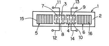
Figure 1 is a plan view showing a surface acoustic
wave device according to an embodiment of the present
invention;
Figure 2 illustrates the transmission response of
, 5 the surface acoustic wave device shown in Figure 1 in 50 n
system;
Figure 3 is a circuit diagram of a system employed
for evaluating power resistance of surface acoustic wave
devices;
10Figure 4 illustrates a curve employed for deciding
the end of life caused by stressmigration;
Figure 5 is an explanatory diagram of a photograph
o~ an aluminum film according ko Example of the pre,sent
invention taken thorough reflection high-energy electron
diffraction (RHEED);
; Figure 6 is an explanatory diagram of a photograph
j of an aluminum film according to reference Example taken
through RHEED;
, Figure 7 is an explanatory diagram of a photograph
1 20 of an aluminum film according to another Example of the
present invention taken through RHEED; and
Figure 8 is a graph showing relation between the
thickness of aluminum electrodes in Example shown in Figure
7 and specific resistance thereof.
25Referring to Figure 1, a surface acoustic wave
device 1 comprises a piezoelectric substrate 2. The
piezoelectric substrate 2 is provided on its surface with,
e.g., two interdigital transducers 3 and 4 and two grating
reflectors 5 and 6 which are positioned to hold the
transducers 3 and ~4. i The interdigital transducer 3
comprises a pair of interdigital electrodes 7 and 8.
Electrode fingers provided in the interdigital electrode 7
are partially opposite to those provided in the
interdigital electrode 8. The interdigital transducer 4 ~ ~;
35 comprises a pair of interdigital electrodes 9 and lO. ~ ~;
Electrode fingers provided in the interdigital electrode 9
are partially opposite to those provided in the
, .~
' :.'
201 ~67')
interdigital electrode 10. Lead terminals 11, 12, 13 and
14 are connected to the interdigital electrodes 7, 8, 9 and
lO respectively.
The reflectors 5 and 6 are formed by grating
electrodes, which are provided with numbers of parallel
metal strips 15 and 16 respectively.
Such a surface acoustic wave device 1 is applicable
to both of a two-port SAW resonator and a two-port SAW
filter. In order to apply the device to a one-port SAW
resonator, one of the transducers 3 and 4 may be omitted.
The reflectors 5 and 6 may be formed by a number of grooves
which are provided on the piezoelectric substrate 2. When
the surface acoustic wave device 1 is applied to a SAW
filter, on the other hand, one of the transducers 3 and 4
;15 serves as an input transducer, and the remaining one serves
as an output transducer. In the case of the filter, the
reflectors 5 and 6 may be omitted. Further, the filter may
be provided with three or more transducers.
~The example of the surface acoustic wave device 1
'l20 shown in Figure 1 is now described in detail along a
sequence of steps of manufacturing the same.
A piezoelectric substrate 2 was formed by a
`lspecularly polished substrate of rotating Y-cut quartz
crystal having an angle of rotation of 33.5. An aluminum
film of about 1000 A in thickness was formed on the surface
of this piezoelectric substrate 2 by means of electron beam
~deposition.
¦In the formation of such aluminum films, the rate
of deposition and the temperature of the substrate 2 have
) 30 generally been selected at 10 A/sec. and +160C~
3 respectively. However, it has been found that the aluminum
film is crystallographically oriented in a constant
direction with an increased rate of deposition and reduced
'~ temperature of the substrate 2. As the result of an
3- 35 experiment made by the inventors, a (311) oriented aluminum
~ film was obtained when the rate of deposition was set at 40
,. ' '~ '.
- 20 ~ 4675
A/sec. and the temperature of the substrate 2 was set at
80OC.
It was confirmed by reflection high energy
eleckron diffraction (RHEED) that the (311) plane of this
aluminum film was epitaxially grown. Figure 5 shows a
drawing of a photograph of the aluminum film take by means
of RHEED.
Referring to Figure 5, numeral 17 denotes a direct
spot of an electron beam, and a reflected pattern is
observed in a region 18. As shown in Figure 5, spots
appear in the reflected pattern due to periodicity of the
crystal structure of the aluminum film. Thus, it can be
confirmed that the aluminum film obtained in the
aforementioned manner was epitaxially grown.
On the other hand, it has also been confirmed that
an aluminum film deposited under the aforementioned
conditions of the rate of deposition of 10 A/sec. and the
substrate temperature of +160C was not epitaxially grown
but was in a random-oriented (amorphous) state. Figure 6
shows an explanatory diagram of a photograph of such
reference example take by means of RHEED.
Referring to Figure 6, numeral 19 denotes a direct
s~ot of an electron beam, and a reflected pattern is
observed in a region 20. No spot appears in the reflected
pattern, which is in the form of a ring or a halo. When
such a ring-shaped or halo-shaped reflected pattern is
obtained, the aluminum film may be evaluated as being
polycrystalline or amorphous.
Both the aforementioned Example of the present
invention and thè reference example were worked in !the
following manner:
An aluminum film was provided by means of
photolithography, to form two interdigital transducers 3
and 4 as well as reflectors 5 and 6 formed by grating
electrodes on the surface of a piezoelectric substrate 2,
as shown in Figure l.
2al 4675
:' g
In a surface acoustic wave device 1 thu~ obtained,
the wavelength of surface acoustic waves was about 4.7 ~m
and the width of each electrode finger was about 1.17 ~m,
while the aperture was about 100 wavelengths. Each of
interdigital electrodes 7, 8, 9 and 10 included in the
` transducers 3 and 4 had 50 electrode fingers, while each of
the refle¢tors 5 and 6 had 300 metal strips.
Figure 2 shows the transmission response of a two-
port SAW resonator in 50 n system according to an Example
obtained in the aforementioned manner. As understood from
Figure 2, the attenuation peak appears at a frequency of
about 674 MHz. Insertion loss at this peak frequency was
about 6 dB. Referring to Figure 2, the left vertical line
represents relative attenuation, with an insertion loss of
0 dB at thP peak frequency. The characteristics of a SAW
resonator prepared according to the reference example were
substantially similar to those shown in Figure 2.
Figure 3 shows a system which was employed ~or
evaluating power resistance, i.e., stressmigration
su~pressibility of both the Example of the present
invention and the reference example. The system shown in
Figure 3 is adapted to power-amplify an output of an
oscillator 21 with a power amplifier 22, whose output is
applied to a SAW resonator 1. An output P(t) of the SAW
resonator l is input to a power meter 23, which measures
the output level thereof. The output of the power meter 23
is fed back to the oscillator 21 through a computer 24,
whereby the frequency of the oscillator 21 is controlled so
that a signal applied to the SAW resonator 1 is regularly
at the peak frequency df transmission response The SAW
, resonator 1 is contained in a thermostatic oven 25, so that
; the SAW resonator l is under a high ambient temperature of
85C, in order to provide a condition for increasing the
I speed for deteriorating the SAW resonator 1.
I 35 The output of the power amplifier 22 was set a 1
` W (50 n system) and an initial output level P0 was measured
to determine that the SAW resonator 1 reached the end of
~
,i. . . : ,: : :
: 201 4675
'. 10
!'~ life td when P(t) < P0 - 1 (dB), where Ptt) represents an
output attained after a lapse of a certain time t. Figure
4 illustrates a yeneral curve of the output P(t). Thus, it
may be proper to estimate that the resonator reaches the
end of life td when the initial output P0 is reduced by 1
dB.
Samples A, B and C were prepared by forming
interdigital transducers 3 and 4 and reflectors 5 and 6
,! with aluminum films made of the following materials:
A: random-oriented pure aluminum
B: random-oriented aluminum containing 1 wt.% of
Cu
C: pure aluminum epitaxially grown.
The samples A and B correspond to the reference
example. The sample B was prepared by adding Cu, which has
; a migration suppressing effect, to aluminum. The sample C
corresponds to the Example of the present invention.
The samples A, B and C were formed of
piezoelectric substrates of quartz crystal having the same
cut angles, and the transducers and reflectors having the
same patterns.
The lifetimes of these samples were evaluated
through the system shown in Figure 3, to attain the
following results:
~¦ 25 A: not more than 5 minutes
B: about 150 minutes
C: at least 900 minutes
~3~ The life of the sample B was longer by about 30
~i times than the sample A due to the effect of the addition
¦ 30 of Cu, while the life of the sample C was increased by ~-
about 6 times over that of the sample B as a result of the
` epitaxial growth of the aluminum film. In other words, the
, life of the sample C, which was prepared from pure
? aluminum, was longer by at least 180 times than that of the
35 sample A, which was also prepared from pure aluminum.
Then Cu, the migration suppressing effect of which
was confirmed by means of sample B, was applied to the
., "
~j :
20 1 ~675
11
sample C. A sample similar to that of sample C was
prepared by forming an aluminum epitaxial film containing
1 percent by weight of Cu. A power application of 1 W
proved to be improper since the life of this sample was too
long. Hence, a power of 2.5 W was applied, in order to
confirm that the sample attained life of at least 8000
minutes. It is generally acknowledged that an acceleration
factor by power is the third or fourth power, and hence the
acceleration factor in relation to power application of 2.5
W is 2.53 or 2.54, i.e., about 15 to about 39 times as
compared to the case of a power application of 1 W. Thus,
a life of at least 8000 minutes attained in the case of the
power application of 2.5 W corresponds to a life of at
least about 120,000 to 312,000 minutes attained in the case
of the application of 1 W of power.
Thus, the life of the aluminum epitaxial film
containing Cu was between 130 and 340 times longer than
that of the pure aluminum epitaxial film. It has been
recognized that Cu may be replaced by Ti, Ni, Mg, Pd or the
like, for achieving a longer life span of the aluminum
film. In general, the content of such an admixture must be
at least 0.1 percent by weight in order to attain a
practical effect, and preferably not more than 10 percent
by weight, so that the resistivity of the aluminum film is
not increased.
I An extremely thin film of Ti, Cr or the like may
be previously formed on the piezoelectric substrate as an
underlayer for the aluminum oriented film in a thickness
I that does not prevent orientation of the aluminum film.
While the aluminum epitaxial film attained (311)
orientation on a substrate of Y-cut quartz crystal rotating
at an angle of 25 to 39, the same may be oriented on a
substrate of crystal rotating at another angle.
In general, the crystal lattices of a substrate
and an aluminum film must substantially conform with each
other in order to attain epitaxial growth of the aluminum
film. Since crystal lattices substantially conform with
201 4675
12
. .
each other between a substrate of Y-cut crystal rotating at
an angle of about 30 and the (311) plane of an aluminum
film, an aluminum film is epitaxially grown on a substrate
of Y-cut quartz crystal rotating at an angle of 25 to 35
in (311) plane orientation. However, the (311) plane of
the aluminum epitaxial film may not necessarily be parallel
to the surface of the crystal substrate. If the cut plane
of the quartz crystal substrate is out of the
aforementioned range of angles, the aluminum epitaxial film
is so oriented that its (311) plane is inclined along the
cut plane of the quartz crystal substrate. Thus, the
aluminum film is oriented in correspondence to the angle of
rotation of the cut crystal forming the substrate, and
hence the material for the crystal substrate is not
particularly restricted to rotating Y-cut quartz crystal.
For example, it is possible to epitaxially grow an aluminum
film on a substrate of doubly rotated cut quartz crystal so
Ithat the (311) plane of the aluminum film substantially
`~satisfies the condition of conformity between the crystal
;~20 lattices.
lIn relation to this, a specularly polished
Isubstrate of Y-cut (LST-cut) crystal rotating at an angle
~of 105 was employed as a piezoelectric substrate, which
`~was treated similarly to the above Example to obtain a
surface acoustic wave device 1 shown in Figure 1. Such a
substrate of Y-cut quartz crystal rotating at 105 has good
temperature characteristics as hereinabove described, while
the quality factor of a resonator is reduced if the
thickness of the aluminum electrodes formed thereon exceeds
1% of the wavelength of the surface acoustic waves.
The aforementioned crystal substrate was applied
to the piezoelectric substrate 2 shown in Figure 1, and an
aluminum film of about 400 A in thickness (about 0.7% of
the wavelength) was formed on the piezoelectric substrate
2 under conditions for electron beam deposition similar to
those in the above Example~ Epitaxial growth of this
aluminum film was confirmed through RHEED. Figure 7 show~
~ .r
201 4675
13
an explanatory diagram of a photograph of the aluminum film
taken through RHEED.
Referring to Figure 7, numeral 26 denotes a direct
spot of an electron beam, and a reflected pattern appears
in a region 27. Spots indicating epitaxial growth of the
aluminum film can be confirmed in this reflected pattern.
The aluminum film was then prepared by means of
photolithography, to prepare a two-port SAW resonator 1
shown in Figure 1. This resonator 1 was similar to that of
the above Example, except that the wavelength of surface
acoustic waves was about 5.9 ~m, the width of each
electrode finger was 1.47 ~m and each of the grating
electrodes forming reflectors 5 and 6 was provided with 500
metal strips.
The SAW resonator 1 exhibited characteristics
which were substantially similar to those shown in Figure
The life of this resonator was evaluated through
the system shown in Figure 3, similar to that of the above
Example.
The life of a sample having transducers 3 and 4
and reflectors 5 and 6 formed from an epitaxial film of
pure aluminum was at least 800 minutes with power
application of 1 W. The life of another sample having
transducers 3 and 4 and reflectors 5 and 6 formed from an
epitaxial aluminum film containing 1 percent by weight of
Cu was too long for a power application of 1 N. This
sample attained life of at least 7000 minutes with power
application of 2.5 W. This life corresponds to that of
between 105,000 and 273,000 minutes attained in the case of
a power application of l W, in accordance with the
aforementioned acceleration factor.
Similarly to the above Example, the amount of Cu
to be added to the aluminum epitaxial film is preferably
between 0.1 and 10 percent by weight. Further, Cu may be
placed by Ti, Ni, Mg, Pd or the like.
.,., : ~.
20 1 4675
An LST-cut crystal substrate of the same type as
above was employed as a piezoelectric substrate, and a
random-oriented aluminum film of 400 A in thickness was
formed on the substrate to similarly prepare a two port SAW
resonator as a reference example. This resonator had large
insertion losses, and exhibited none of the characteristics
which must be provided in a two-port SAW resonator.
Figure 8 shows the relationship between film
thickness and electrical resistivity of both an aluminum
epitaxial film and an aluminum random-oriented film.
Referring to Figure 8, the horizontal line represents the
film thickness (A), and the vertical line represents
specific resistance (n-cm). The solid line shows the
aluminum epitaxial film, and the broken line shows the
~5 aluminum random-oriented film.
As shown in Figure 8, the aluminum epitaxial film
(solid line) retains a low resistivity at a film thickness
of 400 A, while the aluminum random-oriented film (broken
line) exhibits extremely high resistivity at a film
thickness of 400 A. This may be because the aluminum
random-oriented film, which is formed by an aggregate of
,grains, shows an island structure and cannot attain good
electrical conduction when reduced in thickness.
Although the piezoelectric substrate is formed of
`~25 crystal in the above description, the same may
alternatively be prepared from LiNBo3, Li2B4O7, ZnO/Al2O3 or
the like. In the latter case, it is possible to form an
aluminum oriented film by appropriately selecting film
forming conditions and/or a film forming method such as ion
beam sputtering, ion plating or the like. In this case,
the aluminum epitaxial film may not be restricted to a
(311) oriented film, but the crystal orientation of the
aluminum epitaxial film is predetermined so as to satisfy
the required condition as to the conformity of crystal
lattices between the aluminum film and the substrats.
Particularly when the piezoelectric substrate is
prepared from LiTaO3, LiNBo3 or Li2B4O7 having a large
2 0l4 6 75
electromechanical coupling coefficient, it is possible to
implement a S~W filter having a wider band and lower
insertion loss, or a resonator having a small capacitance
ratio as compared with the case of employing a quartz
crystal substrate. A SAW device having a zero temperature
coefficient can be implemented, particularly when a
substrate of X~cut Li2B407 rotating at an angle of 45 is
employed.
Although the present invention has been described
, 10 and illustrated in detail, it is clearly understood that
the same is by way of illustration and example only and is
;not to be taken by way of limitation, the scope of the
present invention being limited only by the terms of the
appended claim~.
t