Note: Descriptions are shown in the official language in which they were submitted.
-
- 1 20 1 4 8 1 ~
This invention relates to an ink jet head which
performs recording by discharging ink responsive to heat
energy generated by an electrothermal transducer, to a
substrate to be used for formation of the head, and to an
ink jet apparatus equipped with the head.
An ink jet system as described in U.S. Patents
4,723,129, 4,740,796, etc. (namely the BUBBLE JET (trade-
mark) system sold by Canon K.K.) can perform recording of
high precision and high quality at high speed and high
density. It is also suitable for recording in color, and
compact implementation, both of which are of increasing
importance in recent years. In a representative example
of a device used in such a system, a direct acting heat
transmitting portion transfers heat to discharge ink
(namely a liquid used for recording) by utilizing heat
energy. By providing a heat-generating resistor having a
direct-acting portion corresponding to an ink pathway,
ink is abruptly heated to form bubbles by utilizing the
heat energy generated from the heat-generating resistor
and ink is discharged through bubble formation.
The direct-acting portion is superficially
similar to the so called thermal head of the prior art
from the standpoint that heat is permitted to act on a
material to be discharged, but the fundamental technique
is greatly different in that the heat-acting portion is
.",~, ~
20 1 48 1 9
-- 2
directly in contact with ink. This means that the
direct-acting portion is exposed to mechanical shock
brought about by cavitation by repeated bubble formation
and bubble extinction in the ink, to other sources of
erosion in some cases.
The direct-acting portion is also exposed to
temperature rises and falls of approximately 1000C
within an extremely short time, of the order of 10~1 to 10
micro-seconds. Therefore, the direct-acting thermal head
technique cannot be applied in BUBBLE JET systems as a
matter of course. Thus, the technology of direct-acting
thermal heads is a category of its own distinct from
basic ink jet techniques.
For forming the heat-generating resistor
constituting the electrothermal transducer of an ink jet
recording head, and because it reaches very high
temperatures, materials are employed which are stable
even at high temperatures and which also have excellent
oxidation resistance, such as nitrides, carbides,
silicides, and borides of high melting point metals or
transition metals.
In recent years, in response to the demands of
high density recording and high speed recording in ink
jet apparatus by use of ink jet recording heads, methods
_- 2014819
-- 3
such as increasing the power applied on heat-generating
resistor or shortening the current pulse width are to be
employed. In such cases, the heat-generating resistor is
heated to even higher temperature, and therefore a heat-
generating resistor having higher heat resistance isdemanded.
When the size of the heat-generating resistor is
made smaller for increasing the recording density, the
area resistance of the heat-generating resistor remains
substantially constant, and therefore only the resistance
value of the electroconductor forming plural heat-
generating resistors as a group is increased, so that the
electric power consumption will be increased in the group
of heat-generating resistors taken as a whole.
Further, power increase requires increased power
capacity of integrated circuits (IC) used to drive the
resistors, which increase of IC capacity in turn
increases the cost of the ink jet head.
Accordingly, in order to meet demands for high
density recording, high speed recording, while reducing
electric power consumption, various methods for enhancing
specific resistance of heat-generating resistor have been
investigated.
'~
20 1 48 1 9
-- 4
For example, as a method for enhancing specific
resistance without changing the shape or the film
thickness of the heat-generating resistor, nitrogen,
oxygen, etc. may be added as a component at a
predetermined ratio in the composition of the heat-
generating resistor in order to obtain a desired specific
resistance.
On the other hand, there is also known a method
of effecting higher resistance by changing the film
thickness of heat-generating resistor without changing
its material.
According to the investigations by the present
inventors of heat-generating resistors made to have
higher resistance by the method of adding nitrogen,
oxygen, etc. as mentioned above, an increase of electric
power consumption accompanied by a great reduction in
resistance value was observed as the driving electric
power was increased. This may be due to the fact that
most of the components added exist dissociated from the
basic heat-generating resistor forming compound.
On the other hand, when specific resistance is
increased by reducing the film thickness of the heat-
generating resistor, and since the film thickness is
required to be closely controlled in this region, a
.~
_ 5 _ 201481'~
problem is involved in maintaining stability of
production. Moreover, the effect of gas and moisture
absorption on the heat-generating resistor surface
appears strongly to worsen the stability of the heat-
generating resistor itself, and therefore the advantageis further reduced as compared with the increase of
resistance of the heat-generating resistor by addition of
nitrogen, oxygen, etc. as described above.
One object of the present invention is to solve
the problems as described above and provide a substrate
for ink jet recording head equipped with an
electrothermal transducer, which can have a high specific
resistance value, produce a stable heat-generating
resistor member with little change in resistance value
accompanied with increase of driving electric power, and
also have excellent durability, an ink jet recording head
comprising the substrate and an ink jet recording
apparatus equipped with the head.
Another object of the present invention is to
provide a substrate for an ink jet recording head
comprising a support and an electrothermal transducer
provided on said support and comprising a heat-generating
resistor member and electrodes electrically connected to
said heat-generating resistor member, wherein said heat-
generating resistor member is comprised of a
- 6 - 20 1 48 1 q
1 complex compound comprising a metal boride, silicon
and nitrogen.
Still another object of the present invention
is to provide an ink jet recording head comprising a
substrate for the ink jet recording head comprising
a support and an electrothermal transducer provided
on said support and comprising a heat-generating
resistor member and electrodes electrically connected
to said heat-generating resistor member, said heat-
generating resistor member being comprised of a complexcompound comprising a metal boride, silicon and nitrogen,
wherein said heat-generating resistor member is used
to generate heat energy to be utilized for discharging
a liquid.
Yet another object of the present invention
is to provide an~in~ jet recording apparatus comprising
an ink jet recording head comprising a substrate for
the ink jet recording head comprising a support and
an electrothermal transducer provided on said support
and comprising a heat-generating resistor member and
electrodes electrically connected to said heat-generating
resistor member, said heat-generating resistor member
being comprised of a complex compound comprising a
metal boride, silicon and nitrogen, and means for carrying
a recording medium, wherein said heat generating resistor
member is used to generate heat energy to
be utilized for discharging a li~uid.
- 7 - 20l 48~
Using the present invention, high quality
recording, high speed recording and low electric power
consumption recording can be realized.
BRIEF DESCRIPTION OF THE DRAWINGS
Fig. 1 is a schematic sectional view showing an
example of the substrate for ink jet head according to
the present invention.
Fig. 2 is a schematic perspective view showing an
example of the principal part of the ink jet head
according to the present invention.
Fig. 3 is a schematic sectional view cut along
the line a-b-c in Fig. 2.
Fig. 4 is a schematic illustration showing the
sputtering apparatus to be used for formation of the
heat-generating resistor layer according to the present
invention .
Fig. 5 is a schematic perspective view showing an
example of the principal part of the ink jet apparatus
equipped with the ink jet head according to the present
invention.
DETATTl~n DESCRIPTION OF THE PREFERRED EMBODIMENTS
The present inventors have studied intensively in
order to address the problems as described above, and
consequently found that the object as mentioned
~- -t ~,
-
2014~9
-- 8
above can be accomplished when the heat-generating
resistor member of ink jet head is constituted of a
complex compound containing 4 elements of a metal
element, boron (B), silicon (Si) and nitrogen (N) at a
specific composition ratio. It has been also found that
the metal element contained in the complex compound
constituting the heat-generating resistor member
according to the present invention should be preferably
at least one element selected from the group consisting
of Ti, V, Cr, Zr, Nb, Mo, Hf, Ta and W, and among them
optimally Hf.
In a complex compound containing the above four
elements in a specific composition ratio, the metal
element is present primarily as a boride, and Si is
present primarily both as a nitride and as native Si
(namely Si-Si bonds are present), as described later; it
may be that these characteristics account for the
extremely good characteristics.
The inventors prepared a number of samples
containing the four elements as described above, in
various composition ratios, by the sputtering method.
Each sample was prepared by means of a sputtering
apparatus as shown in Fig. 4 (sputtering
~,~
201481q
1 Apparatus CFS-8EP, manufactured by Tokuda Seisakusho
Co.) by forming films on a Si single crystal substrate
having a thermally oxidized SiO2 film formed to 5.0 ~m
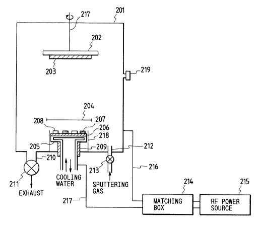
thereon. In Fig. 4, 201 shows a film forming chamber.
202 is a substrate holder for holding the substrate
203 provided within the film forming chamber 201.
The holder 202 has a heater (not shown) for heating
the substrate 203 built therein. The substrate holder
202 is supported by a rotatory shaft 217 extending
from a dirivng motor (not shown) provided outside of
the system, vertically movable and designed so as to
be rotated. At the position opposed to the substrate
203 within the film forming chamber 201 is provided
a target holder 205 for holding a target for film
formation. 206 is a plate metal borlde target of
99.8 wt.% or hig~er purity placed on the surface of
the target holder 205. 207 is a sheet Si target of
99.9 wt.% or higher purity arranged on the metal
boride target. Similarly, 208-lS a sheet Si3N4 target
of 99.9 wt.% or higher purity arranged on the metal
boride target. The Si target 207 and the Si3N4 target
208 are arranged each in a plural number of predeter-
mined area at predetermined intervals on the surface
of the metal boride target 206 as shown in Fig. 4.
Individual areas and arrangements of the Si target
207 and the Si3N4 target 208 are determined on the
basis of a calibration curve, which is prepared by
- 10 201481q
previously defining how the relationship of the area ratio
of the three targets should be made for obtaining a film
containing the four elements at a predetermined composition
ratio.
218 is a protective wall which covers the side faces
of the targets 206, 207 and 208 so that they may not be
sputtered by plasma from their side faces. 204 is a
shutter plate provided so as to be horizontally movable to
shield the space between the substrate 203 and the targets
206, 207 and 208 at the position of the upper part of the
target holder 205. The shutter plate 204 is used as
described below. That is, before initiation of film
formation, it is moved to the upper part of the target
holder 205 holding the targets 206, 207 and 208, an inert
gas such as argon (Ar) gas, etc. is introduced into the
film forming chamber 201 through a gas feeding pipe 212,
the gas is formed into plasma by application of RF power
from a RF power source 215, and the targets 206, 207 and
208 are sputtered with the plasma formed to remove the
impurities on the respective surfaces of the targets.
Then, the shutter plate 204 is moved to the position (not
shown) which does not interfere with film formation.
The RF power source 215 is connected electrically to
the surrounding wall of the film chamber 201 through an
electroconductive wire 216, and also connected electrically
to the target holder 205 through an electroconductive wire
X
11 201 481 9
217. 214 is a matching box.
The target holder 205 is provided with a mechanism
(not shown) which circulates cooling water internally
thereof so that the targets 206, 207 and 208 may be
maintained at desired temperatures during film formation.
In the film forming chamber 201 is provided a discharge
pipe 210 for discharging internally of the film forming
chamber, and the discharge pipe is communicated to a vacuum
pump (not shown) through a discharge valve 211. 202 is a
gas feeding pipe for introducing a gas for sputtering such
as argon gas (Ar gas), helium gas (He gas) into the film
forming chamber 201. 213 is a flow rate controlling valve
for the gas for sputtering provided at the gas feeding
pipe. 209 is an insulator provided between the target
holder 205 and the bottom wall of the film forming chamber
201 for insulating electrically the target holder 205 from
the film forming chamber 201. 219 is a vacuum gauge
provided on the film forming chamber 201. By said vacuum
gauge, the internal pressure in the film forming chamber
201 is automatically detected.
In the device shown in Fig. 4, only one target holder
is provided as described above, but a plurality of target
holders can be also provided. In that case, those target
holders are arranged at equal intervals on concentric
circles at the position opposed to the substrate 203 within
the film forming chamber 201. To the respective target
201 48 1 9
12
holders are connected electrically individually independent
RF power sources through the matching box. In the case as
described above, since three kinds of targets, namely metal
boride target, Si target and Si3N4 target are used, three
target holders are arranged in the film forming chamber 201
as described above, and the respective targets are
individually provided on the respective target holders. In
this case, since predetermined RF powers can be applied
independently on the individual targets, a film in which
one or more of the elements of metal, boron, Si and N is
varied in the film thickness direction can be formed by
varying the composition ratio of the film constituting
elements to be formed into a film.
Each sample formed by use of the device shown in Fig.
4 as described above was prepared according to the film
forming conditions shown below except that the Si target
207 and the Si3N4 target 208 were arranged on the metal
boride target 206 on the basis of the calibration curve
prepared previously about non-single crystalline substance
(film) of the four elements to be obtained.
Substrate arranged on the substrate holder 202:
Si single crystal substrate of 4 inch ~
size having 5.0 ~m thick SiO2 film formed
on the surface (mfd. by Wacker Corp.)
- 13 - 201481~
(3 sheets)
Substrate setting temperature: 50C
Base pressure: 2.6 x 10⁻⁴ Pa or lower
High frequency (RF) power: 500 W
Gas for sputtering and gas pressure:
argon gas, 4 x 10⁻³ Torr
Film forming time: 30 minutes
Of the respective samples obtained as described
above, a partial specimen of the samples were subjected
to compositional analysis by performing X-ray
photoelectric spectroscopic analysis by means of ESCA-750
manufactured by Shimadzu Corp.
Next, for each sample, by use of another
specimen, film thickness and specific resistance were
measured, and further by use of still another specimen, a
step stress test (SST) for observation of heat resistance
and impact resistance, etc. was conducted. SST was
conducted according to the same manner as the step stress
test as described later. As the result of overall
investigation of these results, the following conclusions
were obtained.
The above-mentioned problems can be alleviated
dramatically to give a heat-generating resistor member
particularly excellent in high temperature stability with
high resistance, and which is also equal to or better
than the prior art in durability when the complex
compound constituting the heat-generating
., .
- 14 - ~ 2 Ol 4~l q
1 resistor member of an ink jet head contains the following
four elements at a specific composition shown below.
8 atomic % < metal element < 31 atomic %
7 atomic % < B < 58 atomic %
5 atomic % < Si< 53 atomic %
6 atomic % ~ N < 45 atomic %.
As the specific composition ratios of the four
elements, the following ranges are preferred:
15 atomic % ~ metal atom ~ 24 atomic %
18 atomic % ~ B ~ 38 atomic %
19 atomic % < Si < 35 atomic %
18 atomic % < N ~ 38 atomic %.
Further, it is preferable for obtaining a heat-
generating resistor member of high resistance and excellent
high temperature stability that the ratio of numbers
of atoms of Si tq N-contained in the complex compound
constituting the heat-generating resistor member be
within the following range:
0.6 ~ Si/N ~ 2.5
In addition, the ratio of numbers of atoms of
Si to N is further preferably as follows:
0.7 ~ Si/N ~ 1.3.
The heat-generating resistor member according
to the present invention can be formed with a desired
thickness on a support according to various thin film
forming techniques such as the vapor deposition method,
the sputtering method, the CVD method, etc. by use of
2014819
1 starting materials capable of supplying the respective
constituents of the complex compound as described above.
Referring now to the drawings, the present
invention is described in detail.
Fig. 1 is a partial sectional view showing the
structure of an example of the substrate for an ink
jet recording head of the present invention.
The substrate has a structure, comprising an
electrothermal transducer having a heat-generating
resistor member 2 and a pair of opposed electrodes 3,
4 and a protective layer 5 provided on a support 1
formed by use of an insulating material such as
silicon oxide, glass or ceramics, or a silicon single
crystal member having a SiO2 layer formed by thermal
oxidation on the surface, etc.
The heat.generating resistor member 2 is formed
of a thin film of the complex compound as described
above. The portion of the heat-generating resistor
member 2 between the electrodes 3, 4 forms a heat-
generating portion 2a which genera~es heat by currentpassage between the electrodes 3, 4. The electrodes
3, 4 are formed of good conductor as represented by
metals such as Al, Au and Cu.
The protective film 5 has the function of
protecting the portion positioned immediately below
the liquid pathway of the electrothermal transducer
possessed by the ink jet recording head prepared by
- 16 201 481~
use of the substrate against contact with ink, and can be
formed of an insulating material such as SiO2, SiC or SiN,
etc.
The protective film 5 is not necessarily required to
be formed of a single material, but may be also one having
the multi-layer film constitution of the above-mentioned
materials, or a structure provided with a metal thin film
layer for cavitation resistance such as Ta on the outermost
surface in contact with a liquid (ink, etc.).
The heat-generating resistor member 2 can be formed by
subjecting a thin film comprising the above-described
complex compound to patterning according to an appropriate
patterning method such as photolithographic steps, etc.
Its film thickness and width, the interval of the
electrodes 3, 4, etc. may be chosen selectively so that
necessary characteristics can be obtained at the heat-
generating portion of the thin film heat-generating
resistor member corresponding to the design of the required
ink jet recording head.
The thin film comprising the complex compound has the
advantage that the desired high specific resistance value
can be obtained under high driving power even when it is
made a film having a thickness relatively easier in film
thickness control (e.g. 500 A - 5 ~m). The thickness of
the layer of the
` - -
- 17 - 201481~
heat-generating resistor member according to the present
invention may be preferably 300 A to 2 ~m, more
preferably 700 A to 1 ~m, optimally 1000 A to 5000 A.
On the substrate with the constitution shown in
Fig. 1 can be formed at least a liquid pathway
communicated to a discharge opening to give the ink jet
recording head of the present invention.
Fig. 2 and Fig. 3 show the basic structures of
the pertinent portion of an example of the ink jet
recording head according to the present invention
respectively as a schematic perspective view and a
schematic sectional view.
In this example, on the substrate for ink jet
with the above-described constitution are provided a
partition wall 6 for providing the liquid pathway 9
communicated to the discharge opening 8 corresponding to
the heat-generating portion 2a of the electrothermal
transducer and a ceiling plate 7 for covering over the
partitioning wall.
The partition wall 6 can be formed by use of a
material with excellent liquid penetration and liquid
resistance characteristics selected from organic
insulating materials, having, for example, photo-
sensitivity such as epoxy resin, polyimide resin, phenol
resin, etc., according to the known methods such as a
method including photolithographic steps.
In Fig. 2, the discharge units for ink discharge
'1 ~' 7
~ A~
. . . ~
- 18 - 2 0 1 4 8 1 q
including discharge opening, liquid pathway, heat-
generating portion 2a of electrothermal transducer are
sectionalized by the partition walls 6 to form the
multiple discharge units.
The ceiling plate 7 is the portion corresponding
to the ceiling of the liquid pathway in each discharge
unit, and can be formed of a material selected from
glass, metal, ceramic, plastic, etc.
For bonding between the partition wall 6 and the
ceiling plate 7, bonding by use of an adhesive such as
epoxy resin or cyanoacrylate resin, etc. can be utilized.
In this ink jet recording head, since the above-
described complex compound with excellent high
temperature stability and high resistance is used as the
material for the heat-generating resistor member, the
recording head has a constitution which can sufficiently
correspond to the demands of high density recording and
high speed recording.
The configuration of the heat-generating resistor
member of the present invention are not limited to the
example as described above, but can take various
configurations.
For example, the recording head shown in the
drawings has a construction in which the direction in
which the liquid is fed to the heat-generating portion
and the direction in which the liquid is discharged
-19- 2014819
1 from the discharge opening are substantially the same,
but it may also have a constitution in which these
directions are different from each other, for example,
forming substantially right angle therebetween.
Example 1
A support provided with a SiO2 layer of 5.0 ~m
film thickness by thermal oxidation treatment of the
surface of a Si single crystal substrate was placed
at a predetermined position within the RF sputtering
apparatus as described above shown in Fig. 4, and
further a Si3N4 chip (purity: 99.9 wt.% or higher)
and a Si chip (purity: 99.9 wt.% or higher) were
placed on a HfB2 target of 5 inch in diameter
(purity: 99.8 wt.% or higher) respectively at area
ratios of 25 % and 10 % to the target, and film
formation was effected on the SiO2 layer of the
support by sputtering under the conditions of a
power during discharging of 0.5 kW, an Ar pressure
during discharge of 4 x 10 3 torr for 30 minutes.
The composition of the hea~-generating resistor
thin film obtained was analyzed by XPS (X-ray photo-
electric spectrophotometry) under the state after the
surface contaminated layer was removed by Ar ion
sputtering. The quantitative analytical values are
shown in Table 1. Also, the film composition expressed
in atomic % (rounded to the nearest whole number) is
shown in Table 2.
-
- 20 - 2014819
1 Table 1
Hf B Si N
Atomic ratio 1.00 1.80 1.04 0.92
Further, by the same analytical apparatus the
bonding states of the principal elements were judged.
As the result, it may be considered that, since
the 4f orbital electron peak bonding energy of Hf is
found at 15.9 eV, Hf has formed primarily a boride,
while since the 2p orbital electron peak energy of
Si is found at 99.0 eV, Si contains primarily the
state of nitride and the same state as Si single
substance (namely the state of Si - Si bond). B
and N may be considered to have each formed boride
and nitride (namely compounds), since the ls orbital
bonding energies are found at 187.0 eV and 397.0 eV.
When the film thickness and the specific
resistance of the heat-generatlng resistor thin film
obtained were measured in conventi~nal manner, they
were found to be 1420 A and 1150 Q-cm, respectively.
Next, on the heat-generating resistor thin
film on the support, further was laminated an Al
layer of 5000 A by electron beam vapor deposition,
and these were subjected to patterning to a wiring
width of 30 ~m according to the photolithographic
steps, followed further by removal of the portion
-
- 21 - 201 481 ~
1 corresponding to the heat-generating portion 2a of the
electrode layer (30 ~m x 150 ~m) to form an electro-
thermal transducer.
Further, a SiO2 layer (layer thickness 2.0 ~m)
covering over the electrothermal transducer was formed
as the protective layer 5 by RF sputtering to obtain
a substrate for ink jet head having the constitution
shown in Fig. 1. The respective electrodes 3, 4 were
provided with terminals (not shown) for receiving the
signals from the outside connected thereto.
Next, partition walls 6 (height 50~m) comprising
a photosensitive polyimide resin in conventional manner
including photolithographic steps so that the liquid
pathways communicated to the discharge openings 8 may
lS be positioned at the positions corresponding to the
respective heat-generating portions, and further the
glass plates 7 with a thickness of 1 mm covering over
the partition walls were bonded by use of an epoxy
resin to give an ink jet recordlng head with the
constitution shown in Fig. 2 and Fi~. 3.
On the heat-generating portion 2a of the ink
jet recording head obtained, a rectangular pulse wave
of 7 ~s was applied at 3 kHz, and the application
voltage was gradually raised by use of pure water as
the recording liquid to determine the voltage at
which bubble formation is initiated.
Next, a rectangular pulse wave of 3 kHz was
2014819
~ 22
applied so that the pulse voltage value became greater by
1.0 V in every 2 minutes, and the change in the heat-
generating resistor value (aR) was measured until the heat-
generating resistor was broken. This test method is called
~ 5 step stress test (SST), and according to this test, the
life including heat resistance, impact resistance under
real driving state of an ink jet recording head can be
evaluated.
10From the results obtained and the resistance value Ro
before practice of the test, resistance change rate (aR/Ro)
were calculated. As the result, the heat-generating
- resistor member according to this Example exhibited
excellent characteristics with the resistance value change
immediately before breaking being small as + 5.0 ~.
Besides, in the heat-generating resistor member according
to this Example, the consumption current was sufficiently
small at 136 mA. Hence, it has been found that the
consumption power can be small and therefore an IC for
driving with small capacity can be sufficiently effective.
Also, the margin M (application voltage immediately
before breaking/application voltage at initiation of bubble
formation) in the ink jet head of this Example was found to
be 1.58, thus exhibiting sufficient heat resistance and
impact resistance.
Further, when printing was practiced by use of the ink
X
~ 23 201 48l9
jet head according to this Example, good printing quality
could be obtained.
The evaluation results of Example 1 as described are
summarized in Table 2.
Examples 2 - 12
According to the same procedure as in Example 1 except
for varying variously the area ratios of the targets, heat-
generating resistor thin films with various compositions
were formed on supports, and then the ink jet heads shown
in Fig. 2 and Fig. 3 were prepared in the same manner as
described in Example 1.
For the respective Examples, various data were
determined in the same manner as in Example 1, and the
results are shown in Table 2. As can be seen from Table 2,
all ink jet heads according to these Examples exhibited
sufficiently great specific resistance values and
sufficiently small resistance change rates, sufficiently
small consumption currents, and further sufficient heat
resistance and impact resistance.
Also, when printing was practiced by use of the ink
jet recording heads according to the respective Examples,
good printing quality could be obtained in all of the
Examples.
Comparative Examples 1 - 7
According to the same procedure as in Example 1 except
for varying the area ratios of the targets, heat-generating
resistor thin films having
X
__
- 24 - 2 0 1 4 8 1 ~
1 various compositions were formed on supports. Then,
the ink jet recording head shown in Fig. 2 and Fig.
3 were prepared in the same manner as in Example 1.
For respective Comparative Examples, various
date were determined in the same manner as in Example
1, and the results are shown in Table 2. As can be
seen from Table 2, the ink jet heads according to
these Comparative Examples exhibited the results
which could not be said to be necessarily satisfactory
in either of evaluations of specific resistance value,
resistance change rate, consumption current, heat
resistance and impact resistance.
Example 13
Formation of a heat-generating resistor thin
film onto a support was performed by the RF magnetron
simultaneous sputtering under the same conditions as
in Example 1 except for using HfB2 and Si (area ratio
relative to HfB2 target of 25 %), and flowing N2 gas
at 0.5 SCCM into the Ar gas for sputter (gas pressure
4 x 10 3 Torr) while mixing therewifth.
The heat-generating resistor thin film had a
film thickness of 1995 A and a specific resistance
value of 968 ~ cm.
By use of the heat-generating resistor thin
film obtained, an ink jet recording head was prepared
in the same manner as described in Example 1.
For this Example, various data were determined
20 1 48 1 ~
_ 25
in the same manner as in Example 1, and the results are
shown in Table 3. As can be seen from Table 3, also the
ink jet head according to this Example exhibited
sufficiently great specific resistance value and
sufficiently small resistance change rate, sufficiently
small consumption current, and further, sufficient heat
resistance and impact resistance.
Also, when printing was practiced by use of the ink
jet head according to this Example, good printing quality
could be obtained.
Examples 14 - 16
According to the same procedure as in Example 13
except for varying the area ratios of the targets and the
flow rate of N2, heat-generating resistor thin films having
various compositions were formed on supports. Then, the
ink jet heads shown in Fig. 2 and Fig. 3 were prepared in
the same manner as in Example 13.
For the respective Examples, various data were
determined in the same manner as in Example 13, and the
results are shown in Table 3. As can be seen from Table 3,
all the ink jet heads according to the Examples exhibited
sufficiently great specific resistance values and
sufficiently small resistance change rates, sufficiently
small consumption currents and further, sufficient heat
resistance and impact resistance.
Also, when printing was practiced
O;~ ~
.
,~
- 26 - ' 2014819
1 by use of the ink jet heads according to the respective
examples, good printing quality could be obtained in
all the Examples.
Comparative Examples 8, 9
According to the same procedure as in Example
13 except for varying variously the area ratios of the
targets and the flow rate of N2, heat-generating resistor
thin films having various compositions were formed on
supports. Then, the ink jet heads shown in Fig. 2 and
Fig. 3 were prepared in the same manner as in Example
13.
For the respective Comparative Examples,
various data were determined in the same manner as in
Example 1, and the results are shown in Table 3. As
can be seen from Table 3, the ink jet heads according
to these Comparative Examples exhibited the results
which could not be said to be necessarily satisfactory
in evaluation of either of specific resistance value,
resistance change rate, consumptlon current, heat
20 resistance and impact resistance.
Other Examples and Comparative Examples (Part 1)
According to the same procedure as described
in Examples 1 to 16 and Comparative Examples 1 to 9
except for using TiB2 in place of HfB2 as metal boride,
25 the ink jet heads shown in Fig. 2 and Fig. 3 having
the heat-generating resistor member of the present
invention were prepared.
27 20l 48lq
All of the ink jet heads according to the Examples
exhibited sufficiently great specific resistance values and
sufficiently small resistance change rates, sufficiently
small consumption current, and further, sufficient head
resistance and impact resistance.
Also, when printing was carried out by use of the ink
jet heads according to the respective Examples, good
printing quality could be obtained in all of the Examples.
On the other hand, the ink jet heads according to
Comparative Examples exhibited the results which could not
be said to be necessarily satisfactory in either of the
evaluations of specific resistance value, resistance change
rate, consumption current, heat resistance and impact
resistance.
Other Examples and Comparative Examples (Part 2)
According to the same procedure as described in
Examples 1 to 16 and Comparative Examples 1 to 9 except for
using VB2 in place of HfB2 as metal boride, the ink jet
heads shown in Fig. 2 and Fig. 3 having the heat-generating
resistor member of the present invention were prepared.
All of the ink jet heads according to the Examples
exhibited sufficiently great specific resistance values and
sufficiently small resistance change rates, sufficiently
small consumption current, and further, sufficient heat
resistance and impact resistance.
X
~ 201 481q
28
Also, when printing was carried out by use of the ink
jet heads according to the respective Examples, good
printing quality could be obtained in all of the Examples.
On the other hand, the ink jet heads according to
Comparative Examples exhibited the results which could not
be said to be necessarily satisfactory in either of the
evaluations of specific resistance value, resistance change
rate, consumption current, heat resistance and impact
resistance.
Other Examples and Comparative Examples (Part 3)
According to the same procedure as described in
Examples 1 to 16 and Comparative Examples 1 to 9 except for
using CrB2 in place of HfB2 as metal boride, the ink jet
heads shown in Fig. 2 and Fig. 3 having the heat-generating
resistor member of the present invention were prepared.
All of the ink jet heads according to the Examples
exhibited sufficiently great specific resistance values and
sufficiently small resistance change rates, sufficiently
small consumption current, and further, sufficient heat
resistance and impact resistance.
Also, when printing was practically carried out by use
of the ink jet heads according to the respective Examples,
good printing quality could be obtained in all of the
Examples.
2014819
_. 29
On the other hand, the ink jet heads according to
Comparative Examples exhibited the results which could not
be said to be necessarily satisfactory in either of the
evaluations of specific resistance value, resistance change
rate, consumption current, heat resistance and impact
resistance.
Other Examples and Comparative Examples (Part 4)
According to the same procedure as described in
Examples 1 to 16 and Comparative Examples 1 to 9 except for
using ZrB2 in place of HfB2 as metal boride, the ink jet
heads shown in Fig. 2 and Fig. 3 having the heat-generating
resistor member of the present invention were prepared.
All of the ink jet heads according to the Examples
exhibited sufficiently great specific resistance values and
sufficiently small resistance change rates, sufficiently
small consumption current, and further, sufficient heat
resistance and impact resistance.
Also, when printing was carried out by use of the ink
jet heads according to the respective Examples, good
printing quality could be obtained in all of the Examples.
On the other hand, the ink jet heads according to
Comparative Examples exhibited the results which could not
be said to be necessarily satisfactory in either of the
evaluations of specific resistance value, resistance change
rate, consumption current, heat resistance and impact
resistance.
;, ~,
2014819
_ 30
Other Examples and Comparative Examples (Part 5)
According to the same procedure as described in
Examples 1 to 16 and Comparative Examples 1 to 9 except for
using NbB2 in place of HfB2 as metal boride, the ink jet
heads shown in Fig. 2 and Fig. 3 having the heat-generating
resistor member of the present invention were prepared.
All of the ink jet heads according to the Examples
exhibited sufficiently great specific resistance values and
sufficiently small resistance change rates, sufficiently
small consumption current, and further, sufficient heat
resistance and impact resistance.
Also, when printing was practiced by use of the ink
jet heads according to the respective Examples, good
printing quality could be obtained in all of the Examples.
On the other hand, the ink jet heads according to
Comparative Examples exhibited the results which could not
be said to be necessarily satisfactory in either of the
evaluations of specific resistance value, resistance change
rate, consumption current, heat resistance and impact
resistance.
Other Examples and Comparative Examples (Part 6)
According to the same procedure as described in
Examples 1 to 16 and Comparative Examples 1 to 9 except for
using Mo2B5 in place of HfB2 as metal boride, the ink jet
heads shown in Fig. 2 and Fig. 3 having the heat-generating
resistor members of the present invention were prepared.
_ 31 20 1 48 1 9
All of the ink jet heads according to the Examples
exhibited sufficiently great specific resistance values and
sufficiently small resistance change rates, sufficiently
small consumption current, and further, sufficient heat
resistance and impact resistance.
Also, when printing was carried out by use of the ink
jet heads according to the respective Examples, good
printing quality could be obtained in all of the Examples.
On the other hand, the ink jet heads according to
Comparative Examples exhibited the results which could not
be said to be necessarily satisfactory in either of the
evaluations of specific resistance value, resistance change
rate, consumption current, heat resistance and impact
resistance.
Other Examples and Comparative Examples (Part 7)
According to the same procedure as described in
Examples 1 to 16 and Comparative Examples 1 to 9 except for
using TaB2 in place of HfB2 as metal boride, the ink jet
heads shown in Fig. 2 and Fig. 3 having the heat-generating
resistor member of the present invention were prepared.
All of the ink jet heads according to the Examples
exhibited sufficiently great specific resistance values and
sufficiently small resistance change rates, sufficiently
small consumption current, and further, sufficient heat
resistance and impact resistance.
201 48 1 9
_ 32
Also, when printing was carried out by use of the ink
jet heads according to the respective Examples, good
printing quality could be obtained in all of the Examples.
On the other hand, the ink jet heads according to
Comparative Examples exhibited the results which could not
be said to be necessarily satisfactory in either of the
evaluations of specific resistance value, resistance change
rate, consumption current, heat resistance and impact
resistance.
Other Examples and Comparative Examples (Part 8)
According to the same procedures as described in
Examples 1 to 16 and Comparative Examples 1 to 9 except for
using W2Bs in place of HfB2 as metal boride, the ink jet
heads shown in Fig. 2 and Fig. 3 having the heat-generating
resistor members of the present invention were prepared.
All of the ink jet heads according to the Examples
exhibited sufficiently great specific resistance values and
sufficiently small resistance change rates, sufficiently
small consumption current, and further, sufficient heat
resistance and impact resistance.
Also, when printing was carried out by use of the ink
jet heads according to the respective Examples, good
printing quality could be obtained in all of the Examples.
On the other hand, the ink jet heads according to
Comparative Examples exhibited the results which could not
be said to be necessarily satisfactory in either of the
evaluations of specific resistancé value, resistance change
~,
~ 33 2014819
rate, consumption current, heat resistance and impact
resistance.
The standards for the overall evaluation shown in Fig.
2 and Fig. 3 are shown in Table 4.
The heat-generating resistor member according to the
present invention has high resistance value and small
consumption power as described above, and therefore is
particularly effective when used for an ink jet head of the
form having functional elements provided structurally
internally of the head substrate as disclosed in U.S.
Patent 4,429,321.
By mounting the ink jet head according to the present
invention having the constitution as described above on a
main apparatus and imparting signals to the head from the
main apparatus an ink jet recording apparatus capable of
performing high speed recording and high image quality
recording can be obtained.
Fig. 5 is a schematic perspective view showing an
example of a jet recording apparatus IJRA to which
'~ I'
~ 34 ~ 2014819
1 the present invention is applied, and the carriage HC
engaged with the spiral groove 5004 of a lead screw
5005 which rotates through driving force transmitting
gears 5011, 5009 in associated movement with normal
and reverse rotations of a driving motor 5013 has a
pin (not shown) and is moved reciprocally in the
directions of the arrows a, b. 5002 is a paper
pressing plate, which presses paper over the carriage
movement direction against a platen 5000. 5007, 5008
are photocouplers, which are home position detecting
means for effecting rotation direction change-over of
the motor 5013 by confirming the presence of a lever
5006 of the carriage in this region. 5016 is a member
for supporting a cap member 5022 which caps the front
face of a recording head IJC of the cartridge type with
an ink tank provided integrally, and 5015 is an aspira-
tion means which aspirates internally of the cap which
performs aspiration restoration of the recording head
through an opening 5023 within^the cap. 5017 is a
cleaning blade, 5019 is a member wh~ch enables movement
of the blade in the direction of back and forth, and
these are supported on a main body supporting plate
5018. The blade is not required to be in this form,
but any cleaning blade well known in the art is
applicable to this example, as a matter of course.
5012 is a lever for initiating aspiration of the
aspiration restoration, which moves as accompanied
- 35 ~ 20 1 48 1 9
with the movement with a cam 5020 engaged with the
carriage, with the driving force from the driving
motor being controlled by known transmission means
such as clutch change-over, etc. A CPU which
imparts signals to the electrothermal transducer
provided at the ink jet head IJC, and controls
driving of the respective mechanisms as described
above is provided on the main body side (not shown).
In the examples of the present invention as
described above, description is made by use of a
liquid ink, but in the present invention, even an
ink which is solid at room temperature can be used,
provided it is softened at room temperature. In the
ink jet apparatus as described above, temperature
control is generally practised so that ink viscosity
is within stable discharge range by controlling the
temperature within the range of 30C to 70C, and
therefore any ink may be used which becomes liquid
when the apparatus is subjected to working
conditions. Arrangements may be used in which
temperature elevation by the application of thermal
energy is prevented by permitting it to be used as
the energy for a phase change from the solid state
to the liquid state, or in which an ink is used
' `....1 .
.., ... , . .
2014819
- 36 -
which is solidified in the rest state of the
apparatus for the purpose of preventing evaporation
of ink, or in which an ink is used having the
property that it is liquefied for the first time by
thermal energy, such as one which is liquefied by
imparting thermal energy corresponding to the
recording signals but has already commenced to
solidify when it reaches the recording medium. In
such a case, the ink may be located adjacent the
electrothermal transducer in liquid or solid state
at a porous sheet concavity or thru-hole as shown in
Japanese Laid-Open Patent Applications Nos. 54-56847
and 60-71260. In the present invention, the
arrangement which is the most effective for the
respective inks mentioned above is that which
practices the film boiling system as described
above.
The construction and operation of the
recording head, and the recording apparatus of an
ink jet system according to the present invention
may be, by way of preferred example, basically in
accordance with the disclosures of U.S. Patents
4,723,129 and 4,740,796. This system is applicable
to operation either of the so called on-demand type
and the continuous type. The on-demand type is
particularly effective because, by applying at least
_ 37 _ 2 0 1 4 8 1 9
one driving signal which gives rapid temperature
elevation exceeding nucleus boiling point,
corresponding to the recording information, to
electricity-heat convertors arranged corresponding
to the sheets or liquid channels holding liquid ink,
heat energy is generated at the electricity-heat
convertors to effect film boiling at the direct-
acting surface of the recording head, and
consequently the bubbles within the liquid ink can
be formed in one-to-one correspondence to the
driving signals. By discharging the liquid ink
through a discharge opening by growth and shrinkage
of the bubble, at least one droplet is formed. By
forming the driving signals into pulses, growth and
shrinkage of the bubble can be effected almost
instantaneously and adequately to accomplish
discharge of the liquid ink with a particularly
excellent response characteristic. As the driving
signals of such pulse shapes as those disclosed in
U.S. Patents 4,463,359 and 4,345,262 are suitable.
Excellent recording can be performed by employment
of the conditions described in U.S. Patent 4,313,124
in respect of the temperature elevation rate of the
above-mentioned direct-acting surface.
The construction of the recording head, in
addition to the combined features of discharging
~,,~,. ..
....
2014819
- 38 -
orifice, liquid channel, electricity-heat converter
(linear liquid channel or right angle liquid
channel) as disclosed in the above-mentioned
respective specifications, may incorporate the
features of U.S. Patents 4,558,333, 4,459,600 which
disclose having the heat transfer portion arranged
in a bent portion of the channel. In addition, the
present invention can also effectively employ the
structure disclosed in Japanese Patent Laid-Open
Application No. 59-123670, which discloses using a
slit common to a plurality of electricity-heat
convertors as the discharging portion of the
electricity-heat converter, or Japanese Patent Laid-
Open Application No. 59-138461 which discloses
having an opening for absorbing pressure waves
generated by heat energy, associated with the
discharging portion.
Further, in a recording head of the full
line type having a length corresponding to the
maximum width of recording medium which can be
recorded by the recording device, either a
construction which provides its length by
combination of a plurality of recording heads as
disclosed in the above-mentioned specifications or a
construction as one recording head, integrally
formed, may be effectively used in the present
,
,
," ~
- 39 -
invention. 2 0 1 4 8 1 9
In addition, the present invention is
effective in a recording head of the freely
exchangeable chip type which enables electrical
connection to the main device or supply of ink from
the main device by being mounted on the main device,
or in a recording head of the cartridge type where
it is provided integrally on the recording head
itself.
The addition of auxiliary components to the
recording head is usually preferred so that the
effect of the present invention can be further
stabilized. Specific examples may include, for the
recording head, capping means, cleaning means,
pressurization or aspiration means, electricity-heat
convertors or other heating elements, pre-heating
means, or any combination of these. The invention
is also effective for performing stable recording in
a preliminary mode in which discharging is performed
separate from recording.
Further, according to the recording mode of
the recording device, the present invention is
extremely effective not only for recording in a
primary single color such as black, but also in a
: . ;; ,.
201 4819
- 40 -
device equipped with selectable plural different
colors or full color by color mixing, whether the
recording head is integrally constituted or several
heads are combined.
_ 41 - 201 481 9
~ _ I o a~ ~ ~ ~ ~ ~ u~ ~ In ~ ~ ao o ~ o o o In
n ............ .......
0 C ~ ~ ~ ~ d' d' a~ t--~ ~r o c~ 1 0 ~
-
~1 C,)
~ I O O 1--Lfl ~ ~ d' t--~ O ~ 1-- 0 0 ~ O ~ 1-- 0
~ 0 ~a ~ o~ ~ODmO~
~ 0 C
U)~
o o~ ~ ~ In o u~ o ~ o o o ~D 1`
~ ~ 0 d ~ N ~ 10 ~ ~ (~) ~ ~1 0 ~ t~ ~ t~ ~ d'
Z ~ ~ ~ ~ ~ o ~ o t--~ o~ ~ ~ ~ ~ ~ ~n
~ O O ~ ~ ~ O ~ ~ O ~ O O O O ~ O
p
~ u~ -
~ ~ ~~ o In 00 ~n o ~ ~ In r~
20 h a) ~ C~
~ ,n o o o o o o o o o o o .,, o ~ o o ~ o
a
O O ~ ~ ~ ~ m ~ r~ co ~ o ~ ~ ~ ~ ~ ~ ~ ~ ~g ~~
J ~ ~ S2.,
~ _ ~ X
-42- 201481q
,_~ ~
~ ~ 0
~: 0 ~
- 0 ~ 0 ~ ~ 0 0 ~ ~ 0 0 00 ~
-, O
o
~n ~: ............ .......
15 p
E~ ~ ,,
C O -I ~ ~ o ~ 1` ~ ~ ~ co o~
C~ ~ V
x
a~
.
z z ~ ~ ~ ~ x c~ o ~' ~
a) ~ a~ a
E
~ ~ 0
~X r ~1 X X
F~ V ~ V
-
-- 43 --
20 1 48 1 9
U~ ~ o ..~ o o
~ O ~
o ~ ~ ~ ~ ~ _ _
,1 s
E~ .
_ _ _ o
--~
C ~ C~ C~
C~ ~ Z
r~
~~ 3
p~ o C~ , ........ . .
^-- ~0O æ
~ ~~ n o o o o
C ~ ~ ~ ~
4 "~ .
Z ~ .
-
-- 44 --
~01 4319
~ ~ O /(~
o
a ~
o _
O ~ o
n,
~ n ~ o c~~ u~ o o
a) w
Q ~Y cJ v I
rl C~ ~ O ~ :~ O O
,1 n ~- cn ~ o ~ CD ~o
w u~ w ~
~ ~
w ,~ ~ r~l -~
:z j ;
20 1 4~ 1 9
- 45 -
h h
O O C:
Et
U~ ~ h h ~
o 0 0
In ~r 0
0
O 0 0
0 s
h h
~ ~ O h a) O
0 ~ O ~0
O ~ l-- o
CJ ~) ~ o h
O
U 0
o~ a) a.~ ~1 0 4-1
1~ a) JJ ~J O 0 ~' O h
0 tJ7 ~ ) r~l a) ~J
O ~ O ~.~ O
0 ~ o u~ ~ 0 ~ 0 r~
a).~ Q 11~ P
V ~ r~ rS r O
~0
15 ~ C
E~
a
h h
O ~ ' O O ~:
h S
4~ ~ O O
~ ~ ~ o o 0
U~ ~ ~
. . ~
c a~
o ~ U~ ~) ~ C~
O
O
~ s
~ S -~ 4~ ~ S ~ S
3 t~ ~ O u~ 3 ~~
~ O -~1 O a) ~1 0 o ~ h O
~ S ~ '~ C ~ ~
S ~ S ~ O S ~ ~ O
o l~ u~ h ~ ~ ~ ~ O O