Note: Descriptions are shown in the official language in which they were submitted.
201~2
ACKGROUND OF THE INVE~TIO_
The present invention relates to a new and improved
method of fabricating multilayer printed wiring boards
provided with a layout and an electronic circuit. The
present invention also relates to a new and improved
multilayer printed wiring board fabricated according to the
inventive method.
In conventional printed wiring board technology
there are used wired structural elements having wired-in legs
or leads which as a flexible or cushion member can compensate
any thermal expansion differences between the printed wiring
board and the respective structural element or component,
thus precluding the undesired or dreaded formation of cracks
in aolder joints or soldered connections. In the course of
employing surface-mounted circuit elements or components and
direct soldering or conductive adhesive bonding of such
surface-mounted circuit elements or components onto the
printed wiring board, i.e. without using a flexible or
springable member between the surface-mounted circuit element
or component and the printed wiring board, a possible thermal
expansion mismatch between the printed wiring board and the
leadless surface-mounted circuit elements or components
becomes a very significant problem.
2,
Particularly, ceramic circuit elements or
components increasingly currently used on printed wiring
boards for high-grade electronic equipment or high-speed
electronic applications are endangered, since the coefficient
of thermal expansion of ceramic material in the range of
6-7 ppm/C differs considerahly from the coefficient of
thermal expansion of the printed wiring board in the range of
16-20 ppm/~C, whereby high shear or shearing stress or force
occurs at the solder joints in the event of a change in
temperature of the printed wiring board. Repetitive
temperature changes or so-called thermocycling can result in
cracks in the soldered connections and even in crack
formation in the ceramic components.
For this reason, efforts have been made already for
years to solve these problems by employing other base
materials for the printed wiring boards or by stabilizing
inserts such as foils or films or laminates or the like.
The hitherto known methods for solving the
aforenoted problems can be generally subdivided into two
groups:
(i) substitution: silicate glass fibers in
conventional epoxy or polyimide resin can be selectively
substituted or replaced, for example, by either:
2~1~8~2
quartz glass fibers, quartz glass having a
negligibly small thermal expansion; or
Kevlar fibers, Kevlar having a negative coefficient
of thermal expansion.
(ii) compositiono stabilizing metal foils or films
or laminates having a low coefficient of thermal expansion
can be laminated into the printed wiring board, such metal
being, for example:
copper-Invar~copper laminates or laminate
materials, in which low expansion Invar (CTE = 2 ppm/C)
effects stabilization;
molybdenum foils or films or laminates having a
coefficient of thermal expansion of 5.3 ppm/C, such foils or
films having a relatively low thermal expansion rate; or
molybdenum-copper foils or films or laminates
possessing an adjustahle copper content.
All these solutions, in both groups of hitherto
known methods, specifying materials having a thermal
expansion factor compatible with that of surface-mounted
leadless components are in some way afflicted with serious
drawbacks and grave disadvantages.
With regard to the aforementioned "substitution"
methods, quartz fibers, for example, are very difficult to
machine such that, when drilling throughholes or so-called
2 ~
vias as required for fabricating printed wiring boards, the
drill very rapidly wears out and becomes dull or even
fractures. For this reason, this type of mechanical
reinforcement of printed wiring boards did not find use on a
large scale. Furthermore, the cost of quartz fibers is
comparably high.
On the other hand, the Kevlar fibers, consisting of
the plastic material aramid which is a high-temperature
nylon, are extremely tough and hardly mechanically
machinable. Drilling Kevlar fiber laminations tends to be
more of a shearing than a cutting operation. This results in
fibrous bore-hole walls and, accordingly, in respective
quality problems. For these reasons, the final cut of the
printed wiring boards is difficult to accomplish. In that
with increasing temperature Kevlar fibers contract because of
the too high-negative thermal coefficient and thus do not
expand as is the case with the resin matrix enclosing the
Kevlar fibers, extreme shear stress or force prevails between
resin and Kevlar fiber, this resulting in microcracks in the
resin matrix. Furthermore, such extreme shear or shearing
stress or force can separate the Kevlar fibers from the resin
matrix, this resulting in reliability problems. Moreover,
the cost of this Kevlar fiber is also relatively high.
~ s to the aforementioned "composition" methods,
foil sheets, for instance of copper-Invar-copper, which are
2 ~ 2
fabricated by rolling two copper foils on an Invar carrier,
Invar being a ferronickel (nickel 36%, steel 64~, carbon
content 0.2~) with a low coefficient of thermal expansion,
are integrated in the form of a sandwich into the multilayer
structure. Depending on the Invar content,
copper-Invar-copper foil sheets or laminates possess a
coefficient of thermal expansion in the range of 4-10 ppm/C.
If a multilayer printed wiring board using such foils or foil
sheets or laminates is to be stabilized, for example, with or
at a coefficient of thermal expansion of 6.5 ppm/C, such
coefficient of thermal expansion corresponding with that of
the ceramic material of the surface-mounted circuit
component, then 40% to 60% of the printed wiring board
thickness must comprise such copper-Invar-copper foils or
foil sheets. Otherwise, the resin material with a
coefficient of thermal expansion of 16 ppm/C would be
predominant.
~ he possibility of stabilizing a composite at or
for a predetermined coefficient of thermal expansion is seen
in the fact that such copper-Invar-copper foil sheets possess
a relatively low modulus of elasticity in the range of
110-140 kN/cm . In this manner, the foil sheets of
copper-Invar-copper enclosed in resin material expand
together with the latter. However, the relatively high
content of foil sheets in the printed wiring board results in
the following disadvantages:
2 ~
For a wiring board thickness of 1.6 mm, a foil
sheet of, for example, 0.8 mm has to be integrated. This can
be readily effected in that selectively either an 0.8 mm
thick core foil or two spaced apart 0.4 mm thick core foils
are laminated into the multilayer structure. However, in the
case of two spaced apart foils, these foils have to be
symmetrically arranged relative to a neu~ral plane, in order
to avoid bending of the printed wiring board upon variations
in temperature.
In the case of connecting holes or throughholes or
so-called vias there is a problem in conjunction with the
etching-off operation, i.e. at locations at which a
throughplated copper sleeve of the throughholes or vias is
not electrically connected to the respective foil sheet, a
thereby formed hollow space must again be nonporously filled
with resin. This is in the case of insertion foils of more
than 0.15 mm already quite difficult and can only be achieved
by vacuum deposition during the pressing operation of the
individual layers to form a multilayer.
A further grave disadvantage is seen in the fact
that such a hollow space is filled, during the pressing
operation, with pure resin and not with fiber-reinforced
resin. Such nonfibrous resin possesses an even higher
coefficient of thermal expansion in the range of
30-lO0 ppm/C, so that in the event of a variation in
2~ ~8~
temperature the annular or cylinder-shaped resin-content
element changes in volume more than the reinforced
surrounding. The surrounding area of the copper sleeve thus
expands markedly and, accordingly, the copper sleeve is
mechanically loaded.
Furthermore, reference is made to the fact that the
borehole-wall surface in the area surrounding the cooper
sleeve is very smooth due to the absence of glass fiber
reinforcement, thus providing no anchoring possibility for a
galvanically deposited copper sleeve. Therefore, the copper
sleeve will sooner or later separate from the borehole wall,
this resulting in additional fracture hazard.
A further considerable disadvantage is the low
thermal conductivity of Invar or Invar alloys. Moreover,
Invar is difficult to machine or cut because the ferronickel
alloy smears and, accordingly, particularly renders very
difficult the drilling of small holes through the laminated
foil or film. In applications in which the weigh-t of the
printed wiring boards is of importance, ~or instance in
avionic electronic equipment, the increased wiring board
weight has a negative effect. The relatively high dead
weight of such printed wiring boards consequently results in
high vibration resonant frequencies which, as is well-known,
are most unwanted.
_ g _
2 ~
The apparently better alternative of using pure
molybdenum foils or laminates could not prove its worth on a
large scale. ~his material does possess a well-adapted
coefficient of thermal expansion and the thermal conductivity
is also substantially better as compared to Invar. However,
mechanical machining becomes a serious problem and,
moreover, pure molybdenum is also very expensive. The high
shear or shearing stress which builds up at the surface
between the foil or laminate and the base or board material
renders necessary a special pretreatment which in the case of
molybdenum is an extremely difficult and, accordingly,
uneconomical process.
In compliance with the copper-Invar-copper
composite system, there have been recently employed foils of
molybdenum and copper which possess better mechanical
machinability- in comparison with Invar-copper foils, a
relatively high thermal conductivity and a modulus of
elasticity twice that of copper-Invar-copper. However, the
extreme rigidity or stiffness of such material results in the
fact that multilayers which have foils constraintly
symmetrically laminated relative to a central plane, possess
a high moment of inertia. ~his likewise results in high
vibration resonant frequencies as is the case in all
stabilizing metal inserts.-
-- 10 --
2 ~ >~
The other problems discussed hereinbefore inconjunction with copper-Invar-copper foils also remain
unsolved with respect to the use of molybdenum lamina'ces.
Composites reinforced with carbon fibers have
recently become known to the art. Carbon fibers are always
then employed when high-tensile or high-strength, rigid,
stable and light-weight parts have to be fabricated. Carbon
fibers possess a very high modulus of elasticity up to three
times that of steel. Furthermore, carbon fibers are readily
available as weave sheets or as prepregs, i.e. a
ready-to-mold sheet impregnated with resin. The coefficient
of thermal expansion of carbon fibers is practically zero or
even slightly negative. In other words, such material would
be suitable for fabricating multilayers. Reference is made,
for example, to a paper entitled "T300 Graphite Core Printed
Wiring Board: Predicting the Coefficient of Thermal
Expansion" of R.L. Williams et al, published in CIRCUIT
WORLD, Vol. 14, No. 2, 1988 and presented at the IPC 30th
Annual Meeting held in Atlanta, Georgia, in March/April 1~87.
Nevertheless, it is apparent that these positive
properties and charac*erlstics are only valid in the
lengthwise direction of the carbon fiber. Furthermore, it is
noteworthy that -these carbon fibers are electrically
conductive and, accordingly, preclude general use or
application thereof. Therefore, special multilayer
structures are to be defined, which elude the problem of
applying electrically conductive fibers.
In the aforenoted publication by R. L . Williams et
al in CIRCUIT WORLD there is described a multilayer structure
comprising a carbon-fiber reinforced core and which is
supposed to be a typical constraining core printed
wiring-board lay-up. This prior art disclosure confirms the
aforementioned disadvantages of prior art methods of lowering
thermal expansion mismatch. On the other hand, this prior
art disclosure relates primarily to the layer or laminate
behavior of different sandwiches comprising glass fiber/epoxy
layers, copper layers and graphite fiber layers with respect
to temperature cycling. The measurements were restricted to
the indication and reading of linear expansion of such
sandwiches as a function of the temperature. However, such a
sandwich does not represent a multilayer structure in the
sense of a printed wiring board.
These prior art sandwiches have the usual
considerable disadvantage that a central core always
requires a symmetrical assembly or structure. In other
words, both sides of the central core must be laminated with
substantially identical multilayers. If this requirement is
not accurately fulfilled, the total assembly or structure
will always more or Iess markedly bend subject to the same
effect as in the case of a bimetallic spring during a
- 12 -
201~8~2
variation in temperature. In this manner, the disadvantage
of all hitherto known composites is still not eliminated or
overcome, whereby the conductivity of carbon fibers still has
to be considered and taken into account as soon as any
throughbores or vias have to be drilled through such a
sandwich.
~ he prior art disclosure thus only illustrates that
multilayer printed wiring boards made of wiring-board
material laminated or sandwiched with graphite fibers possess
a low coefficient of thermal expansion, but does not teach
how a multilayer printed wiring board is fabricated.
In accordance with the hereinbefore described
circumstances and situations, the following conditions for
stabllizing thermo-mechanical expansion should be fulfilled:
- the thermal expansion of the stabilizing
material should be as small as possible;
- the modulus of elasticity of the stabilizing
material should be as high as possible;
- the stabilizing material should be readily
machinable into the multilayers and should be also
subsequently easy to machine;
- the stabilizing material should possess a
lowest possible density;
- the cost of such stabilizing material should
2 0 ~ 2
be low and the stabilizing material should be readil~
available; and
- the material should have a highest possible
thermal conductivity.
These requirements cannot all be met by a single
stabilizing material. Therefore, it is advantageous to start
from the fact that only a combination of different materials
can lead to the optimum solution.
SUMMARY OF THE INVENTION
Therefore, with the foregoing in mind, it is a
primary object of the present invention to provide a new and
improved method of fabricating a multilayer printed wiring
board and which method is not afflicted with the
aforementioned drawbacks and limitations of the prior art.
Another and more specific object of the present
invention aims at providing a new and improved method of
fabricating a multilayer printed wiring board in a manner
such that all aforenoted conditions and requirements for
stabilizing thermal-mechanical expansion are fulfilled.
Yet a further significant object of the present
invention is concerned with a new and improved method of
fabricating a multilayer printed wiring board in an efficient
- 14 -
2 ~
manner by utilizing the simplest possible means and
equipment, thus reducing production c05t and constructional
expenditure.
Now in order to implement these and still further
objects of the present invenLion which will become more
readily apparent as the description proceeds, the method
aspects of the present development contemplate, among other
things, providing a plurality of mechanically reinforcing
means, and pretreating the plurality of mechanically
reinforcing means, whereby such step of pretreating entails
structuring the mechanically reinforcing means such that the
mechanically reinforcing means can be integrated into the
layout and functionally participate in the electronic
circuit. The pretreated plurality of mechanically
reinforcing means are then laminated into the multilayer
printed wiring board.
As alluded to above, the invention is not only
concerned with the aforementioned method aspects, but also
relates to a novel construction of a multilayer printed
wiring board fabricated according to the inventive method.
Generally speaking, the inventive multilayer printed wiring
board comprises an electrical layout and an electronic
circuit.
To achieve the aforementioned measures and to
fulfil the requirements for stabilizing thermo-mechanical
expansion, the multilayer printed wiring board constructed
according to the invention is manifested, among other things,
by the features comprising:
at least two circuitry planes;
an electrically insulating intermediate layer
spacing apart the at least two circuitry planes;
mechanically reinforcing means laminated into the
printed wiring board;
the mechanical reinforcing means stiffening the
printed wiring board and forming electrical conductor lines
in predeterminate sections; and
the electrical conductor lines being associated to
the electrical layout.
BRIEF DESCRIPTION OF THE DRAWINGS
The invention will be better understood and objects
other than those set forth above will become apparent when
consideration is given to the following detailed description
thereof. Such description makes reference to the annexed
drawings wherein throughout the various figures of the
drawings, there have been generally used the same reference
characters to denote the same or analogous components and
wherein:
- 16 -
20~9~
Figure 1 schematically shows a prior art
arrangement of a printed wiring board provided with a
surface-mounted structural element or component;
Figure 2 schematically shows a prior art assembly
or structure in which metal foils are used for mechanical
stabilization;
Figure 3 schematically shows a prior art assembly
or structure in which carbon fibers are used for mechanical
stabilization;
Figure 4 shows a first exemplary embodiment of a
multilayer assembly constructed according to the invention,
whereby the reinforcing flbers, e.g. carbon fibers, are not
all necessarily included or incorporated in the current
conduction;
Figure 5 shows a second exemplary embodiment of a
multilayer assembly constructed according to the invention,
whereby the reinforcing fibers, e.g. carbon fibers, are
included or incorporated in the current conduction;
,
Figure 6 shows a third exemplary embodiment of a
multilayer assembly constructed according to the invention,
whereby the reinforcing fibers, e.g. carbon fibers, are
topologically differently arranged or applied and, apart from
2~3~2
mechanical stabilization, serve not only as circuitry planes
but also as conductor lines; and
Figure 7 schematically shows by way of example a
layout of a reinforcing layer or laminate located within a
multilayer printed wiring board constructed according to the
lnventlon.
DETAILED DESCRIPTION OF THE PREFERRED EMBODIMENTS
Describing now the drawings, it is to be understood
that to simplify the showing thereof, only enough of the
structure of the exemplary embodiments of the multilayer
printed wiring board constructed acccording to the invention
has been illustrated therein as is needed to enable one
skilled in the art to readily understand the underlying
principles and concepts of this invention.
Turning attention now specifically to Figure 1 of
the drawings, the prior art arrangement of a printed wiring
board 1 illustrated there.in will be seen to comprise a
surface-mounted ceramic structural element or component K
which is increasingly currently used on wiring boards for
high-grade electronic equipment. As is well-known, such
sur~ace-mounted components K have a limited solder-jo.int
survivability because the coefficient of thermal expansion of
ceramic material in the range of 6-7 ppm/C, conveniently
- 18 -
~ v ~
represented by short double-headed arrow d, differs
considerably from the coefficient of thermal expansion of the
printed wiring board 1 in the range of 16-20 ppm/C as
represented in Figure 1 by long double-headed arrow D. High
shear stress occurs at solder joints or soldering connections
L in the event of change in temperature of the printed wiring
board 1. Thermocycling can result in cracks in the solder
joints L and even in crack formation in the surface-mounted
ceramic structural element or component K.
Figure 2 schematically shows a prior art assembly
of a printed wiring board 1 in which metal foils or foil
sheets, for instance of copper-Invar-copper, are integrated
or incorporated in the form of a sandwich into the multilayer
structure. Copper-Invar-copper foils or foil sheets possess
a coefficient of thermal expansion in the range of
4-10 ppm/~C. If a multilayer printed circuit board using
such metal foils or foil sheets is to be stabilized, for
example, with a coefficient of thermal expansion of
approximately 6.5 ppm/C, such coefficient of thermal
expansion corresponding with that of the ceramic material of
the surface-mounted circuit component, then 40% to 60~ of the
wiring board thickness must comprise such metal foils or foil
sheets. Otherwise, the resin material with a coefficient of
thermal expansion of 16 ppm/C would be predominant.
-- :1.9 --
2 ~ 2
In the case of connectiny holes or throughholes or
so-called vias 3 as depicted in Figure 2, there is a problem
in conjunction with the etching-off operation, i.e. at
locations at which a throughp]ated copper sleeve 4 of the
throughholes or vias 3 is not electrically connected to the
respective metal foil sheet, a thereby formed hollow space 5
has to be nonporously filled again with resin.
~ his hollow space 5 is filled during the pressing
operation with pure resin and not with fiber-reinforced
resin. Such nonfibrous resin possesses an even higher
coefficient of thermal expansion in the range of
30-100 ppm/C, so that in the event of a variation in
temperature ~he annular or cylinder-shaped pure resin-content
element varies in volume more than the reinforced
surrounding. The surrounding area of the copper sleeve 4
thus expands markedly and, -accordingly, the copper sleeve 4
is mechanically loaded. ~his situation is schematically
illustrated in Figure 2 by three arrows each pointing in a
different direction. It is readily conceivable, that this
applies for all resin fillings even when stress differences
are only indicated at two locations. Furthermore, reference
is made to the fact that the borehole-wall surface in the
area surrounding the copper sleeve 4 is very smooth due to
the absence of the glass fiber reinforcement, thus providing
no anchoring possibility for the galvanically introduced
copper sleeve 4.
- 20 -
2 ~ 2
The multilayer structure 1 schematically
illustrated in Figure 3 is disclosed in the aforenoted prior
art paper by R.L. Williams et al, published in CIRCUIT WORLD.
The multilayer structure 1 comprises a central carbon-fiber
reinforced core K. This prior art publication refers
primarily to the layer or laminate behavior of different
sandwiches comprising, for example, glass fiber/epoxy layers,
copper layers and graphite fiber layers, with respect to
temperature cycling. The central carbon-fiber reinforced
core K is disadvantageous in that it alwavs renders necessary
a symmetrical assembly. In other words, a multilayer
laminated on one side of the control core K, for instance the
rear side designated by reference character RS, must be
substantially of the same structure as a multilayer laminated - -
on the other side of the central core K, namely the front
side designated by reference character VS. If this
requirement is not accurately fulfilled, the total assembly
will always more or less bend subject to the same effect as
in the case of a bimetallic spring during variation in
temperature.
In this manner, the disadvantage of hitherto known
composites is still not overcome, whereby the conductivity of
carbon fibers still have to be taken into account as soon as
any throughbores or vias 3 have to be drilled through such a
sandwich. This would be the case if the blind holes or bores
3 depicted in Figure 3 would be drilled througn the layers of
~V~8~2
the carbon-fiber reinforced central core K. Therefore, this
arrangement only illustrates that multilayer printed wiring
boards made of wiring-board material sandwiched or laminated
with graphite fibers can possess a low coefficient of thermal
expansion, but does not teach how a multilayer printed wiring
board is fabricated.
The invention sets out from the idea or
consideration of skillfully utilizing the inserted materials
not only with reference to selection and combination to each
other, in order to apply or transfer the advantages of such
materials to the fabrication of multilayers, but also to
topologically utilize the inserted materials such that the
mechanical stabilization is integrated into the electrical
layout, i.e. the electrical function, of the multilayer.
Such a composite is thus no longer just an assembly or
grouping of materials by means of which the properties and
characteristics of the individual materials are played off
one against the other, but rather an interweaving of these
properties and characteristics into each other such that a
strict separation between mechanical and electrical functions
no longer exists, but that nevertheless both functions remain
efective.
The inserted materials are here preferably carbon
in the form of carbon fibers and an adhesive bonding resin
material or plastic compounded with one another- The linking
- 22 ~
2 ~ 92
of the properties and characteristics consists, for example,
in that the mechanically stabilizing means are integrated
into the layout, that the mechanically stabilizing means can
be partially or entirely utilized for current conduction,
that the mechanically stabilizing means partially take over
the function of electrical elements or components, and that
the mechanically stabilizing means can be asymmetrically
arranged in the multilayer, in order to take over functions
of the electrical side, which, as the case may be, is not
possible in a "layer".
Instead of carbon fibers there can be processed
also other materials having similar properties and
characteristics, such other materials being possibly still
not at all known. The invention is thus not bound to the
carbon-fiber material, but rather to a material which
embodies the required properties and characteristics, and to
the manner in which this material is utilized according to
the inventive method.
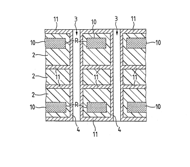
Figure 4 shows a first exemplary embodiment of the
structure or assembly of a multilayer constructed according
to the invention. Carbon-fiber resin prepregs 10 are
prepressed and subsequently further processed by drilling and
milling. Further processing consists in bringing in or
placing a drilling pattern or, more precisely, bringing in or
placing a layout related to the multilayer, which layout is
- 23 -
2 (~ 9 2
directly placed in the intermediate layer containing carbon
fibers. This layout can be, for example, a universal pattern
for gnd (the connecting path between the electric circuit and
the earth) or Vcc (the supply voltage terminal to a collector
circuit with respect to ground) or a very specific drilling
pattern. In any case, the layout is part of the total layout
such as, for example, a mask for fabricating a semiconductor
chip. This further processing of the intermediate layer can
be readily effected, for example, by means of computer aided
water-jet cutting, a technique which is fast and ensures
clean processing. The prefabricated layers or carbon-fiber
prepregs 10 are then laminated into the multilayer 1 such
that the carbon fibers cannot cause any electrical short
circuits, but are electrically conductive at locations where
conductivity is required. Entire conduc~or lines can be made
of carbon fibers, such conductor lines being embedded into
the multilayer like a scissor-cut and simultaneously bringing
about electrical conductance as well as mechanical
reinforcement.
If the carbon fiber Iayer has to be insulated, for
example, to an electrical throughbore or via 3, then "edges"
of the recesses or cut-outs in the carbon-fiber prepreg 10
are slightly rearwardly offset with respect to the actual
cut-outs of the drilling pattern in the multi-layer 1, as
depicted in Figure 4. In other words, the recesses or
- 2~ -
2~3~2
cutouts of the layout are always slightly larger as is the
case in the resin material of the multilayer.
However, as shown in Flgure 5, it is possible to
selectively utilize the electrical conductivity of the carbon
fibers. In this exemplary embodiment of the multilayer the
carbon fiber insert itself is laminated with an electrically
conducting material, preferably with copper. Such a
composite can be used as a current-conducting layer, for
example, as gnd or Vcc in a multilayer, next to layers or
prepregs as hereinbefore discussed in conjunction with the
embodiment illustrated in Figure 4. In such an application
the electrical conductivity of the carbon fibers naturally
has a positive effect. All current-carrying or live layers
are conveniently designated in Figure 5 by reference numeral
11, irrespective of whether this coincides with the
reinforcing carbon-fiber resin layers or not. In this
exemplary embodiment the mechanically stiffening,
electrically conducting layers are e~uivalent to or on a par
with the electrically conducting layers of the layout which
has no stabilizing effect. In certain regions or areas the
copper layer ll can be etched away in order to form an
electrical resistance- at the transition location
copper-carbon-copper, by means of which an electrical
component function is accomplished by the mechanically
stabilizing layers. This can be planned and included in the
pretreatment of the layout.
- 25 -
2 ~ 2
Another type of stabilization i9 depicted in Figure
6. In this assembly or structure the carbon fiber weave,
without resin, is galvanieally coppered prior to the
laminating operation, so that no copper/carbon fiber
laminates are used. In this manner, it is possible to
fabrieate highly stable and nevertheless ultra-thin
multilayers at a minimum of work and cost. ~he embedded
carbon fibers can likewise serve, as hereinbefore mentioned,
as eleetxieal conductor lines or also as resistanee elements
at locations where the additional eonducting layer is etched
away. Large parts or portions of the layout can thus be
transferred or applied to the carbon fibers, whereby
particularly thin, but nevertheless high-capacity multilayers
can be fabricated, which multilayers have mechanically
substantially improved in stability.
The carbon-fiber resin prepregs laminated with
copper with or without layout pre*reatment, but partieularly
the galvanized carbon fibers, with or without etched-away
eopper plating, ean be eonsidered to be semi- or
half-finished products serving for fabricating multilayer
printed wiring boards.
Figure 7 sehematically shows the appearance of
carbon fiber resin layers 11 subsequent to layout-related
pretreatment. Not particularly shown are the intermediate
layers, i.e. the etched planes or surfaees with the wiring
.
- 26 -
2 ~ 2
board layers. On the other hand, the planes consisting of
base material are indicated in broken lines, such base
material being glass fiber reinforced resin or the like.
Likewise not particularly shown in Figure 7 are the elements
of the insert technique according to Figure 6, i.e. the
current conducting carbon fiber bundles which can be provided
in a multilayer as mechanically reinforcing means and at the
same time as elements participating in the circuitry at
locations within the assembly or structure where they are
required in accordance with the layout. The asymmetrical or,
in other words, random arrangement of the carbon fiber
bundles improves the stabilizing effect without having the
hereinbefore mentioned disadvantage of the bimetallic effect
and a bending of the wiring board.
The use of carbon-fiber reinforced composite
materials for the fabrication of multilayers in multilayer
printed wiring boards for surface-mounted applications
provides, among others, the following advantages: good
mechanical machinability of the composite materials, a very
high modulus of elasticity and very low coefficient of the
thermal expansion of thé carbon fibers, low weight and, last
but not least, substantially more economical solutions in
comparison with the use of copper-Invar-copper laminates,
molybdenum or molybdenum/copper laminates.