Note: Descriptions are shown in the official language in which they were submitted.
2014901
"Protection device against the breakdown of bipolar transistors
in an integrated driving circu;t for power device with resonant
load on the coLLector"~
* * * * *
D E S C R I P T I 0 N
The present invention reLates to a protection device
against the breakdown of bipolar transistors in an integrated
driving circuit for power device with resonant Load on the
coLlector.
As is known, the maximum voLtage which may b- applied
across an integrated circuit is Limited by the breakdown
voltage of the bipolar transistors, both NPN and PNP, contained
in itA
It is also known that, for the breakdown voltage of a
transistor to be as high as possibLe, higher than the so-calLed
open base voltage, it 1s nocessary ~o mainta1n the base/emitter
voltage of the transistor itself at as Lo~ a value as possible,
in any case beLow that of the transistor's firing threshoLd.
In the specific case of driving stages for power devicec
the problem has already been partiaLly solved by short
circuiting to ground the base of the driving transistor~s) ~hen
the voltage applied across the integrated circuit is higher
than the open base breakdown voltase of the transistor(s)
themselves. In this way, due to a known effect, the breakdown
voltage of the affected transistor auto~aticaLLy rises above
2()~4901.
the open base vaLue.
This soLut;on, ho~ever, is onLy valid under normal
operating condi~ions, that is ~ith a collector voLtage of the
power device greater than zero.
In po~er devices ~ith resonant load on the colLector it
happens, however, that the parasitic capacitances and
inductances outside ~he integrated circuit periodically cause
the drop of the collector voltage belo~ zero. At that moment
the protection given by short circuittng the base of the
driving transistor(s) ;s no longer suff;c;ent, because the
base/emitter voLtage of the driving transistor is certainly
positive and tends to become higher than the firing tbreshoLd
of the transistor itseLf, ~hich consequently breaks do~n as
soon as the voLtage bet~een its coLlector and its ~aitter ;s
higher than the open base value.
The object of the present invention is to ovorcome the
limit of the kno~n technique described above, guaranteeing that
the voltage bet~een base and em;tter of any transistor of the
1ntegrated driving circuit may re~ain belo~ its firlng
ZO threshold even ~hen the collector voltsge of the po~-r dev;ce
be~4~e 5 negat1ve.
According to the invention such object is at~ained ~ith a
protect;on device characterized in that it co~prises auto~atic
com~utating means interposed between the base of the transistor
to be protected and the collector of the po~er device to cause
~(~14901
a flo~ of current having a lo~ voLtage drop bet~een said base
and said coLLector ~hen the collector voLtage faLls beLo~ a
predetermined vaLue.
In this way the drop of the coLlector voLtage beLo~ a
~inimu~ value, in particuLar beLo~ the vaLue of zero,
automaticaLLy determines, thanks to the conduction of ~aid
commutating means, the drop of the base/enitter voltage of the
transistor to be protected to a vaLuc ~hich is certainly beLo~
the firing threshold of the transistor itself ~ith consequent
raising of the breakdo~n voltage beyond the normaL open brse
value. The naximum voLtagc appLied across the integrated
circuit may thus increase without any problems, consequently
~idening the operating voLtage interval of the po~er device.
The construction and functional charactertstics of the
present invention shall be made more evident by the follo~ing
detailed description ot some of its embodiments tLLustrated as
non-limiting exampLes in the enclosed dra~ings, ~herein:
Fig. 1 sho~s the circu1t diagra~ of a driving stage for a
power device provided ~ith a protection device according to the
invention;
Fig. 2 sho~s the circuit diagram of a f~rst e~bodi~ent of
the protection device according to the invention;
Fig.s 3 and 4 sho~ possibLe forms of integration ot the
protection device of Fig. 2;
Fig. S sho~s the circuit diagram of a second embodi~ent of
20149C)~L
-- 5 --
She protect;on device according to the invention; Fig.s 6,
7 and 8 show posstbLe forns of integration of the protection
device of ~ig. 5.
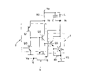
There is indicated in Fig. 1 ~ith 1 a Darlington-type
po~er device, for~ed by t~o NPN ~ransistors Q3 and Q4 having a
common colLector, the emitter of Q3 connected to thc base of Q4
and the emitter of a4 connected to thc base of the same Q4
through a resistance R1 and to ground through a resistance RS.
The common collector of the two transistors Q3 and Q4 is
connected to a voltage po~er supply Va through a rosonant Load
formed by a capacitance C and by an inductance L in paralleL
with one another~
To the pouer device 1 there is associatod a driving stage
2 comprising t~o bipolar NPN transistors Q0 and Q2 and a PNP
transistor Q1. The transistor Q2 has the emitter connected to
the base of transistor Q3 of the power device and th~ colLector
is connected to the power suppLy Va throu~h 8 resistance R2
external to the integrated circuit, the transistor Q1 has the
emitter and the coLlector connected to the colLector and to tho
base, respectively, of Q2, while the trsnsistor Q0 has the
collector and the e~itter connected to the base of Q2 and to
ground, respectively.
In conformity with the invention there is further provided
a protection device 3 a~ainst breakdo~n, ~hich in the examp~e
considered is shown appLied to the transistor Q2 onLy but may
201490~
in general be considered usabLe for any transistor of the
driving stage. The pootection device 3 has a ter~inaL 4
connected to the base of the transistor to be protected, in
this case Q2, and a terminaL 5 connected to the coLLector of
the po~er device, there being aLso provided a poLarization
terminaL 6 ~hich may be connected to any desired poLarization
voltage Vb, generaLLy positive but possibly even zero.
The protection device 3 is essentiaLLy a normaLLy
interdicted commutatlng means, ~hich is in a position of
commutating in Lo~ resistance conduction ~hen the coLLector
voLtage of the po~er device 1 faLLs beLo~ a pre-estabLished
value. In particular, ~hen the above coLLector voLtage,
indicated with Vc in Fig. 1, becc-~s negative, there is
estabLished through said commutating means, from the base of
transistor Q2 to the collector of the po~er dev1ce 1, a f~o~ of
current having a lo~ voltage drop ~hich ~flintains tho
base/emitter voLtage of Q2 at a Lo~ vaLue and ln any c~se not
higher than the conduct1On threshoLd of the sa~e transistor.
ConseqeuentLy the breakdo~n voLtage of the protected transi~tor
(in this case Q2) rises above the open base vaLue, thus
aLLo~ing the appLication across the integrated circuit
constituted by the po~er device 1, by the driving stage 2 and
by the protection device 3 a voLtage, ~ndicated ~ith Vs in Fi~.
1, having a vaLue higher than ~ouLd other~ise be allo~ed by the
open base breakdo~n voltage.
Z0~4901
A possible embodiment of the protection device 3 is
illustrated in Fi~. 2 and ccmprises an SCR configuration for~ed
by t~o bipo~ar transistors apl and QP2 of the PNP and NPN
types, respectively, the first of ~hich has the emitter
connected to the base of the protected transistor t1n this case
Q2), the base connected to the same emitter through a
resistance R3 and the collector connected to the poLar~zat1On
terminal 6 through a polarization resistance R4, ~hile tbe
second has the base connected to the base of thc same QP1 and
the emitter connected to terminal 5.
In operation, ~hile under normal cond1tions QP1 and qP2
are s~itched off, the drop of the colLector volta~e Vc to a
negative value causes the conduction of the two above nentioned
transistors and thus the desired flou of current from ter~ina~
4 to terminal S, that is, fro~ thè base of q2 to the collector
of the power device.
More precisely, ~hen voltage Vc bec~r~ negative, tho
base/emitter voltage Vbe of trsns~stor Q2 re~ains locked at the
value of the collector/emitter voLtage Vce of transistor QP1,
which at that point is strongly saturated (since the SCR is
switched on) and thus has a very small Vce (a few tens of
millivolts) which may here be called Vcesat tQP1).
The fol~ouing e~uations connect the voltaaes across the
different circ~;t branch points of Fig. 2:
Ve(Q2) = VbctQ3) ~ Vc
.
~~~90~
Vb(Q2) = - VcesatlQP1) + VbetQP2) ~ Vc
~hence:
Vbe(Q2) - Vb(Q2) - Ve(Q2)
= - Vcesat~QP1) + Vbe~QP2) - Vbc(Q3) t1)
But since transistor 4P2 is s~itched on and the
base/e~itter junction of Q3 is 1n direct operation, Vbe(QP2) is
approximately equal to vbc(a3) and equation (1) nay thus be
written:
Vbeta2) ~ Vcesattapl) in absoLute vaLue (2)
This result says that a2 operates ~ith a base/e~itter
voLtage of a fe~ tens of ~illivolts as long as the ~P1/~P2 SCR
is of a size such that Vcesat~QP1) is that desired, so that the
volta~e bet~een the col~ector and the e~itter of C2 ~ay bc
higher than the open base breakdo~n voltage of the sa~e
transistor.
The resistance R3, ~hich is not ~andatory, has th~ task of
preventing QP1 fro~ being s~itched on due to eddy current
effects, thus causing thc multiplicstion of such currents
~coning fron the point to be protected) ~or ~ts gain.
It should be noted that the invention does not invalidate
the operation of the po~er device outside the interva~ wherein
the voltage across the coLlector of the device ttse~f bect-Es
negative, because, during the device's nor~al operation~ the
voltage Vc rises at least up to the saturation Vce of the po~er
device (at Least 1 volt), so that aP2 ~and thus the SCR as
Z014901
~ell) is s~;tched off; this, in fact, has its base at the
voLtage of the polarization ter~inal 6 of the protect10n device
and the emitter at 1 volt, so that its base/e~itter voltage is
;n any case belo~ the conduction threshold.
One possible form of integration of the protection device
of Fig.Z is ilLustrated in Fig. 3, ~here according to the
teachings of US Patent No. 4.641.171 in the name of the sa~e
Appl;cant a layer 11 of the N~ type, a layer 12 of the P type
and an epitax;al substrate or layer 13 of the N type define the
emitter, the base and the collector, respectively, of
transistor Q3 of the po~er device and, inside an ;nsulat10n
pocket 14 of the P type, a layer 15 of the N type, a Layer 16
of the P type and a layer 17 of the N type detine the protected
driving Sransistor Q2.
~ccording to such form of integration the t~o protection
transistors GP1 and QP2 are ~ccomplished by exploiting t~o of
the structure's ;nternal parasitic ~ nents, both located
inside the ;nsulat~on pocket 14 and suitably connected tog~ther
as sho~n in Fig. 3. More precisely, the QP1 transistor of the
PNP type is accomplished by using as the emitter a layer 18 of
the P type, as the base a layer 19 of the N type and as the
collector a layer 20 of the P type physically connected to the
insulation pocket 14. The transistor aP2 of the NPN type in
turn has the collector in com~on ~ith the base of QPl and the
base in common ~;th the collector of apl ~connection to SC~)
2Q149~
- 10-
and 1ts emitter is connected to the coLLector of trans;stor Q3
of the po~er device, ~hat is, ~ith the epitaxiaL substrate or
Layer 13~ The poLarization resistance R4 is the Layer
resistance of the insulatlon pocket 14 and depends on ~he
geonetry ~ith ~hich the pa;r QP1/QP2 is designed and in any
case is of the order of several kohms. The terminaL 4 of the
protection device 3, corresponding to the emitter of OP1, is
connected to the base of Q2 ttransistor to be protected). The
ter~;naL 5, correspond1ng to the emitter of QP2, ls con~ccted
to the coLLector of Q3 tpower devlce). The terminaL 6 is
connected to the insulation pocket 14 and thus to ground in the
exampLe cons1dered in Fig~ 3. If the point to be protected
then has a high impedanc0, so that it couLd occur thst QP1 is
s~itched on due to eddy currents, lt ;s possible to insert the
reslstance R3 of F;g. 2.
As an alternative, the SCR device QP1/QP2 couLd be
accompLlshed as in Fig. 4, that is lnside a separate 1nsuLat1On
pocket 21. In such case it is possible to poLarize terminaL 6
of the protection device 3 at a voltage other than ground, and
in part;cuLar at a voltage h;gher than zero voLts and Lo~er
than the conduction threshold of Q2 if the sca iS to be
s~itched on ~ore eas;ly; if th1s voLtage is var;ed to~ards
Lo~er vaLues (even negative ones~, the 1gn;tlon of the SCR is
made more difficuLt.
Another possibLe embod1ment of the protect;on device is
2014901.
iLlustrated in Fig. 5 and comprises a single bipolar NPN
transistor QP3 having the collector connected to the base of
Q2, the emitter connected to the collector of Q3 and the base
connccted to the poLarization terminal 6 through the
polarization resistance R4.
The method of operation is similar to the preceding one,
that is the transistor aP3 is suitched on and thus deter~i~es a
flou of current having a Lou voltage drop from the base of Q2
to the coLLector of Q3 as soon as the latter's coLlector
voltage drops belou a predeternined value, and in particular
becones negative.
The base~emitter voltage of Q2 in this case is:
VbetQ2) = Vcesat(aP3) - VbctQ3)
so that u;th respect to the prevlous case there is the
advantage of a greater safety margin since, uith respect to
equation ~1), there no longer ;s the positive value of
Vbe(QP2), uhich contributed in keeping Vbe(a2) ~ore positive.
In addition, transistor aP3 may be designed so as to have
a louer collector series resistance, because it is possible to
use as the collector a larger area of the integrated circuit,
as shaLL appear evident later.
On the other hand, the flou of current between ter~inals 4
and 5 of the protection dev;ce is limited by the gain of QP3,
since there is no longer an SCR structure, so that the volta~e
drop betueen the tuo ter~inals is higher than that of the
Z01~90~
- 12 -
previous case.
The protection device of Fig. 5 may also be integrated in
compLiance ~th the rules established by the above mentioned US
patent. The protection transistor QP3 may then be formed by a
parasite transistor defined inside the sa~e insuLation pocket
14 of the driving transistor a2 (Fig. 6) or inside a separate
insulation pocket 21 ~Fig. 7).
A further method for accompL~shing transistor aP3 is that
illustrated in Fig. 8, ~herein the same base and e~itter
diffusions are used (layers 12 and 11 of Fig.s 3 and 4) of
po~er transistor Q3. There is then a change in the vaLue of
polarization resistance R4, ~hich is that of layer 12 of Fig.s
3 and 4 and ~hich is only of some hundreds of ohms~
It should lastly be noted that the present inv-ntion,
described ~or a monolithic assembly, may also be accompLished
~ith the po~er devlce and the drivin3 stage ~ith the
corresponding protection device on t~o separate plates. ln
such a case it is necossary to accomplish on a specia~ p~ate
the c~m~nents of the protection circuit according to the
structures seen above (extract;ng them from Fig.s 3, 4, 6, 7
and 8) and then to make the connections sho~n in Fig.s 2 and 5.
.